Design and Prototype of an Automated System for
Commercially Viable Production Using
Micro Contact Printing
by
Karan Chauhan
M.Eng in Manufacturing
Massachusetts Institute of Technology, 2006
Submitted to the Department of Mechanical Engineering in Partial
Fulfillment of the Requirements for the Degree of
Master of Engineering in Manufacturing
at the
Massachusetts Institute of Technology
August 18, 2006
Copyright 2006 Massachusetts Institute of Technology. All rights reserved
Signature of the A uthor ...
Department of Mechanical Engineering
August 15, 2006
C ertified by ...
A Cil b
David E. Hardt
Professor, Mechanical Engineering
Thesis Supervisor
... ...
Lallit Anand
Chairman, Departmental Committee on Graduate Studies
Department of Mechanical Engineering
MASSACHUSMtTS INSTMtE OF TECHNOLOGY
JAN 2 3 2007
BARKER
Design and Prototype of an Automated System for Commercially Viable
Production Using
Micro Contact Printing
by
Karan Chauhan
Submitted to the Department of Mechanical Engineering on August
1 6 h,2006 in Partial Fulfillment of the Requirements for the Degree of
Master of Engineering in Manufacturing
Abstract
This dissertation is a documentation of the thought process, its justification and the implementation details that went into prototyping a fully automated system employing Micro Contact Printing, an emerging technique for replication and pattern
transfer using soft organic materials, for a nano technology based company in Cambridge, Massachusetts during the summer of 2006. The thesis takes the reader
through an extensive literature review of the suite of soft lithography techniques
-Near Field Soft Optical Lithography, Replica Molding and Micro contact printing
-focused on the critical factors for taking these techniques from research facilities to commercial manufacturing facilities. Micro Contact Printing was studied more
extensively than the others. We propose a system level design for viable manufacturing using micro contact printing and also present the implementation
Acknowledgements
I would like to dedicate this thesis to my teammates in this project - Hyung Jun Kim & Arthur Cao Yuan (my colleagues in the M.Eng program), Prof David Hardt (Professor, MIT) and Brian Mayers (Senior Scientist, Nano-Terra, LLC). I think we coordinated closely as friends to finish an ambitious project within the limited time.
Prof Hardt was with us whenever we needed advise and also took a most important role of monitoring our progress. The long and rather informal weekly meetings with him always provided us with new ideas as well as deepened our commitment to the success of this project and insight into the discipline of manufacturing. I take this opportunity to congratulate him for this new degree program at MIT and sincerely wish the future batches my best.
I also thank Brian and the rest of the Nano-Terra team for providing a very friendly and supportive atmosphere at Nano-Terra. I appreciate the enormous amount of trust they showed in us and our decisions throughout the project. Without Brian acting as the crucial link between science and engineering, it could have been hard to realize our project goals.
Table of Contents
A b stra ct ... 1
Acknowledgements ... 2
List of Figures ... 6
Chapter 1 Introduction and Soft Lithography ... 9
1.1 An Introduction to Soft Lithography ... 9
1.2 The Soft Lithography Taxonomy ... 10
1.3 Soft Lithography versus photolithography ... 15
1.4 Overview of the Thesis ... 16
1.5 Conclusions 17 Chapter 2 18 Near Field, Phase-Shifting, Soft Optical Lithography ... 2.1 Introduction ... 18
2.2 Physical principles of the process ... 19
2.3 A Process Modeling Framework for NFPSOL ... 22
2.3.1 The input and output parameters of interest ... 22
2.3.2 Sources of disturbance and variation ... 24
2.3.3 Attempts on Process Modeling ... 25
2.4 The Steps Involved in the Process ... 26
2.5 Comparison with Current Lithography Practices ... 27
2.5.1 Advantage ... 27
2.5.2 Currently Unsolved Issues and Challenges ... 28
2.6 Conclusions 29
M icro contact P rinting ... 30
3.1 Introduction ... 30
3.2 Principles and characteristics of Micro contact Printing ... 30
3.2.1 Formation of Self Assembled Monolayers or SAMs ... 31
3.3 Micro contact printing Procedure ... 33
3.4 Critical Factors for pCP ... 34
3.5 Summary of manufacturing considerations ... 41
3.6 Industrial design efforts for Micro contact printing ... 43
3.7 C onclusions ... 44
Chapter 4 Concept Design and Realization ... 45
4.1 Introduction ... 45
4.2 The Inking Process ... 46
4.2.1 Designs for Inking ... 47
4.3 The Stamping Process ... 50
4.3.1 Designs for Stamping ... 51
4.4 A Manufacturing System for High Volume Production ... 61
4.5 C onclusions ... 63
Chapter 5 Automation Hardware and Software ... 64
5.1 Introduction ... 64
5.2 The Automation Approach ... 64
5.3 The Mechanical Elements for Automation ... 65
5.3.1 The XY-Manipulators...66
5.3.2 The Rotary Positioning Table ... 68
5.3.3 The 2 Lead Screws for Inking and Lifting ... 68
5.4 The Electronic and Software Elements for Automation ... 69
5.4.1 The Motors and Motor Drivers ... 69
5.4.2 Motor Driver-Controller Interface ... 74
5.4.3 NI-Motion Architecture ... 74
5.4.3.1 NI Motion Controller Architecture ... 76
5.4.3.2 NI Motion Controller Functional Architecture ... 75
5.5 Kinematic Analysis of the Motion ... 78
5.6 Execution of the Application ... 96
5.7 C onclusions ... 96
Chapter 6 6.1 Conclusions and Future Work ... 97
L ist of R eferences ... 99
List of Figures
Figure 1.2.1: Schematic illustration of the procedure for fabricating PDMS stamps 10 from a master having relief structures on its surface.
Figure 1.2.2: Schematic procedures for pCP of hexadecanethiol (HDT) on the surface 11 of gold: (a) printing on a planar surface with a planar stamp.
Figure 1.2.3: Schematic procedures for replica molding. 12
Figure 1.2.4: Schematic procedures for MIMIC. 12
Figure 1.2.5: Schematic procedures for pTM 13
Figure 1.2.6: Schematic procedures for SAMIM. 14
Figure 2.1: Some applications of NFPSOL. 19
Figure 2.2: The concept of Phase Shifting Optical Lithography to increase resolution. 20
Figure 2.2.2: The optical phenomenon behind NFPSOL. 20
Figure 2.3.1: A typical feature developed with NFPSOL. 22
Figure 2.3.1: Variation of the output (Line width) with phase shifter depth, wavelength 23 content and edge spacing on the relief face of the mask.
Figure 2.3.3: Scalar diffraction theory. 24
Figure 2.3.4: Full Vector Finite Element Method. 24
Figure 2.4: The Process Steps involved in NFPSOL. 26
Figure 3.2.1: Schematic illustration depicting the application of a PDMS stamp 30 containing thiols to a polycrystalline metal film.
Figure 3.2.1. Self assembled monolayers. 31
Figure3.4.1: Relationship between thicknesses printed with 0.2 milli Mole solution of 34 ECT ink.
Figure 3.4.2: Relationship between printing time and the number of defects in the 34 pattern.
Figure 3.4.3: Quality of Micro contact printed gold structures performed in the case of 35
an ECT contact-inked stamp.
Figure 3.4.4: Illustrations of (a) basic geometry of a PDMS stamp and stamps 36 deformed into contact with substrates under (b) required minimum and (c) excess
pressures.
Figure 3.4.5.1: Three different types of inking for Micro contact printing. 37
Figure 3.4.5.2: Three contact propagation methods. 38
Figure 3.4.5.3: Schematic illustration of possible deformations of microstructures in 40 the surfaces of elastomers
Figure 3.6.1: Schematic procedure for conducting iCP with a rolling PDMS stamp. 41
Figure 3.6.2: A vertical Cross-section of the wave printing prototype. 42
Figure 4.2.1.2: The basic concept of polygonal inking. 47
Figure 4.2.1.3: The finalized inking design. 48
Figure 4.3.1.1.A Roll Stamping. 50
Figure 4.3.1.1.B Elastic strain induced in the stamp with Roll Stamping. 51
Figure 4.3.1.2.A: The basic concept of polygonal stamping. 52 Figure 4.3.1.2.B: The stamping tool proposed for Polygonal Stamping. 52 Figure 4.3.1.2.C: The hinge effect of the polygonal stamping tool. 53
Figure 4.3.1.3: An illustration of the steps in Pseudo Roll Stamping. 54
Figure 4.3.1.4: Two foam covered cylindrical wipers apply the gold coated PEN sheet 58 onto the PDMS stamp.
Figure 4.3.1.5: A step by step illustration of the stamping design developed. 58
showing the integration between the inking-stamping steps and etching.
Figure 4.4.2: Another version of the manufacturing system discussed before.
Figure 5.4: A device level schematic of the hardware-software integration for automation.
Figure 5.4.1: Speed-torque characteristics for the Motor.
Figure 5.4.2: The basics of a stepper motor system.
Figure 5.4.2: The layout of the acquired driver MD2S-P.
Figure 5.4.3: NI Motion Control Hardware and Software Interaction.
Figure 5.4.3.1: Physical NI Motion Controller Architecture.
Figure 5.4.3.2: Typical NI 73xx Motion Controller Functional Architecture.
Figure 5.5.A: A simplified illustration of the elements involved in the stamping step.
Figure 5.5.B: Kinematic analysis for Move 1.
Figure 5.5.1.1: Figure 5.5.1.2: Figure 5.5.2.2: Figure 5.5.2.2: Figure 5.5.3.1: Figure 5.5.3.2: Figure 5.5.4.1: Figure 5.5.4.2: Figure 5.5.5.1: Figure 5.5.5.2:
The calculated angular speed of the supply spool vs time.
The computed and used electronic gear ratios.
The calculated angular speed vs time for the SUPPLY axis for Move 2.
The computed and used electronic gear ratios.
The calculated angular speed of the DRIVE axis vc time for Move 4.
The computed and used electronic gear ratios.
The calculated angular speed vs time for the DRIVE axis for Move 6.
The computed and used electronic gear ratios.
The calculated angular speed vs time for the DRIVE axis for Move 8.
The computed and used electronic gear ratios.
62 68 70 71 72 74 75 77 79 80 81 82 84 84 87 88 90 91 93 94
Chapter
1
Introduction and Soft Lithography
1.1 An Introduction to Soft Lithography
Soft Lithography comprises a set of techniques that uses soft materials to enable replication and pattern transfer on a wide range of dimensional scales, ranging from nanometers to centimeters. These techniques follow a non-photolithographic strategy for pattern transfer based on self-assembly' of molecular layers and replica molding for carrying out micro and nanofabrication.
Most Soft Lithography techniques have been recently developed and have attracted significant attention from both academia and industry due their tremendous potential to support or even replace conventional means of micro manufacturing. The low capital costs and potential for high volume manufacturing with a variety of materials are significant attractions as well. The control over surface chemistry, required for some applications in medicine, is possible if using soft lithography. Other potential applications of soft lithography in the near future could include simple optical devices such as polarizers, filters, wire grids, and surface acoustic wave (SAW) devices [1]. Longer term goals include working toward optical data storage systems, flat panel displays, and quantum devices [2].
Self-assembly is the spontaneous aggregation and organization of subunits (molecules or meso-scale objects) into a stable, well defined structure via non covalent interactions. The information that guides the assembly is coded in the properties (e.g. topologies, shapes, and surface functionalities) of the subunits; the individual subunits will reach the final structure simply by equilibrating to the lowest energy form. Because the final self assembled structures are close to or at thermodynamic equilibrium, they tend to form
1.2 The Soft Lithography Taxonomy
Several different techniques are known collectively as soft lithography. Holistically, every soft lithography technique formally consists of three steps:
(1) Fabrication of a topographically patterned master, for example on a silicon wafer, using a conventional process like photolithography.
(2) Molding this master with a functional organic material (usually Polydimethyl siloxane or PDMS) to generate a patterned template.
(3) Generating a replica of the original template in a functional material or a 1:1 projection of the pattern on a surface by applying the stamp.
Fabrication and silanization of master SIO,,SiN4,metals.
photoresists or wax
Pouring of PDMS over master
PDMS
Curing, and releasing of PDMS
PDS d (1'4J.99b) Doformation of PDMS Pairing Sagging (h>>d) /d <dc~h)/
Figure 1.2.1: Schematic illustration of the procedure for fabricating PDMS stamps from a master having relief structures on its surface [3].
The techniques which are collectively known as Soft Lithography techniques are:
(A) Near Field Optical Lithography
A transparent PDMS mask with relief on its surface is placed in conformal contact with a layer of photo resist. Light, from a source, passing through the stamp is modulated in the near-field. If the relief on the surface of the stamp shifts the phase of light by an odd multiple of 7r, a null in the intensity is produced. Features with dimensions between 40 and 100 nm are produced in photo resist at each phase edge [4]. This process shall be discussed in detail in Chapter 2.
(B) Micro-contact Printing(pCP)
A thin layer composed of an alkanethiol and ethanol, called "ink" is spread on a patterned PDMS stamp. The stamp is then brought into conformal contact with the substrate, which can range from coinage metals to oxide layers. The thiol ink is transferred to the substrate where it forms a self-assembled monolayer, or SAM2, that can act as a resist against etching. Features on the substrate are revealed after etch treatment. Features as small as 300 nm have been produced in this way [5]. This process shall be discussed in detail in Chapter 3.
2 SAMs can be easily prepared by immersion of a substrate in the solution containing a ligand (Y(CH2)nX) reactive toward the surface, or by exposure of the substrate to the vapor of a reactive species.
A i
Print SAMs X
S I (CH2)"
si
Etch Dqposit
Figure 1.2.2: Schematic procedures for pCP of hexadecanethiol (HDT) on the surface of gold: (a) printing on a planar surface with a planar stamp [11].
(C) Replica Molding
A PDMS stamp is cast against a conventionally patterned master. Polyurethane is then molded against the secondary PDMS master. In this way, multiple copies can be made without damaging the original master. The technique can replicate features as small as 30 nm [6].
>50 rim
Mold prepolymer
Cur. pe off
Figure 1.2.3: Schematic procedures for replica molding [4].
Continuous channels are formed when a PDMS stamp is brought into conformal
contact with a solid substrate. Capillary action fills the channels with a polymer
precursor. The polymer is cured and the stamp is removed. MIMIC is able to generate
features down to 1 pm in size [7].
PDMS mold support Place a drop of prepolymet at one end Fill channels by capillary action
Cure, remove mold
Figure 1.2.4: Schematic procedures for MIMIC [4].
(E) Micro transfer Molding (uTM)
A PDMS stamp is filled with a prepolymer or ceramic precursor and placed on a
substrate. The material is cured and the stamp is removed. The technique generates
features as small as 250 nm and is able to generate multilayer systems [8].
prepolymer
Remove excess prepolymer
Place on the suppon
Cure, romove mold
residual film
Figure 1.2.5: Schematic procedures for p TM [4].
(F)
Solvent-assisted Micro contact Molding (SAMIM).
A small amount of solvent is spread on a patterned PDMS stamp and the stamp is
placed on a polymer, such as photo resist. The solvent swells the polymer and causes it to expand to fill the surface relief of the stamp. Features as small as 60 nm have been produced [9].
PDMS mold
wetting
liuid Place the mold on a support
po mor film Support Evaporate solvent Remove mold support - residual film
Figure 1.2.6: Schematic procedures for SAMIM [4].
1.3 Soft Lithography versus photolithography
Soft Lithography techniques not only promise a significantly cheaper alternative to the currently employed photolithography techniques, but also allow for more flexibility in product choices (for example, manufacturing structures on a non-planar surface, controlling chemistries of a surface etc), resolutions and feature sizes.
Comparison between photolithography and soft lithography
Photolithography Soft lithography
Definition of patterns Rigid photomask Elastomeric stamp or mold
(patterned Cr supported (a PDMS block patterned
on a quartz platelf with relief feantres) Materials that can be Photoresists Photoresistsae
patterned directly (polymers with
photo-sensitive additives)
SAMs on Au and SiO, SAMs on Au. Ag. Cu. GaAs. Al. Pd. and SiOGa
Unsensitized polymnersb (epoxy. PU. PMMA. ABS.
CA. PS. PE. PVC) Precursor polymerscd
(to carbons and ceramics)
Polymer beadsd Conducting polymersd Colloidal inaterialsad Sol-gel materials-d
Organic and inorganic saltsd
Biological macromolecules" Surfaces and structures Planar surfaces Both planar and nonplanar
that can be patterned 2-D structures Both 2-D and 3-D structures Current linits to -250 nui (projection) -30 nnih"'. -60 nie. ~I pmde
resolution -- 100 nin (laboratory) (laboratory)
Minimuml feature size -100 n (?) 10 (?) - 100 im
"Malde by (a,) ICP. (b) REM. (c pTM. () MIMIC. (e) SAMIM. PU:polyurethane: PMMA: poly(mielhyl inethacrylatei. ABS: polyt acryloiutnle-buitadiene-styrene): CA: cellulose acetate. PS: polystyrene: PE. polyethylene: and PVC: polyminyl chloride t
Table 1.3: A tabular comparison between Soft Lithography and conventional optical lithography [10].
1.4 Overview of the Thesis
This thesis is a documentation of the thought process, its justification and the implementation details that went into prototyping an automated micro contact printing system for a nano technology based company in Cambridge MA during the summer of 2006. The objectives of this project were:
1. To understand and evaluate the capability for high volume production using soft lithography techniques based on the current state of knowledge about the
processes and ongoing industrial and laboratory efforts. The techniques studied were near field soft optical lithography, replica molding and micro contact printing.
2. To conceptualize a manufacturing system built upon micro contact printing, to achieve economically viable production.
3. Based on a feasible manufacturing system design, implement a prototype that demonstrates automated inking, stamping and the tool/substrate transfer for micro contact printing.
Chapter 2 describes Near Field Phase Shifting Soft Optical Lithography- a soft lithography process- that was studied for feasible manufacturing. Chapter 3 describes the principles of micro contact printing, the current state of the art and critical factors for manufacturing including some feasible designs. Chapter 4 describes the overall design of the prototype that was developed. Chapter 5 provides details about the hardware and software integration to achieve automation in the prototype. Chapter 6 concludes this thesis with scope for future work. The C/C++ source code for the software application and references can be found in the appendices.
1.5 Conclusions
The chapter introduced the reader to the scope and objectives of this project. A brief overview of the various soft lithography techniques was also presented. The next chapter will discuss one of the soft lithography techniques called Near Field Soft Optical
Chapter 2
Near Field, Phase-Shifting, Soft Optical Lithography
2.1 Introduction
This chapter discusses Near Field Optical Lithography - an innovative optical lithography technique, which falls within the realms of soft lithography. The technology uses patterned elastomeric PDMS masks in conformal contact with a layer of photo resist to selectively expose (through the pattern on the mask) the photo resist to light and cure it before conventional chemical etching to generate edged patterns. In a laboratory setup, this approach requires only a phase mask and a handheld UV lamp to generate structures with dimensions as small as 50 nm over large areas (many cm2, limited only by the size of the mask)[12]. The technique has been applied to make nano wires, micro rings and arbitrary shapes as shown in figure 2.1.
To distinguish from other forms of optical lithography (which also use phase shifters) we shall refer to this process henceforth as "Near Field, Phase Shifting, Soft optical Lithography" or as NFPSOL in the abbreviated form.
Nano Wires
urn[f I - 1 PM fnu
Arbitrary shapes Micro Rings
Figure 2.1: Some applications of NFPSOL [13].
First, this chapter discusses the physical principles, the process steps involved to
produce parts, the current state of development of this technology and possible
applications. Then, the technology is critically compared on various parameters to the
commercially established technologies for optical lithography. The chapter concludes
with an analysis on the feasibility of high volume production using this technique along
with some system and process level concept proposals.
2.2 Physical principles of the process
Optical lithography exploits the behavior of certain photosensitive polymers (called
photo-resists) when exposed to light. Some photosensitive polymers, by the nature of
their chemical composition, may absorb the light and harden" (or cure) while others may
disintegrate. A layer of such a polymer is uniformly applied onto a substrate, selectively
exposed to light through an optical system including a lens and a mask and the uncured
polymer is removed. Then, during the chemical etching of the substrate, the cured
polymer protects the covered portions of the substrate to result in an image of the pattern
on the substrate.
There exist several ways in which patterns on a mask could be transferred onto the
photo resist and then the substrate. The conventional forms of lithography use a hard
mask with a chrome coat to block incident light selectively onto' a layer of photo resist
and then develop the photo resist.
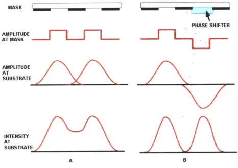
The use of relief features on masks is not new. Phase-shifting optical lithography with hard masks in the far field has been commercially employed to achieve very high resolutions [14]. The intensity of the light at the substrate can be modulated by appropriately inserting optical media and thereby changing the optical path length and the phase difference. Figure 2.2 explains the concept of phase shifting lithography.
MASK AMPLITUDE AT MASK AMPLITUDE AT SUBSTRATE INTENSITY AT SUBSTRATE A PHASE SHIFTER B
Figure 2.2: The concept of Phase Shifting Optical Lithography to increase resolution. (A) Without using phase shifting media in the optical path. (B) Inserting a phase shifting media to
alter the phase difference at the substrate and hence the intensity distribution.
Soft lithography uses relief and recess features, patterned on a transparent and elastomeric PDMS photo mask. NFPSOL achieves selective blocking of light in the near field through relief features in the mask so that the each step on the relief surface of the mask translates to constructive or deconstructive interference of light on the photo resist
surface, depending on the relief height used. A relief height of odd multiples of (/2)
gives destructive interference at the relief edge which that of multiples of X give constructive interference.
uv light
phase mask
resist
develp I
100 nm
Figure 2.2.2: NFPSOL- Formation of features [24].
LIGHT
0TJLK
.4 -2 0 2 4 -4 -2 0 2 4 Distance (JAm) PDMS MASK INTENSITY PROFILE ON THE SUBSTRATE RESULTING SURFACE OF TESUBSTRATE (Negate photoressAFigure 2.2.2: The optical phenomenon behind Near Field, Phase Shifting, Soft Optical Lithography [15].
The elasticity of the mask material, PDMS, and its near perfect conformance with a
mating surface, give soft optical lithography some significant advantages over
conventional optical lithography despite some limitations.- We shall discuss them in
section 2.4.
2.3 A Process Modeling Framework for NFPSOL
Causal modeling of any process provides a framework for identifying the critical parameters that affect output quality from a manufacturing process. The unavailability of relevant data from experiments or academia will restrict this section to identification of the input and output parameters of interest and also the sources of disturbance cause variance in the process output.
2.3.1 The input and output parameters of interest
The three most important input parameters which would determine the output and its
quality are listed as below:
1. The incident light
-The intensity of the incident light -The exposure time
-The wavelength content
2. The PDMS mask
-Density of relief features on the mask
-Height of the relief features or the phase shifter depth.
-Transmission coefficient of PDMS.
3. The photo resist and development parameters.
-Behavior to light exposure (i.e, threshold intensity etc)
-Thickness of the photo resist layer.
-Post exposure bake (PEB) temperature and time. The process outputs of interest are:
1. Line Width and section profile of the lines on the photo resist which can be expressed
as an "unknown" function of incident light intensity, density of features on the mask and the wavelength content of the incident light as the prime factors.
Figure 2.3.1: A typical feature developed with NFPSOL. Line width is defined as the width of the feature at half the height from the bottom [13].
2. Resolution or the spacing between the lines on the photo resist which is related to the density of features on the mask and the incident light intensity.
LInfwidth vs. Shifter Depth 407 nm and 360 nm bandpass iter* 1000 800I-.38n em0 360 nrn 400 -.- 407 nrm 200 - -
1
440 44 460 455 480 465 Phase-shifter depth (nm)Lewidth , sphise-utles depth usui 36C tun and 407 :un bandpass filtei s , Exposur tim - s0
240 220 200. 180 160 120 0 10 20 30 40 50
Edge spehg on the i eNef lace of the mask tumP
Figure 2.3.1: Variation of the output (Line width) with phase shifter depth, wavelength content and edge spacing on the relief face of the mask [16].
2.3.2 Sources of disturbance and variation
There are some factors which could affect output quality in the process even if perfect
incident light and photo resist's exposure behavior is ensured. They are listed below.
1. The distortions in the PDMS photo mask while peel off from the master pattern, while
handling during the process and on cyclic exposure to light on absorption of radiation.
2. The contact between the PDMS mask and the photo resist surface could be
non-conformal due to possible trapping of air or particulate matter.
3. The post exposure treatment time of the photo resist has been known to have large
variation [17]
2.3.3 Attempts on Process Modeling
The observed results have deviated slightly from those predicted by optics theory.
Figure 2.3.3 shows that the resulting features on the photo resist layer are not as expected
by the scalar diffraction theory [18].
MASK PROFILE
INTENSITY PROFILE AS PREDICTED BY
Wider, Higher & 0 SCALAR DIFFRACTION THEORY
rougher .4 -2 0 2 4
ACTUAL FEATURES ON THE PHOTO RESIST LAYER
4 .2 0 2 4
Disiance (pim)
Figure 2.3.3: Scalar diffraction theory. The features formed corresponding to the relief features
of the mask are wider, rougher and have greater average height than those corresponding to the
recess features on the mask [11].
A better explanation of the process can be found with Full Vector Finite Element Methods [19]. Their method explains the anomalies in the scalar diffraction theory.
-4 .2 0 2 4 Distance
Figure 2.3.4: Full Vector Finite Element Method [11] provides a better explanation than
the scalar diffraction theory.
2.4 The Steps Involved in the Process
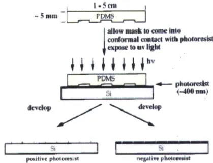
Manufacturing parts using NFPSOL begins with the fabrication of a "master pattern" on a silicon wafer using any of the conventional lithography techniques. The master pattern is used a mold and liquid PDMS is poured into it. The solid PDMS is peeled off to give a PDMS mask with the desired relief and recess features. This mask is placed in conformal contact with a layer of baked photo resist on a substrate and exposed to UV light. Post exposure development is followed by etching to get the desired pattern onto the substrate. Further refinements like oxidation to reduce feature size or metallization are product specific.
1. Acquisition of a defect free PDMS mask.
2. Setting the process parameters.
3. Spin coating photo resist (about 3000 RPM for about 60 Seconds).
4. Soft bake -100-135 OC (for about 60 to 90 Seconds on a preheated plate).
5. Conformably place the PDMS mask onto the photo resist layer.
6. Expose to light (between 1-15 Seconds). 7. Post exposure baking (for about 30 Seconds). 8. Develop the exposed resist (30 to 60 Seconds).
allow mIsk t coe
11tcoEoraal Onutact with pbotormt;
expowe to Ow light
*"loplo
S
poeiuve pholomut
Figure 2.4: The Process Steps involved in NFPSOL.
2.5 Comparison with Current Lithography Practices.
NFPSOL has several advantages in terms of capability over the current lithography practices due to the properties of the mask material -PDMS. The elasticity of PDMS and its ability to make a near perfect conformal contact with any arbitrary shape allows its use for patterning on non-planar surfaces- which only the expensive, and slow "Scanning near
field optical lithography", or SNOL, can accomplish [20]. The other great advantage is
the cost effectiveness of the process which does not use the expensive optical systems used in current commercial practices. Also, it is likely that the automation required might be cheaper than that for the convention means of optical lithography owing to the simplicity of the process. We shall first briefly discuss the key advantages and then move
to the issues and problems which prevent this technique from being applied commercially as of today.
2.5.1 Advantage
The advantages of Near Field, Phase Shifting, Soft Optical Lithography over conventional lithography techniques are listed below.
1. Capable of patterning features on planar as well as non-planar surfaces.
2. Capable of patterning large area (up to several sq meters). The area is limited only by the area of the PDMS mask used.
3. Low capital and running costs.
4. Parallel energy transfer and thus faster processing as compared to the step and scan optical lithography systems.
5. Feature size and resolution as low as 30nm has been demonstrated in laboratories
[21]
2.5.2 Currently Unsolved Issues and Challenges
Despite its capabilities and promise of low cost for high volume production, Near Field, Phase Shifting, Soft Optical Lithography has not been used commercially for production as of today. Some of the assignable causes for the same could be:
1. No single process model can accurately predict the output given a set of inputs. That is, the knowledge about the process physics is probably still under-developed. 2. Deformation of the PDMS masks while peeling off from the master, while
handling during the process (due to gravity as well as adhesion forced with the photo resist layer [22]) and on cyclic exposure to light- is detrimental to output quality.
3. Difficult to produce multi-layered patterns as the elastic nature of the mask makes registration very difficult. This limits its use for .only certain single layer
4. Obtaining multiple feature sizes and resolutions for the same product is not addressed.
2.6 Conclusions
In this chapter, we described a soft lithography technique which achieves pattern transfer by modulation of light in the near field using elastomeric masks with relief features on its surface. The process is still under development as academia works towards a better explanation of the phenomenon. The process promises great potential in the future and the major challenge involves achieving registration for multi layered applications. In the subsequent chapters, we will discuss micro contact printing in detail and our efforts towards taking this technique from the laboratory to industry.
Chapter 3
Micro contact Printing
3.1 Introduction
Micro contact Printing (or pCP), as it will be frequently referred to in this text) uses the relief patterns on a PDMS stamp to form patterns of self-assembled monolayers (SAMs) of inks on the surface of a substrate through conformal contact. Micro contact printing differs from other printing methods, like inkjet printing or 3-D printing, in the use of self-assembly (especially, the use of SAMs) to form micro patterns and microstructures of various materials [25].
This chapter provides a literature review of the process including its principles and characteristic features. We also discuss some industrial design efforts to take this technology from the laboratory to commercial production.
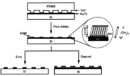
3.2 Principles and characteristics of Micro contact Printing
Micro contact printing is a method for patterning Self-Assembled Monolayers (SAMs) on surfaces using elastomeric stamp [26]. The most distinct characteristic of UCP is its use of self-assembly (especially, the use of SAMs) to form micro patterns on a substrate [27]. SAMs are formed by contact between a topographically patterned elastomeric stamp, wetted with an ink consisting of molecules that are capable of forming SAMs, and the surface of substrate.
Micron scale SAMs by Micro contact printing can be formed manually in a
conventional chemical laboratory and it does not require any photolithographic
equipment or a clean room environment. Therefore, the simplicity and economic
efficiency for patterning micron scale layer are major benefits of Micro contact printing.
Another Characteristic of MCP is conformability. Because the Micro contact printing
uses PDMS stamps, the stamp is able to conform to substrate with little external normal
force and at the same time can compensate for the surface roughness of the substrate.
This is important in transporting molecular level SAMs.
3.2.1 Formation of Self Assembled Monolayers or SAMs
Self-Assembled Monolayers (SAMs) are layers formed on a solid surface by
spontaneous organization of molecules. It has been reported that a polymer inked with
an alkanethiol and brought into contact with a gold-coated surface can form a monolayer
of these molecules in the areas of contact [29].
PDNIS
Vapor aDiffusion from Stamp
Transpot Surface
jDIffuson'
Metallic Grains;
---of Substrato SO nm
Figure 3.2.1: Schematic illustration depicting the application of a PDMS stamp containing
thiols to a polycrystalline metal film. The mechanisms of mass transport from the stamp to
The ink used in Micro contact printing to form the SAMs is mainly transported through diffusion at the stamp-substrate interface. Diffusion from the- edges of the stamp and vapor transport are the non-contact mechanisms that can also form SAMs (see figure
3.2.1). When the target feature sizes are smaller than 500 nm, these non-contact transport
mechanisms become significant enough to degrade the output quality [31].
The substrates, on which the SAMs are formed, are generally prepared by common physical vapor deposition (PVD) methods, i.e., thermal or electron beam evaporation. Among a wide range of materials used for substrates, gold is the most commonly used as it is easily available as a thin film and easy to pattern by a combination of lithographic tools (photolithography, micromachining) and chemical etchants. In addition, gold is a very inert material, so it does not oxidize at temperatures below its melting point. However, silver [13] and copper [14] have been used as a substrate for forming SAMs through Micro contact printing.
(A) Oran ' 'nterfce:
Determnine surtace poer ties Prewwtnt chemkiai fjn( teon.0 group! lermind
DIneOrganic Intrphos 1 3 av.
PrcwicWe welf-def,,nd lhckne-%
All OClhi~)Alt tt i. el".?(A itI l U ctU(ivity
t~~s Sta1oii7es5 surtace~ atoms
Suostrate M le P lc ttates
Dense,
(B) Wall-ordered Disordered Striped
Structure* Structures Phaaos
Figure 3.2.1. Self assembled monolayers. (A) Schematic diagram of an ideal, single-crystalline SAM of alkanethiolates supported on a gold surfaces (B) The variety of structural arrangements found in SAMs prepared by gCP when the stamp is wetted with a 1-10 mM solution and applied
3.3 Micro contact printing Procedure.
Micro contact Printing can be thought of as a two stage process: Inking and Stamping.
Inking consists of wetting with the ink and drying. Ink that forms SAMs is transferred
through a solvent such as ethanol, so solvent needs to be removed after transferring ink to
stamp. The wetting step is applying ink solution to a PDMS stamp and drying step is
removing solvent from PDMS. Solvent can be dried in the air, but a steam of nitrogen gas
helps to reduce time for drying. Inking and drying times depends on factors such as ink
concentration, printing area, and printing method. Typically, inking step takes 30 ~ 60
seconds and drying step require 10 ~ 60 seconds.
The stamping process comprises 3 sub-steps: Initial contact & propagation, full contact,
and separation. Achieving full contact through gradual contact is important in order to
minimize air trapping between stamp and substrate. After achieving full contact, contact
time is required to transport inks from a stamp to a substrate and form SAMs. The
required length of contact time can be different mainly according to ink type,
concentration of ink or target thickness of SAMs.
Abanmtol "ink"
4-Au I T1
Subftra
SPrtnlSAMu
Substra 1 X
(CH
2S
Table 3.3 summarizes the process, the required time and typical failure modes of Micro contact printing reported through the research so far.
Process Inking Stamping
Step Immersion Drying Initial contact and Self assembly full Peeling off
propagation contact
Time 30 - 60 sec 10 - 60 sec I - 5 sec 0.3 - 60 sec l-5 sec Failure Modes Swelling Distortion Air trapping -Diffusion of ink
(by capillary -Deformation of
force) stamp
Control -Inking time -Drying Time -Propagation -Contact time - Velocity factors -Concentration -N2 flow method -Pressure
-Propagation -Temperature
velocity
Table 3.3: Micro contact Printing Process and characteristics [16].
3.4 Critical Factors for pCP
The critical factors for high quality printing for a given pattern are explained next.
1. The Elasticity of the PDMS Stamp
The use of flexible stamps allows micro contact printing to achieve conformal contact for ink transfer. PDMS stamps with low young's Modulus (1-3 MPa) are widely used because they provide near perfect conformal contact. Young's modulus is determined by the mixing ratios between the prepolymer precursor and curing agent, and the preparation conditions, such as curing time and temperature.
In the past, the critical dimension of soft lithography was limited by the choice of commercial siloxane with a young's modulus of 3 MPa as stamp material. This material proved to be too soft to define features smaller than 500 nm. Harder stamp materials had to be developed to allow printing with critical dimensions below 100 nm. An IBM
stamp with a young's modulus of 9.7MPa [17]. Therefore, young's modulus should be carefully determined in accordance with the feature size of the.product
2. Contact Time of the Stamp with the Substrate
The thickness of the printed SAMs is proportional to contact time (Figure 3.1). Also, the longer the contact time, the lower is the defect rate but the greater the pattern width (Figure 3.2). Generally, it has been shown that contact time is less than 30 seconds, but longer contact time (>30s ) usually results in an undesired pattern transfer due to vapor transport of thiols from the stamp to the surface in non-contact regions.
E * 3.0 2.5 2.0 1's 1.0 0.5 0,0 10 100 Time of contact (s) 1000 10000 Figure3.4.1: Relationship I.-IU
between thicknesses printed with 0.2 milli Mole solution of ECT ink [18]. 50 so 0 10 100 1000 900 800 700 6001-1 500
Printing time for ECT at 0.1 mM (s)
Figure 3.4.2: Relationship between printing time and the number of defects in the pattern [19]. Protection of Gold - ---U I 1
3. Concentration of the Ink Solution
The relative proportion of thiol and ethanol the pattern transferred but also the defect rate
CJ. 20 18 -t... 16 14 12 10 -8 4 6 4 2 0.01
in the solution affects not only
as shown in figure below.
0.1
Concentration of ECT
(mM)Figure 3.4.3: Quality of Micro contact printed gold structures performed in the case of an ECT contact-inked stamp. Note that defects in patterns are decreased when concentration of ECT gets
higher [19].
In addition, concentration and printing time are also inversely related: High
concentrations of thiols takes less printing time.
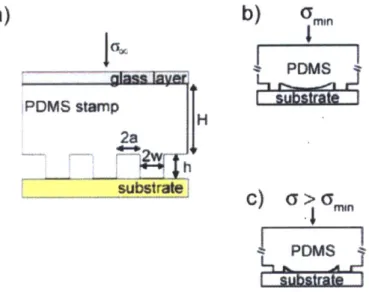
4. Contact Pressure
The required pressure is based on the pressure that can initiate and control conformal
contact. Excessive pressure causes the relief features of the stamp to collapse. In order
to prevent unexpected printing caused by collapse of stamp from excessive force, we
need to consider the basic deformation mechanism. Figure 3.4.4 shows a basic geometry
of a stamp that consists of periodic relief line features with height of h, feature width of
2w, and trench width of 2a. When pressure is applied to the stamp, several deformations
tf
e width of
1000 900 800 700 600 500 -Z*-1occur. These deformations include in-plane lateral expansion, "sagging" of the trench and relief feature from compression by the external stress [21].
a)
b)
07minI
PDMS
stamp
H
2a
substrate
C)
a>a.
4mmFigure 3.4.4: Illustrations of (a) basic geometry of a PDMS stamp and stamps deformed into contact with substrates under (b) required minimum and (c) excess pressures. [30] showed that the height-to-width ratios, the aspect ratios, of the relief structures on PDMS stamps need to be between about 0.2 and 2 in order to obtain defect-free printing. If the aspect ratio of the PDMS feature is too high, the roof of the feature may come into contact with a substrate under its own weight or under an external pressure. When the aspect ratios are too low, the relief structures are
not able to withstand the stamp weight [22].
Specifically, the model for promoted contact between roof and substrates under external stress is suggested by Hui [13] as follows.
Vm = *'" (w+a) cosh~
se
1
" M E' I 2(w +a))
where V,,, is the maximum displacement of the roof by an applied minimum external
stress, and the conformability (i.e. the ratio of Young's modulus divided by the work of
adhesion (or E/w) of the material) was found to be a measure of the spontaneous occurrence of conformal contact as well as of spreading collapse [28].
Another driving force that causes stamp to collapse or driving the conformal contact is the adhesion force. According to the analysis performed by Bietsch and Michel [28] it takes 400 kPa to conform a Sylgard 184 stamp to a surface with 50 nm rms roughness.
However, conformal contact can be achieved under a small force such as the self weight of the stamp. Moreover, K. J. Hsia et al. [23] observed collapse of groove regardless of self-weight or normal force. According to their study, interfacial adhesion force is the main driving force of groove collapse, and they developed a parameter, which is a function of feature width, height, surface energy, and Young's modulus, that determines the adhesion force.
5. The Choice of Inking Method
Inking can be carried out in three different ways - Immersion inking, Pen-Type inking, and Contact inking.
A
B
Ink
Stamp
Ink tank
Printed patter
Figure 3.4.5.1: Three different types of inking for Micro contact printing.
The patterned stamp is consequently inked only via the contact zones where molecules will be needed in step 2. Concentration and immersion time are inversely related: low concentrations of
thiols in solution require long immersion times. (A) A liquid inking technique allows impregnation of the entire surface of the patterned stamp with a drop a dilute solution of thiols in
ethanol. The possible consequence of this inking method is the interference during printing of thiols on the stamp adjacent to the regions of contact. (B) Inking a stamp by transferring thiols from a liquid reserve of alkanethiols in ethanol through the PDMS allows the stamp to be inked permanently and reused readily, but does not localize this stamp impregnation only where needed
(C) Direct inking of the patterned stamp follows its contact with a flat inker pad previously
6. Propagation methods.
Air bubbles trapped between the stamp and substrate easily occur when large areas are
printed. Several methods, such as Micro contact printing under the low pressure
environment [23] and forcing air out using flexible backings have been studied, but
contact initiation and propagation is simple and generally used method.
The contact propagation can be categorized into three methods: radial contact
propagation, linear contact propagation, and rolling contact propagation.
a)
c)
Figure 3.4.5.2: Three contact propagation methods (a) Radial contact propagation (b) Linear contact propagation (c) Rolling contact propagation [23].
Radial contact propagation is done by making a stamp convex. The contact initiation
starts from the center, and convexity is decreased gradually along with spreading contact
region. [16]. Linear contact propagation starts from line contact instead of point contact.
The end of a bent stamp creates line contact initiation and contact area gradually
increases by dropping the stamp gently. A thin bendable layer of metal or polymer can be
used for backing the soft stamp. Third contact propagation method is rolling contact,
using cylindrical stamp. In terms of automation, rolling propagation has benefits in that it does not require another mechanism or process for separation of stamps after printing. Moreover, rolling propagation can simply scalable to mass production process of Micro contact printing such as reel to reel process. However, the deformation of stamp is difficult to expect during preparing cylindrical stamp and printing.
7. Temperature
It has been known that forming SAMs at temperatures above 25*C can improve the kinetics of formation and reduce the number of defects in them [9].Also, the effect of temperature is particularly relevant during the first few minutes of the formation of a
SAM when most of the adsorption and reorganization of the SAM is taking place.
3.5 Summary of manufacturing considerations.
Rate, quality, cost, and flexibility of manufacturing process provide systematic and analytical view not only in evaluation but also in designing the process. Therefore, critical factors related to physics and automation of the process should be considered based on the four factors.
Rate:
In designing an automated Micro contact printing process, it is important to decouple the printing and inking processes such that two processes operate independently or individual processing times.
As discussed in chapter 3.2, different inking methods require different inking time, and printing time mainly depends on two factors, concentration of ink solution and target thickness of SAMs. Because micro contact printing is a serial process involving inking and stamping, the time to complete inking and printing needs to be simulated by deciding
key factors such as inking method and concentration of ink before designing a production line.
- 9
-Quality:
There are a lot of factors that affect printing quality, but the fundamental problems of
Micro contact printing relate to the properties of the stamp material. Xia et al [22]
proposed three main concerns when Micro contact printing is implemented as one of the
micro fabrication process.
1. The shrinkage of PDMS during curing and the swelling of PDMS by a number of
nonpolar organic solvents such as toluene and hexane.
2. The elasticity and thermal expansion of PDMS makes it difficult to get high
accuracy in registration across a large area.
3. The softness of an elastomer limits the aspect ratio
(height offeature / length offeature) of microstructures in PDMS. When the aspect ratio is too high, two posts
can easily stick together (pairing). If the aspect ration is too low, space between
two posts will collapse (sagging)
Paing
Sagging
PDMS PDMS
Figure 3.4.5.3: Schematic illustration of possible deformations of microstructures in the surfaces
of elastomers [26].
Cost:
The expected cost of tool, ink solution, change over time should be considered in
designing & evaluating Micro contact equipment. Usually, tool cost depends on wear of
the tool (PDMS stamp) but wear has not been reported so far, so it is very difficult to
predict the total tooling cost. However, we can minimize the tool cost by minimizingthe
number of tools in the buffer between inking and printing station.
Flexibility:
In a high volume manufacturing process, flexibility of tooling and tool change -over time are important, so Micro contact printing machine should be designed such that it provides a fast tool changing mechanism. In addition, if Micro contact printing machine is used for multilayer micro fabrication, the tool changing mechanism should also provide accurate registration capability.
3.6 Industrial design efforts for Micro contact printing
* Rolling --- C,,H,,SH Ag orAu S i"
I
Microcontact printing SiAMSelective wet etching
Figure 3.6.1: Schematic procedure for conducting pCP with a rolling PDMS stamp [12].
Micro contact printing by rolling is one way to form patterned SAMs at a high speed and, therefore, appropriate for mass production. Younan Xia et al [57] demonstrated that a minimum feature size of -300nm is achievable using a cylindrical stamp of which diameter is approximately ~ 4 cm. 3 inch gold coated wafer (an area of 50 cm2) was used for a substrate and printed at 2cm/sec. (It take 15 seconds to print 3 inch wafer) A single inking can print 4-5 times of printing without showing any difference in terms of defects
in SAMs. The main disadvantage of rolling is that feature on stamp should be deformed to make a cylindrical stamp, which limits the minimum resolution or feature width of pattern.
* Wave printing
7
Figure 3.6.2: A vertical Cross-section of the wave printing prototype [58].
1: Stamp-backplane assembly; 2: Substrate; 3: Working gap (~
100p
jm); 4:Vaccum supply; 5:Pressure supply (z2kPa); 6:Valves switched to pressure supply, thereby creating the wave. 7, 8:Grooves-plate [15].
The concept of wave printing [58] was proposed in order to minimize the deformation and distortion of patterned SAMs printed by the stamp which has both large and small feature and space in a single stamp. Slender posts (height to width ration h/w 2.5) can be easily buckled and sagging will occur if the height of posts is relatively small to space between relief features by a small normal force. In wave printing, a glass backplane as a flexible glass mount is attached to elastomeric stamp to prevent distortion of relief features and this stamp-backplane creates wave by the pressured air mechanism, generating line contact between stamp and backplane. It took twenty minutes for inking, one hour for drying, and 15 seconds for printing as small as 0.75 pm, with hpost=2.3 pm. Micro contact wave printing demonstrated single layer cap4bilities with very low distortions.
3.7 Conclusions
In this chapter, we discussed the process physics and principles behind micro contact printing. The critical factors that determine manufacturability using the process were also discussed besides a few industrial design efforts to automate the process. In the next chapter, we will discuss a manufacturing system that we have designed for commercializing production using micro contact printing. We will also present the design of a prototype to automate the inking and stamping steps.
Chapter 4
Concept Design and Realization
4.1 Introduction
The objectives of this project included designing a manufacturing system for micro contact printing and prototyping an automated system for inking and stamping that could achieve economically viable process. To achieve these goals, a thorough understanding of the process physics involved in micro contact printing was required besides identifying the critical factors that could contribute to output quality and production rate. The final manufacturing system design and the prototype design were derived after several design iterations. The key breakthrough in the design process was achieved on the realization that the target substrate was a flexible sheet of gold coated plastic film which allowed keeping the stamp stationary (to avoid stamp deformation) and apply the substrate onto the stamp while achieving linear propagation (to avoid air bubbles).
This chapter takes the reader through some of the most important design iterations towards the final design. We discuss designs for both the inking and stamping steps. Though some of the designs do not involve the use of a flexible substrate, not only are they are significant milestones in this project but also and can be considered for hard substrates. Finally, we propose a complete manufacturing system for high volume production.
4.2 The Inking Process
Three inking methods are explored and discussed in the academia [5].
1. Wet Inking - Ink is uniformly applied to the PDMS stamp to cover the entire exposed surface area. This is done by fully submerging the patterned surface of the stamp in an ink tub.
2. Pen Stamp - Ink is stored in an ink tank behind the PDMS stamp and diffuses onto the surface of the stamp for stamping. The method derives its name due of its functional similarity to a writing ink pen.
3. Contact Inking - Ink is only applied only to the relief features of the stamp. This is achieved by bringing the stamp's relief feature in contact with a pad soaked
with ink.
Table 4.2 gives a functional comparison for each method.
Wet Inking Pen Stamp Contact Inking Distortion of stamps _____________________swellingCapillary effects, slight Strong swelling No distortion
Adversary diffusion of the Strong NA Strongly minimized
ink (HDT)
Geometric effects Some NA Strongly minimized
Surface crystallization Strong (>=0.5mM) tronmM) Strong (>=0.5mM)
Ease for repeated Bad Very good Fair
inking/printing Bad_ _ery good Fair
Scalability Unknown NA Plausible
Economy of reagent Bad Very Good Fair
Table 4.2 Comparison of Three Methods of Inking Stamps for pCP.
Stamp distortion is important to us since a single stamp may have to go through multiple rounds of printing in the industrial production. Even slight distortion would be dramatically reduces the productivity and product quality collectively.
The scalability is also important to us as the goal is to design a machine good for large scale production. For output quality of the printed patterns, it is important that adversary
diffusion (due to vapor transport) is minimized. With the factors above and Table 4.2, contact inking was chosen be the most appropriate inking method for this project.
4.2.1 Designs for Inking
Having decided upon contact inking for the reasons outlined in section 4.2, several mechanisms to achieve it were considered. The most important ones are described next.
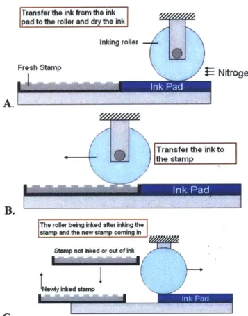
1. Roll Inking
A hard roller is inked by rolling it over an ink-soaked pad (contact inking) or by having an ink tank inside (Pen Inking). Then the roller rolls over a fresh stamp to transfer the ink. The advantage of this design is that it could generate linear propagation (to the ink) during the inking process to apply the ink uniformly over the stamp. Also the inking time between the roller and the stamp could be well controlled by the forward motion of the roller. Thirdly, it's convenient to shift between the stamping inking stage and the inking roller inking stage.
However, there are also several challenges with this design.
1. The vertical position of the inking roller determines the applied pressure. Excessively high pressure may deform the stamp while insufficient pressure may lead to insufficient ink transfer or worse, slippage causing some relief features to miss ink application completely.
2. The weight balance of the roller. As the weight of the roller itself is big enough to cause the deformation of the stamp, the weight must be well balanced with the external mechanism.
3. If applying the wet ink to the stamp, it takes longer to dry the ink. After the stamp is inked, it has to wait for another 10-60 seconds before it can be shifted to the printing. This could be the bottleneck for the process.
![Figure 1.2.1: Schematic illustration of the procedure for fabricating PDMS stamps from a master having relief structures on its surface [3].](https://thumb-eu.123doks.com/thumbv2/123doknet/14681321.559328/11.918.298.609.522.962/figure-schematic-illustration-procedure-fabricating-stamps-structures-surface.webp)
![Figure 2.3.3 shows that the resulting features on the photo resist layer are not as expected by the scalar diffraction theory [18].](https://thumb-eu.123doks.com/thumbv2/123doknet/14681321.559328/25.918.151.751.633.847/figure-resulting-features-resist-expected-scalar-diffraction-theory.webp)
![Figure 3.3: Micro contact printing procedure [16].](https://thumb-eu.123doks.com/thumbv2/123doknet/14681321.559328/33.918.252.643.693.997/figure-micro-contact-printing-procedure.webp)
![Figure 3.4.5.2: Three contact propagation methods (a) Radial contact propagation (b) Linear contact propagation (c) Rolling contact propagation [23].](https://thumb-eu.123doks.com/thumbv2/123doknet/14681321.559328/39.918.203.692.412.742/figure-contact-propagation-methods-propagation-propagation-rolling-propagation.webp)
![Figure 3.6.1: Schematic procedure for conducting pCP with a rolling PDMS stamp [12].](https://thumb-eu.123doks.com/thumbv2/123doknet/14681321.559328/42.918.267.664.321.799/figure-schematic-procedure-conducting-pcp-rolling-pdms-stamp.webp)