HAL Id: hal-03111526
https://hal.archives-ouvertes.fr/hal-03111526
Submitted on 23 Apr 2021
HAL is a multi-disciplinary open access
archive for the deposit and dissemination of
sci-entific research documents, whether they are
pub-lished or not. The documents may come from
teaching and research institutions in France or
abroad, or from public or private research centers.
L’archive ouverte pluridisciplinaire HAL, est
destinée au dépôt et à la diffusion de documents
scientifiques de niveau recherche, publiés ou non,
émanant des établissements d’enseignement et de
recherche français ou étrangers, des laboratoires
publics ou privés.
A multifunctional standardized magnetic tunnel junction
stack embedding sensor, memory and oscillator
functionality
A. Chavent, V. Iurchuk, L. Tillie, Y. Bel, N. Lamard, L. Vila, U. Ebels,
Ricardo C. Sousa, B. Dieny, G. Di Pendina, et al.
To cite this version:
A. Chavent, V. Iurchuk, L. Tillie, Y. Bel, N. Lamard, et al.. A multifunctional standardized
mag-netic tunnel junction stack embedding sensor, memory and oscillator functionality. Journal of
Mag-netism and Magnetic Materials, Elsevier, 2020, 505, pp.166647. �10.1016/j.jmmm.2020.166647�.
�hal-03111526�
A multifunctional standardized magnetic tunnel junction stack embedding
sensor, memory and oscillator functionality
A. Chaventa, V. Iurchuka, L. Tilliea, Y. Bela, N. Lamarda, L. Vilaa, U. Ebelsa, R.C. Sousaa, B. Dienya, G. di Pendinaa,
G. Prenata, J. Langerb, J. Wronab, I.L. Prejbeanua
aUniv. Grenoble Alpes/ CEA / CNRS, Spintec, France bSingulus Technology, Germany
Abstract
The objective of this study is to co-integrate multiple digital and analog functions together within CMOS by devel-oping a universal magnetic tunneling junction stack (MTJ) capable of realizing logic, memory, and analog functions, within a single baseline technology. This will allow monolithic heterogeneous integration, fast and low-power process-ing, and high integration density, particularly useful for Internet of Things (IoT) platforms. This unique spintransfer-torque (STT) MTJ is called Multifunctional Standardized Stack (MSS). This paper presents the progress regarding memory, oscillator and sensor functionalities targeted for the technology. We show that a single magnetic stack deposition can be used to obtain these three functionalities on the same wafer.
1. Introduction
The MTJs are mainly used nowadays for non-volatile memory (STT-MRAM) [1, 2, 3, 4], but also as magnetic sensors [5, 6, 7]. These functionalities in principle require application specific stacks. Heterogeneous inte-gration allows to enhance the functionalities involved through gains in Si footprint area, and new design possibilities. Very recently the same magnetic stack was used to achieve different memory specifications [8]. The novelty of our work is to create entirely different functions: a non-volatile memory bit, an RF-oscillator and a magnetic sensor, based on the same deposited stack. To the best of our knowledge this is the first such attempt to achieve these 3 functionalities. The starting point is interfacial perpendicular magnetic anisotropy (PMA) MTJ, which is now the mainstream technology of STT-MRAM. The strategy then consists in reducing the perpendicular anisotropy to find a working trade-off for all 3 functions.
The principle of the heterogeneous integration here is to have a front end CMOS, with back-end MTJs pro-cessed into pillars. A current is then sent through the MTJ which induces switching or precessional motion of its magnetization under STT. For sensor operation, magnetic flux concentrators will be integrated around the specific MTJs to be used as sensors. Since the MTJ has perpendicular anisotropy, the flux concentrator will
amplify the in-plane field to exploit reversible magne-tization rotation arising when field is applied along the hard axis.
2. Experimental Method
The magnetic stack was developed in a Singulus sputtering tool : [Co 0.5/Pt 0.2]6/Ru 0.8/[Co 0.6/Pt
0.2]3/Ta 0.2/Co 0.9/W 0.25/CoFeB 1/MgO 0.8/CoFeB
x/W 0.3/CoFeB 0.5/MgO 0.75nm, where x = 1.3 nm or 1.4 nm. The reference layer is a compensated synthetic antiferromagnet (SAF). CIPT measurements lead to TMR= 170 % and RA = 7.5 Ωµm2. The stacks
were processed into circular pillars with academic and industrial nanofabrication process flows. At the academic facility, pillars were fabricated using e-beam lithography and ion beam etching (IBE) into diameters from 20 nm to 200 nm, while at the industrial facility they were processed into pillars of diameter 130 nm to 180 nm.
For the characterization of individual MTJ, magneto-resistance measurements were done with a positive volt-age bias of 20 mV. In our sign convention, positive cur-rent or voltage corresponds to electrons flowing from the reference layer to the storage layer.
3. MTJ process characterization
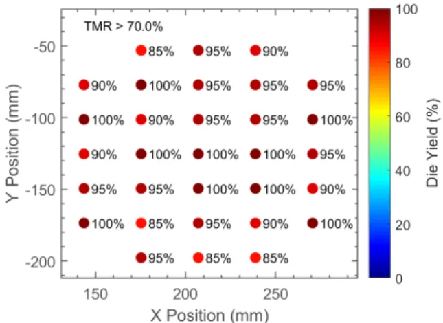
The basic wafer level MTJ parameters: resistance, TMR, coercive and offset fields are measured with an out-of-plane field sweep at 5 Hz after patterning. 20 MTJs per die are measured, and the resulting yield mea-surement on a full wafer map is shown on Fig. 1. The die yield is defined as the percentage of MTJs on a die having a TMR value above 70 %, in agreement with de-sign assumptions for this technology. Most dies have yields above 90 %, with about half of the dies having a single junction out of spec, corresponding to 95 % yield.
Figure 1: Wafer map of the die yield, defined as the yield of each die for a TMR criteria of 70 %.
Figure 2: Magnetoresistance loop of the perpendicular MTJ. HFis the
offset field, HCis the coercive field, Rminand Rmaxare respectively the
resistance in P and AP state.
4. Memory characteristics
To verify memory operation, we characterized the writing behavior using resistance state phase diagrams on individual test cells. The measurement procedure is as follows: the magnetic field is swept continuously, while applying 100 ns voltage pulses at each magnetic field step. The resistance value is measured at 1000 field points along the recorded hysteresis loop, with a voltage of 20 mV. The pulse voltage is varied from 20 mV to 1 V, for both positive and negative values. The measured resistance state is plotted in a diagram as function of field and pulse voltage in Fig. 3.
At a given field of 200 Oe, the high resistance antiparallel (AP) and low resistance state parallel (P) are reached for pulses of 0.7 V respectively with positive and negative voltages. This shows the memory functionality by STT writing, however it requires an external applied field of 200 Oe, to compensate the dipolar coupling field from the reference layer HF
favoring the P state, as shown in Fig. 2. The coupling field can be reduced by changing the SAF reference layer to provide better field compensation without impacting the writing behavior [9]. A second factor prevents writing at zero field, which is the reduction of coercivity above 0.6 V (Fig. 3). The observed affect, can be related to cell heating at higher voltage thereby reducing the anisotropy of the storage layer or to some storage-reference layer interaction reducing the stability of the written state. In any case the best strategy to achieve zero field operation would be to reduce the reference layer dipolar coupling field.
Figure 3: Phase diagram of an MTJ as function of out-of-plane field and voltage amplitude of 100 ns pulses.
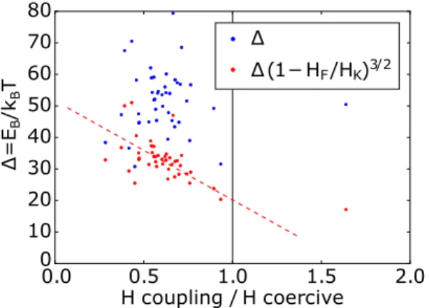
To characterize memory retention for operation as a non volatile memory, we also measured the thermal sta-2
bility barrier∆ = kE
BT. The thermal stability is estimated
from the switching field distribution [10], obtained from 300 hysteresis loop measurements (Fig. 4). Values of∆ are around 40 to 60, which corresponds to a minimum retention of 10 years for one bit, achieving the design requirements of some applications. Due to the coupling field of the reference electrode HF, the AP state is less
stable, and the reduction of stability can be estimated by including a correction coefficient (1 − HF/HK)3/2,
where HKis the anisotropy field of the storage layer, in
the range 1000 Oe to 2000 Oe. The stability of AP state decreases strongly for HF/HC above 0.5, falling below
30, which implies a retention of only a few hours. As previously mentioned, one solution is to reduce the cou-pling field, however a second option is to increase the coercive field without changing the stack.
0.0 0.5 1.0 1.5 2.0 H coupling / H coercive 0 10 20 30 40 50 60 70 80 ∆ =E B /kB T ∆ ∆(1− HF/HK)3/2
Figure 4: The stability∆ as function of the ration HF/HCbetween the
coupling field and the coercive field.∆(1 − HF/HK)3/2is the stability
of the AP state.∆ and HKare estimated by fitting the switching field
distribution.
This can be achieved by reducing the pillar diameter through a trimming process by ion beam etching at a grazing angle. Since the ion beam etch is highly direc-tional, the grazing etch angle increases the pillar lateral etch rate (horizontal etch component), while reducing at the same time the vertical etch rate.
The amount of lateral trimming was controlled through time, using longer etch times to achieve stronger trimming of the patterned pillars. For strong trimming conditions, the cell diameter is confirmed to decrease. This is shown is shown in Fig. 5, where samples having strong trimming show effective pillar diameters that are reduced, compared to short trimming conditions. At the same time the coercive field HC
of the storage layer of smaller cells also increases. One possible explanation for this increase, is that the
magnetization reversal mechanism in interfacial PMA MTJ is the nucleation of a domain wall (DW) at pillar edge and its subsequent propagation [11]. The increase of coercive field through trimming would then result from the reduction of DW nucleation sites on the reduced cell area and circumference.
The increase of coercive field reduces the impact of the reference layer coupling field. In fact, as shown in Fig. 5, the ratio between the coupling field and the co-ercive field is below one in the case of strong trimming. It means that the trimming only increased the coercive field, but not the coupling field. Having this ratio below one allows zero field operation.
The STT efficiency was calculated assuming ∆ = 70kBT, an average switching voltage of 0.5 V and RA=
7.5Ωµm2, resulting in 1.5 k
BT/µA for a 30 nm
diam-eter device, which is about half the efficiency reported for comparable state-of-the art stacks [10].
Diameter (nm) Co e rc ive fi e ld Hc ( Oe ) 0 50 100 150 200 0 200 400 600 800 1000 1200 1400 0 50 100 150 200 Diameter (nm) 0.0 0.5 1.0 1.5 2.0 H co up ling /c o e rc ive Low trimming Strong trimming
Figure 5: Left : Coercive field. Right : Ratio between coupling and coercive field, which depicts the stability in zero field. The data are shown for low or strong trimming during the IBE etching, as function of diameter calculated from electrical resistance and RA.
5. Sensor functionality
The basic principle for magnetic field sensor opera-tion is for the field to induce a change of the angle α be-tween the reference and the storage/sensing layer mag-netization direction. This result in a resistance change the according following relationship [12]:
G(α)=GP+ GAP
2 +
GP− GAP
2 cos(α) (1)
Where G= 1/R is the conductance, R the resistance, GPand GAPthe conductance in the P and AP state.
Various sensor applications exist with their own specific requirements. Here the objective was to have a reversible dependence with low hysteresis, allowing for the measurement of one single magnetic field
component.
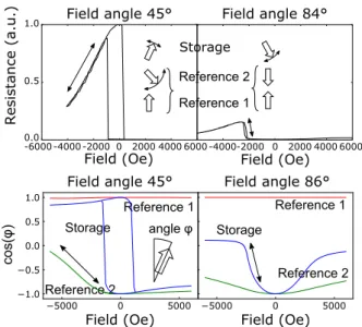
To identify field ranges with possible sensor op-eration, we measured magnetoresistance loops for various angles θ of the field with respect to the easy axis orthogonal to the wafer plane, as shown in Fig. 6. Hysteretic switching of the storage layer along its anisotropy axis is observed at measured field angles below θ= 80◦. For θ= 45◦, starting in the AP state, the resistance varies reversibly on a range of a few thousand Oersted. This behavior is reversible and corresponds to a first scenario of magnetic sensor functionality. For θ around 85◦, the main hysteresis field range disappears, and is replaced by reversible resistance change around the P state, corresponding to a second possible sensing scenario providing larger sensitivity on a narrower range of fields.
Figure 6: Magnetoresistance loops of a perpendicular MTJ with the stack where the CoFeB thickness x is 1.4 nm. The loops are measured for various angles of the field with respect to the normal to the wafer.
To better understand these behaviors and verify whether further improvements are possible, we made a macrospin energy model, illustrated on Fig. 7. It allows for the calculation of the magnetization angle φ of each layer as a function of applied magnetic field. For scenario 1 with θ= 45◦, the angle φ of the storage layer almost does not change within the sensing field range. The change of resistance through the angle α is mainly due to the rotation of the top part of the reference (Reference 2). For the scenario 2 with θ = 84◦, the
closest behavior with the same parameters of the model was obtained assuming a field angle of θ= 86◦. In that
case, the reference layer (Reference 2) slowly rotates on a large field range of a few thousand Oe as previously. However, it is the reversible rotation of the storage
layer around 2000 Oe which is actually responsible for the largest resistance change observed in the second sensing scenario. angle φ 5000 0 5000 Field (Oe) Field angle 86° Reference 1 Reference 2 Storage Reference 1 Reference 2 Storage 5000 0 5000 Field (Oe) 1.0 0.5 0.0 0.5 1.0 Field angle 45° cos( φ ) Reference 2 Reference 1 Field (Oe) Field angle 45° -6000 -4000 -2000 0 2000 4000 6000 0.0 0.5 1.0 Resista nce (a.u.) Field (Oe) Field angle 84° -4000-2000 0 2000 4000 6000 Storage
Figure 7: Top : measurement taken from 6. Bottom : angle φ of each layer of the stack in a macrospin energy model. Left : scenario 1 with sensing around the AP state. Right : scenario 2 with sensing around the P state.
5.1. Flux concentrator
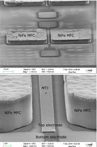
Magnetic flux concentrators (MFC) were integrated on the MTJs aimed at demonstrating sensor func-tionality for two reasons. The first is to increase the sensitivity, the second one is to achieve the overlap the operating field window for memory and sensor operation. These flux concentrators are made of electrodeposited NiFe, as shown on Fig. 8. Table 1 summarizes the properties of various flux concentrator geometries fabricated for different values of the thick-ness and gap.
5.2. Flux concentrator characterization
To characterize the efficiency of the MFC, the in-plane field required to switch the storage layer, as in sensing scenario 2, was compared with and without flux concentrators. The uncertainty associated to this calibration procedure is that the field within the gap of the flux concentrators, at the MTJ level, might be tilted compared to the external magnetic field axis leading to changes in switching field (θ = 80◦ and θ= 84◦on
Fig. 6). Fortunately, the field tilt is linked to the angle 4
NiFe MFC NiFe MFC MTJ Top electrode Bottom electrode NiFe MFC NiFe MFC
Figure 8: SEM image of the MTJ with MFC integrated.
α, which can be deduced from the magneto-resistance. The field amplification factor is given in the table 1. The best factor is 6, and is obtained for large Thick-ness/Gap ratio of 0.9, in agreement with literature [13]. We also made variations of the MFC shape, but differ-ences between them are within the experimental error.
Thickness 2.5 µm 2.5 µm 4.5 µm
Gap 5 µm 11 µm 5 µm
Thickness/Gap 0.5 0.2 0.9
Amplification Factor 3.4 2.3 6
Table 1: MFC characteristics and measured field amplification factor of the MFC integrated MTJ.
5.3. Sensor characterization
The sensor sensitivity of the MTJ with MFC integrated was characterized. In Fig. 9, the magnetore-sistance curve with and without MFC are compared.
In the case of an out-of-plane field, the sensing sce-nario 1 can be applied, showing a reversible change of resistance of the AP state over a field range of 3000 Oe. The sensitivity of this sensing scenario is clearly improved by the use of an MFC. The resulting magnetoresistance loop is similar to that of Fig. 7 without MFC, assuming θ = 45◦, even though the
external field is applied out-of-plane. This is probably due to a small in-plane field component arising from the flux concentrators. In the case of in-plane field, without MFC, no change of resistance can be seen on the ±1000 Oe field range. However, using MFC in the sensing scenario 2 configuration, a reversible resistance change of around 500 Oe can be observed. This field value can be compared with the 2000 Oe obtained without MFC (Fig. 7, θ = 84◦). The MFC clearly allows to bring the sensor field window closer to the memory working field window.
1000 500 0 500 1000 In Plane Field (Oe) 3000 1500 0 1500
Out Of Plane Field (Oe) 1000 1600 2200 2800 Re si sta nc e ( ) Without MFC With MFC MFC MFC MFC MFC
Figure 9: Sensing tests with and without the MFC integrated.
The sensitivity of various samples in both scenarios is summarized in table 3. The sensitivity was mea-sured for a DC bias voltage of 30 mV and estimated at 400 mV by taking into account the dependence of resistance with bias voltage which are give by : V : RAP/RAP0= 1−0.6V and RP/RP0= 1−0.04V. The
sen-sitivity obtained in the scenario 2 compares well with those of standard dedicated FeCoB/MgO/FeCoB MTJ. For example in reference [7] a sensitivity of 39 V/T is reported on a few tens of Oersted. The main difference in our case is the offset of 500 Oe, that would have to be taken into account for the application. Further examples are discussed in a recent review paper on magnetoresis-tance (MR) sensors[14], highlighting how different MR technologies can be applied in specific sensing tasks.
scenario 1 scenario 2 Field angle θ 10 to 20◦ 80 to 90◦ Sensitivity 0.05 to 0.08 %/mT 1 to 10 %/mT 0.15 to 0.25 V/T 4 to 40 V/T Offset 1000 Oe 500 Oe Range 1500 Oe 50 Oe
Table 2: Sensor characteristics in both scenario. The sensitivity in unit V/T, was estimated with a bias voltage of 400 mV.
Perpendicular In-plane Field angle θ 10 to 45◦ 80 to 90◦
Sensitivity 0.05 to 0.08 %/mT 1 to 10 %/mT 0.15 to 0.25 V/T 4 to 40 V/T
Range 1500 Oe 50 Oe
Table 3: Sensor characteristics in both scenario. The sensitivity in unit V/T, was estimated with a bias voltage of 400 mV.
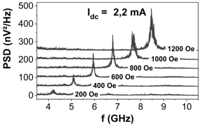
6. Oscillator characteristics
Spin torque oscillators allow for radio frequency (RF) functionality, in a frequency range of 1-20 GHz. Various RF functionalities were explored, such as gen-eration, detection and modulation. For RF gengen-eration, as an example, the principle is to apply a DC current to the MTJ, such that it exerts a torque on the storage layer by STT, which will trigger sustained oscillations. These magnetization oscillations yield oscillations of the MTJ resistance which consequently emits an RF current.
For the measurement shown in Fig. 10, an in-plane field is applied, with positive applied current flow-ing through the MTJ, while the power spectral density (PSD) is measured as a function of the frequency. There is a clear peak in the PSD due to RF oscillation. It ap-pears more clearly with positive current polarity. In fact, as shown in Fig. 6, with an in-plane field, it is not pos-sible to obtain an AP state, and the oscillations appear around the P state resistance level. The positive current is supposed to stabilize the storage layer in the P state instead of triggering oscillations. The more likely ex-planation is therefore that the reference layer oscillates due to the positive current destabilizing the P state ref-erence layer direction.
The generation was characterized for two configura-tions, one using in-plane field and the other out-of-plane field. The performance parameters for signal genera-tion are the emission linewidth and the generated output power, that are summarized in table 4 for both field ori-entations. As can be seen for out-of plane field much
Figure 10: Spectrum of the RF response to a DC current, with in-plane field
better performances were achieved with a linewidth of 20 MHz and a power of 20 nW. These values are in the range in-plane magnetized MTJ devices [15] and will allow testing further functionalities such as injec-tion locking, modulainjec-tion or inserinjec-tion into a Phaselocked loop (PLL) for frequency synthesis. Experiments on this are currently ongoing using our previously devel-oped hybrid CMOS-PCB PLL circuit [16].
The frequency, linewidth and power emission are summarized in table 4. It is possible that these two configurations correspond to the sensing scenarios de-scribed above. In the configuration of in-plane field, the linewidth 100 MHz is too large, and the power 0.8 nW is too low to allow its use coupled to a phase locked loop (PLL), the basic block of a RF synthesis circuit. On the contrary, with out-of-plane field, the linewidth 20 MHz and the power 20 nW are compatible with PLL requirements.
Field In-plane 800 Oe Out-of-plane 2200 Oe Frequency 5 to 9 GHz 3 to 5 GHz
Linewidth 100 MHz 20 MHz
Power 0.8 nW 20 nW
Table 4: Generation characteristics of the MSS in two magnetic field configurations.
7. Conclusion
We have verified the functionality of storage, field sensing and RF generation of magnetic tunnel junctions fabricated with the same perpendicular MTJ stack.For memory applications, STT writing was confirmed on devices having an energy barrier compatible with 10 year bit retention. Achieving zero field operation still requires a reduction of the reference layer dipolar 6
coupling field, that can be achieved by reducing the magnetic moment of the thicker Co/Pt multilayer SAF structure. For sensing, two scenarios are possible, one on a large field range with low sensitivity, the other on a narrower field range with high sensitivity. We also report RF generation with characteristics compatible with CMOS integration.
This work has received funding from the European Union’s Horizon 2020 research and innovation program under grant GREAT No. 687973 and ERC Advanced Grant MAGICAL No. 669204.
References
[1] O. Golonzka, J. G. Alzate, U. Arslan, M. Bohr, P. Bai, J. Brock-man, B. Buford, C. Connor, N. Das, B. Doyle, et al., Mram as embedded non-volatile memory solution for 22ffl finfet tech-nology, in: 2018 IEEE International Electron Devices Meeting (IEDM), 2018, pp. 18.1.1–18.1.4. doi:10.1109/IEDM.2018. 8614620.
[2] S.-W. Chung, T. Kishi, J. W. Park, M. Yoshikawa, K. S. Park, T. Nagase, K. Sunouchi, H. Kanaya, G. C. Kim, K. Noma, et al., 4gbit density stt-mram using perpendicular mtj realized with compact cell structure, in: 2016 IEEE International Elec-tron Devices Meeting (IEDM), 2016, pp. 27.1.1–27.1.4. doi: 10.1109/IEDM.2016.7838490.
[3] Y. J. Song, J. H. Lee, H. C. Shin, K. H. Lee, K. Suh, J. R. Kang, S. S. Pyo, H. T. Jung, S. H. Hwang, G. H. Koh, et al., Highly functional and reliable 8mb stt-mram embedded in 28nm logic, in: 2016 IEEE International Electron Devices Meeting (IEDM), 2016, pp. 27.2.1–27.2.4. doi:10.1109/IEDM.2016. 7838491.
[4] J. J. Nowak, R. P. Robertazzi, J. Z. Sun, G. Hu, J. Park, J. Lee, A. J. Annunziata, G. P. Lauer, R. Kothandaraman, E. J. O’Sullivan, P. L. Trouilloud, Y. Kim, D. C. Worledge, Depen-dence of voltage and size on write error rates in spin-transfer torque magnetic random-access memory, IEEE Magnetics Let-ters 7 (2016) 1–4. doi:10.1109/LMAG.2016.2539256. [5] A. Bocheux, C. Cavoit, M. Mouchel, C. Ducruet, R. Fons,
P. Sabon, I.-L. Prejbeanu, C. Baraduc, High sensitivity mag-netic field sensor for spatial applications, in: 2016 IEEE Sensors Applications Symposium (SAS), 2016, p. 1–5. doi:10.1109/ SAS.2016.7479836.
[6] M. Mouchel, A. Bocheux, C. Ducruet, P. Sabon, I.-L. Prejbeanu, Y. Conraux, J. Alvarez-H´erault, K. Mackay, C. Baraduc, Noise study of magnetic field sensors based on magnetic tunnel junc-tions, Journal of Physics: Conference Series 903 (2017) 012008. doi:10.1088/1742-6596/903/1/012008.
[7] M. Dabek, P. Wisniowski, T. Stobiecki, J. Wrona, S. Cardoso, P. P. Freitas, Sensitivity and 3 db bandwidth in single and series-connected tunneling magnetoresistive sensors, Sensors 16 (11) (2016). doi:10.3390/s16111821.
[8] J.-H. Park, J. Lee, J. Jeong, U. Pi, W. Kim, S. Lee, E. Noh, K. Kim, W. C. Lim, et al., A novel integration of stt-mram for on-chip hybrid memory by utilizing non-volatility modulation, in: 2019 IEEE International Electron Devices Meeting (IEDM), 2019, p. (in press).
[9] S. Bandiera, R. C. Sousa, Y. Dahmane, C. Ducruet, C. Porte-mont, V. Baltz, S. Auffret, I. L. Prejbeanu, B. Dieny, Com-parison of synthetic antiferromagnets and hard ferromagnets
as reference layer in magnetic tunnel junctions with perpen-dicular magnetic anisotropy, IEEE Magnetics Letters 1 (2010) 3000204–3000204. doi:10.1109/LMAG.2010.2052238. [10] L. Thomas, G. Jan, J. Zhu, H. Liu, Y.-J. Lee, S. Le, R.-Y. Tong,
K. Pi, Y.-J. Wang, D. Shen, R. He, J. Haq, J. Teng, V. Lam, K. Huang, T. Zhong, T. Torng, P.-K. Wang, Perpendicular spin transfer torque magnetic random access memories with high spin torque efficiency and thermal stability for embedded ap-plications (invited), Journal of Applied Physics 115 (17) (2014) 172615. doi:10.1063/1.4870917.
[11] T. Devolder, J. Kim, J. Swerts, S. Couet, S. Rao, W. Kim, S. Mertens, G. Kar, V. Nikitin, Material developments and do-main wall-based nanosecond-scale switching process in per-pendicularly magnetized stt-mram cells, IEEE Transactions on Magnetics 54 (2) (2018) 1–9. doi:10.1109/TMAG.2017. 2739187.
[12] J. C. Slonczewski, Conductance and exchange coupling of two ferromagnets separated by a tunneling barrier, Phys. Rev. B 39 (1989) 6995–7002. doi:10.1103/PhysRevB.39.6995. [13] X. Sun, L. Jiang, P. Pong, Magnetic flux concentration at
mi-crometer scale, Microelectronic Engineering 111 (2013) 77–81. doi:10.1016/j.mee.2013.01.063.
[14] S. Cardoso, D. C. Leitao, T. M. Dias, J. Valadeiro, M. D. Silva, A. Chicharo, V. Silverio, J. Gaspar, P. P. Freitas, Challenges and trends in magnetic sensor integration with microfluidics for biomedical applications, Journal of Physics D: Applied Physics 50 (21) (2017) 213001. doi:10.1088/1361-6463/aa66ec. [15] A. Ruiz-Calaforra, A. Purbawati, T. Br¨acher, J. Hem, C.
Mu-rapaka, E. Jim´enez, D. Mauri, A. Zeltser, J. A. Katine, M.-C. Cyrille, et al., Frequency shift keying by current modulation in a mtj-based stno with high data rate, Applied Physics Letters 111 (8) (2017) 082401. doi:10.1063/1.4994892.
[16] M. Kreißig, R. Lebrun, F. Protze, K. J. Merazzo, J. Hem, L. Vila, R. Ferreira, M. C. Cyrille, F. Ellinger, V. Cros, et al., Vor-tex spin-torque oscillator stabilized by phase locked loop us-ing integrated circuits, AIP Advances 7 (5) (2017) 056653. doi:10.1063/1.4976337.