Clock Division as a Power Saving Strategy in a
System Constrained by High Transmission
Frequency and Low Data Rate
by
Andrew D. Selbst
Submitted to the Department of Electrical Engineering and Computer
Science
in partial fulfillment of the requirements for the degree of
Masters of Engineering in Electical Engineering and Computer Science
at the
MASSACHUSETTS INSTITUTE OF TECHNOLOGY
June 2005
@
Massachusetts Institute of Technology 2005. All ri hts reserved.
OF TECHNOLOGY
JUL
18
2005
Author...
UBRAR.IES
Department of Electrical Engineering and Computer Science
May 20, 2005
Certified by...
Rahul Sarpeshkar
Associate Professor, Electrical Engineering and Computer Science
Thesis Supervisor
Accepted by.
....
...
Arthur C. Smith
Chairman, Department Committee on Graduate Students
Clock Division as a Power Saving Strategy in a System
Constrained by High Transmission Frequency and Low Data
Rate
by
Andrew D. Selbst
Submitted to the Department of Electrical Engineering and Computer Science on May 19, 2005, in partial fulfillment of the
requirements for the degree of
Masters of Engineering in Electrical Engineering and Computer Science
Abstract
Systems are often restricted to have higher transmission frequency than required by their data rates. Possible constraints include channel attenuation, power require-ments, and backward compatibility. As a result these systems have unused band-width, leading to inefficient use of power. In this thesis, I propose to slow the internal operating frequency of a cochlear implant receiver in order to reduce the internal power consumption by more than a factor of ten. I have created a new data encoding scheme, called "N-7r Shift Encoding", which makes clock division a viable solution. This clock division technique can be applied to other similarly constrained systems. Thesis Supervisor: Rahul Sarpeshkar
Acknowledgments
I would like to acknowledge my supervisor, Rahul Sarpeshkar, for providing me with
funding and numerous chances at redemption so that I could write this thesis. I would also like to acknowledge everyone in the Analog VLSI and Biological Systems Group at MIT for sharing their time and knowledge when I revealed my inexperience. I would especially like to thank Soumyajit Mandal, who laughed at me when I thought
I had to defy the laws of physics, Michael Baker, who eased me into the group and likely preserved my future sanity without knowing it at the time, and Micah O'Halloran for some emergency editing when I wasn't even able to think straight. I would like to thank fellow M.Eng student Colin Weltin-Wu for his conversations with me about PLLs, including the original version of the phase detector I eventually used. I would also like to thank my friend, Andrew C. Thomas, a Ph.D student in Statistics at Harvard University, for his help verifying the uniform probability density of the circular random walk. Finally, I would like to thank Vera Sayzew, Anne Hunter, and Professor Art Smith in the Course VI Undergraduate Office, for making me feel like
Contents
1 Introduction
1.1 Origins of the Project. . . . .
1.2 Low Power and Implantable Devices .
1.3 Cochlear Implants . . . .
1.4 Receiver Requirements . . . .
2 Transmission Constraints
2.1 Channel Characteristics . . . .
2.1.1 Frequency Specific Attenuation
2.2 Power Constraints . . . .
2.3 Practical Considerations . . . .
2.4 Required Bandwidth . . . .
3 Binary PSK Receiver
3.1 Phase Locked Loop ...
3.1.1 Manchester Encoding . . . .
3.1.2 Duty Cycle Phase Detector . . 3.1.3 Charge Pump . . . .
3.1.4 Loop Filter and VCO . . . .
3.1.5 PLL performance . . . .
3.2 Power Supply and Data Recovery . . .
3.2.1 Power Supply . . . . 3.2.2 Data Recovery . . . . 13 . . . . 14 . . . . 14 . . . . 15 . . . . 16 19 19 19 20 20 21 23 24 25 26 29 29 31 32 32 33
4 Clock Division and Its Consequences
4.1 Detection Difficulties . . . .
4.1.1 Short Pulse Output . . . .
4.1.2 More Than One Possible Output
4.2 Phase Transitions and the Random Walk
5 N-r 5.1 5.2 5.3 5.4 Shift Encoding
Adding N7r To the Phase . . . . Simple Digital Implementation . . . .
Transmission of an Encoded Signal . . .
Conclusions and Future Work . . . .
A Discussion of the Circular Random Walk
37 39 39 40 44 47 . . . . 4 9 . . . . 5 1 . . . . 5 4 . . . . 5 6 59
List of Figures
3-1 BPSK Receiver Block Diagram . . . . 23
3-2 Block Diagram of CDR PLL . . . . 24
3-3 A Demonstration of Manchester Encoding. The original data (top) is
multiplied by a square wave at frequency equal to the data rate , rd.
In the Manchester Encoded data (bottom), a logical "0" is represented
by "01" and a "1" is represented by "10". The dashed lines are the bit
boundaries. . . . . 25
3-4 Nonlinear Phase Characteristics of Two Phase Detectors (Dead Zones
Exaggerated for Illustration) . . . . 27
3-5 Duty Cycle Phase Detector. The local oscillator and reference inputs
are compared and the outputs, Up and Down are sent through equal
delays. . . . . 28
3-6 Differential Charge Pump. Redirects charging and discharging currents
between the two branches. Top and bottom half are independent. Nodes 1 and 2 stay nearly constant due to the differential nature of
the circuit. Iout connects to the loop filter charging capacitor. ... 30
3-7 Third order loop filter designed by Lee's "cookbook" method. All poles
except one are beyond crossover . . . . . 31
3-8 Ghovanloo and Najafi's rectifier. The extra PMOS transistors set the
well potential to the highest point. This reduces the gain of parasitic bipolars, and thus reduces latchup [3]. The measure M is the equivalent
3-9 2V Voltage Regulator. The current reference sets Vn and sets VDD = V" + VP.
The voltage regulator portion turns the shunt transistor on if Vn ' VP.
This in turns burns more current through VDD, changing VP and com-pleting the feedback loop. The capacitors in the current reference are for startup and filtering, and the capacitors in the regulator are for
com pensation. . . . . 34
3-10 An XOR gate decodes BPSK data by comparing the clock (top) and a
encoded signal (middle). The resulting waveform (bottom) is exactly
the data... ... .... ... .. 35
4-1 BPSK Receiver Block Diagram. The clock divider has been added.
This is the complete block diagram. . . . . 38
4-2 The data (top) lags the clock (bottom) by r/16 in phase to represent
a "l" . . . . . 40
4-3 Accumulation of Divided Phase. Several waveforms are presented to illustrate how divided phase is accumulated on each data transition.
These waveforms depict an N = 4 case, with two data transitions at
the arrows. The data and carrier are then divided and the XOR output is the phase difference. XOR.out shows that by switching data twice,
the phase difference increases first to r/N and then again to 27r/N. . 42
4-4 The limiting threshold in the divider is uneven. As a result, inversions
do not always add an edge, but sometimes remove them. The sine wave does not cross the threshold due to the inversion, and as a result,
the limited signal is delayed rather than advanced. . . . . 43
5-1 Demonstration of the phase counting model of edge detection. The
change in data (thick dashed line) causes either an addition or
sub-traction of 7r by adding or subtracting edges compared to the clock
(not shown). The expected falling edge is marked by the thin dashed
5-2 On the data transition (top), the encoded signal (bottom) skips 16
edges, or 8 full cycles . . . . . 50
5-3 Block Diagram of N-r Shift Encoder . . . . 52
5-4 N-7 Shift Encoder. Takes data in and outputs the digital waveform
with N edges skipped. Needs to be filtered before transmission. . . . 52
5-5 N-ir Shift Encoder Internal Waveforms . . . . 53
5-6 FFT of N-7r Shift Encoded Waveform. Most of the energy is contained
at or below 27.12MHZ. This makes it easy to low-pass filter the data
Chapter 1
Introduction
I have designed a cochlear implant receiver which uses clock division to reduce its power consumption by more than a factor of ten. This power reduction takes advan-tage of the fact that power is often wasted in unused bandwidth, and merely cuts down the bandwidth so that less excess power is required. In this thesis, I discuss the receiver as an example of this power reduction technique, though the technique can be used in any system constrained in a similar fashion. The rest of this chapter provides the background necessary to understand and motivate the design of the receiver.
Chapter two discusses several reasons for which a system can be constrained to have a much higher transmission frequency than data rate, and thus motivates clock division as a more widely applicable power solution than just to the receiver.
Chapter three details the implementation and operation of the original receiver, before clock division is applied to reduce power.
Chapter four discusses the effects of clock division on the system, as well as prob-lems that arise when clock division is applied directly, with a straightforward binary phase-shift keyed (BPSK) encoding scheme.
Chapter five describes what I call "N-ir Shift Encoding", the solution that makes clock division possible. I also provide a simple digital implementation of the encod-ing. Finally, I perform a frequency analysis to show that the carrier signal is not significantly disturbed by this encoding scheme and that high-Q transmission is still possible.
1.1
Origins of the Project
The original focus of this project was to build a low power cochlear implant receiver.
I was given the constraint that the data would be BPSK encoded, and PSK signals
require a coherent decoder, as I discuss further in Chapter 3. In general, coherent receivers burn much more power than non-coherent receivers and the power specifi-cation was that the system should run under 100uW total. When the initial PLL design exceeded the power spec by itself, I realized that the easiest way to cut down the power was to reduce the internal operating frequency of the system. The chapters in this thesis approximately coincide with the chronological evolution of clock division as a power saving strategy. As such, the relevant background for this project is that of the receiver itself, rather than clock division. Understanding this background will lead to an understanding of both the need and application of clock division.
1.2
Low Power and Implantable Devices
A large body of research throughout electrical engineering is dedicated to reducing
power consumption in systems. Lower power means lower energy costs for large sys-tems. It is very important in computer processors, to prevent overheating. The field with the largest stake in the research, however, is portable electronics, like laptops, audio devices, and especially biological implants.
The drive toward lower power is fueled by the need for longer lasting and smaller batteries. This is especially critical for biological implants, which cannot occupy much space or be replaced easily. Surgery once every ten years is really the lowest acceptable level of battery life for implants. Since typical rechargeable batteries can be recharged on the order of 500-1000 times, each charge must last at least 3.65 days in the best case.
Assuming cost is not an object in implants, and since space is at such a premium, many implants will use lithium-ion batteries, since they have the highest energy density of the commercially available batteries. The energy density of lithium-ion
batteries is 200 Watt-hours/liter, and a typical pacemaker uses about 10mL on the
battery [6]. That equates to 2 Watt-hours per charge, meaning that if the device
takes even 20mW, the charge will last only 4 days, very near the best-case acceptable limit.
Cochlear implants, on the other hand, are significantly smaller than pacemakers and defibrillators. Currently, they require external batteries and processors because they have only the space between the skull and skin be implanted. However, with new advances in battery design, very flat batteries will fit there, but the implant will
need to be very low power (~ 500pW) to run for the required time. When that mark
is achieved, in addition to a measure of compactness, the system can become fully implantable. My receiver is part of a fully implantable system (FIS), and should therefore use less than 1OOW even when combined with the transmitter. Since the receiver should be able to rectify the incoming signal as its power source, this really sets the limit for the transmitter power, which will be greater than the receiver power due to losses in transmission.
1.3
Cochlear Implants
It is important to understand the motivation for building a working FIS. First, remov-ing the system to recharge the battery every night, as most current cochlear implant patients do, is not an ideal solution. A FIS should require no additional thought once implanted, except the occasional wireless recharge. In addition, it requires only one piece and no wires, so there are fewer pieces to break.
Second, and perhaps more important, is the social aspect of the FIS. There is a stigma associated with being deaf, even if the cochlear implant "repairs" the damaged ear. With a behind-the-ear (BTE) system, the implant is obvious, but a FIS will only manifest itself as a small bump behind the ear, usually covered by hair. This way, cochlear implant patients will more easily integrate into society, with no stigma attached.
distinc-tion between my receiver and the one in the current cochlear implant technology. In the current standard, a microphone is placed inside the ear, and the signal is sent to the BTE signal processor. The battery is also contained in the BTE unit. The signal processor then outputs spectral envelope information, used to stimulate the appro-priate electrodes in the cochlea. The stimulation information is sent via wireless link from the BTE unit to the implant, and then the proper electrodes are stimulated.
In a FIS, the processor is implanted, so the stimulation information is sent directly to the electrodes. However, the microphone is still embedded inside the ear, since it cannot be implanted; the skin muffles the sound too much to be clear. Thus the data sent over the wireless link is compressed audio data, rather than stimulation data. The main implementation difference is an increase in data rate, but to figure out the correct rate, it is important to understand that the receiver is capturing audio data. For reasons discussed extensively in Chapter 2, both types of receivers have carrier
frequency fo = 27.12MHz, but a much lower data rate.
1.4
Receiver Requirements
A cochlear implant's function is to recover speech, so it is not important to include
the entire audio spectrum in the data. In order to preserve all the components of speech, the data needs about a 5kHz bandwidth [5]. If the cutoff comes earlier, it may not be possible to hear the correct sibilants, and an "s" could very well sound like an "f ". Therefore the sample rate was set to 10kHz, giving a bandwidth of 5kHz, and retaining all the important speech information.
The only part of the FIS front end to come before the transmitter is the data compression. The audio data has a dynamic range of about 80dB to start, and the compression reduces that to a 60dB internal dynamic range before sending the data across the wireless link. 60dB of data quantizes to about 10 bits per sample. At 10kHz
sampling, the data rate rd for my system is 100kbps. Due to Manchester Encoding,
which I discuss in Section 3.1.1, the data rate doubles to 200kbps. Since one data bit is one whole period of the associated clock, the fastest the data can switch is
rd/2. Thus the upper frequency bound is only 100kHz, which still resides within the allotted bandwidth of 163kHz (see Section 2.3). Some of the energy in the data does exist outside of the bandwidth, but the peaks are about 30dB below the main peak.
In the next chapter, I motivate clock division specifically, but this background should help to understand why this system is important in its own right, and how it is supposed to work. I discuss the specific implementation thoroughly in Chapter 3.
Chapter 2
Transmission Constraints
The cochlear implant receives data at rd = 100kpbs, fo = 27.12MHz. The
trans-mission frequency, therefore, is almost 2.5 orders of magnitude greater than the data
rate. It is exactly the ratio L that motivates the need for this project. The followingrd
discussion of the restrictions should also make it clear that the same technique can be applied applied to an entire class of systems with similar constraints.
2.1
Channel Characteristics
The first and often most important constraint on fo is that of the channel. Features of different channels can vary greatly, and researchers spend significant amounts of time characterizing them. In the cochlear implant, as with most wireless systems, the transmission channel is just a medium, such as air or water. Other systems use various waveguides, such as transmission lines or coaxial cable, and have very different properties.
2.1.1
Frequency Specific Attenuation
A channel can be viewed as a complicated filter, usually with a gain much smaller
than unity. Often these filters have resonances or notches which will change the gain significantly at only certain frequencies. The easiest example is for any wireless
channel. Without a common ground, DC energy cannot pass through, so all wireless channels cut out very low frequencies.
Some parts of the channel can be designed, such as a high-Q band-pass filter at the receiver's front end. However, some channel properties cannot be accounted for, like the clouds for radio, or the resonances due to the laboratory walls, or the attenuation of a flap of skin for cochlear implants. These considerations often determine the desirable transmission frequencies to within a certain range. Cochlear implants are designed to operate in the tens of megahertz because that is fast enough that a thin flap of skin will look transparent to it, but slow enough so there is not too much power burned in transmission and reception.
2.2
Power Constraints
A second important physical consideration is power consumption. Since the overall
goal of the project is to lower power consumption, it makes sense to lower fo as much as possible. If not for the other constraints then, this would be the solution, and this thesis would be uninteresting.
There is one situation when power actually requires a system to have a higher transmission frequency. Some wireless systems, including the one in this thesis, rectify the incoming signal to power the circuits. Low frequency carriers are difficult to rectify because the capacitors must be very large in order to hold the peak value long enough. An integrated rectifier, however, cannot reasonably have capacitors greater than nF, so low frequency carriers are impractical.
2.3
Practical Considerations
Two of the constraints on the transmission frequency are not physical, but rather are imposed by the government or by industry. The FCC regulates the use of bandwidth for broadcasting, and has allocated certain bands for industrial, scientific, and med-ical applications (ISM bands). Because the cochlear implant falls into each of those
categories nicely, it was important that I stayed within an ISM band. The band I used is centered at 27.12MHz, and has a bandwidth of 163kHz. Some other ISM bands exist at 6.78MHz, 13.56MHz, and 40.68MHz, all of varying bandwidths. For
further band allocations, see [7]. All systems that broadcast fall into some particular
set of frequency bands which are pre-allocated by the FCC.
The second practical constraint is backward compatibility, or the idea of an in-dustry standard. Once a standard is set, it is important to keep operating frequency constant in order to upgrade whatever the new system is replacing, without having to change all the surrounding systems. This is a weak constraint in terms of scientific progress, but nonetheless important to keep production costs low.
2.4
Required Bandwidth
For most systems, the bandwidth required to transmit the data is a very important factor in determining carrier frequency. Generally, fo must be at least as fast as
rd in order to transmit with fidelity. Otherwise the data could be aliased upon
modulation, as the mirrored negative frequency information will be pushed into the positive spectrum.
Though the systems discussed here are by assumption not constrained by this requirement, I have included it for completeness. In fact, because of the other con-straints, many systems have excess bandwidth and solve the problem of wasted band-width by trying to maximize the data output given a band. My approach is just the
Chapter 3
Binary PSK Receiver
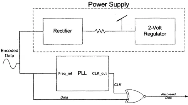
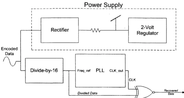
In this chapter I describe the implementation and operation of the basic BPSK re-ceiver, before clock division is applied. The receiver has three main parts: the clock and data recovery (CDR) PLL, the data recovery circuitry (an XOR gate), and the power supply. Figure 3-1 is the block diagram of the circuit. The implementation assumes the properties of the incoming signal that were discussed in Section 1.4. The receiver would work as I describe it here, but it consumes more power than is acceptable in this application.
Power Supply
2-Volt Regulator Encoded L---I Data Freqref PLL CLK out -CLK3.1
Phase Locked Loop
A coherent receiver is necessary to decode PSK signals, since all the information is
encoded in the phase. This is in contrast with FSK or FM signals, in which the information is stored in the frequency, the time derivative of phase. Since absolute phase has no meaning without a reference point, it is naturally easier to decode the derivative of the phase; a coherent receiver does the extra work to set up that starting point. As a result, a coherent receiver typically requires more power.
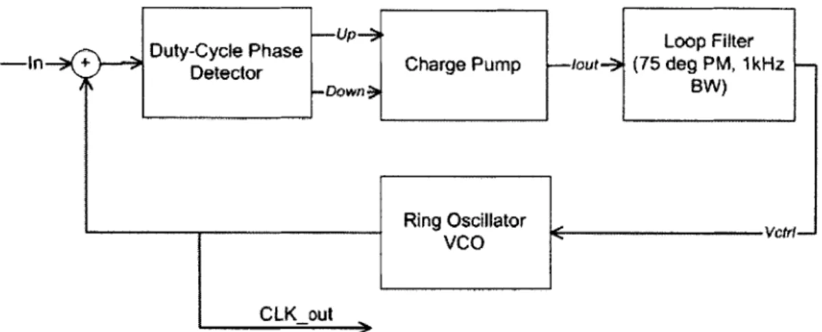
Duty-Cycle Phase-U-) Loop Filter
-in + Dtyctor PsCharge Pump -lout-- (75 deg PM, 1 kHz
--Down- BW)
Ring
Oscillatorvctet-VCO CLKout
Figure 3-2: Block Diagram of CDR PLL
I chose to build a CDR PLL to create the coherence. The important difference
between CDR PLLs and other types is that the PLL remains active while data is transmitted, rather than having separate locking and reading phases. The only way that a PLL can continue to operate while reading data is to reject the disturbances that the data creates in the lock. This can be accomplished by setting the loop bandwidth to a lower frequency than most of the data energy. In addition, CDR
PLL's are made with very high phase margin (~ 750), so that any disturbances that
are inside the loop bandwidth settle smoothly. Figure 3-2 is the block diagram of my
PLL.
However, because the data is a simple random sequence with rectangular bits, its power spectral density is a squared sinc function centered at zero. No matter how small the loop bandwidth becomes, there will always be energy present in the data at
a lower frequency. The next section on Manchester Encoding explains how to encode data to minimize its content at low frequencies.
3.1.1
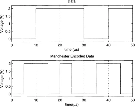
Manchester Encoding
It makes sense to first think of the low frequency energy in the time domain. A random bit sequence can generate an arbitrarily long chain of zeros or ones so that in the limit, the data begins to look like a DC signal. The simplest solution to the problem is Manchester Encoding: a scheme in which a bit is represented by either a falling or rising edge [2]. In other words, a "0" is represented by "01" and a "1" is represented by "10". A sample data sequence is given in Figure 3-3.
Data CO 0 Q) 0) 0 2 1.5 1 0.5 0 2 1.5 1 0.5 0 ) 10 20 30 40 5 time (ps)
Manchester Encoded Data
10 20 time(pts) 30 40 0 0 50
Figure 3-3: A Demonstration of Manchester Encoding. The original data (top) is multiplied by a square wave at frequency equal to the data rate , rd. In the Manchester Encoded data (bottom), a logical "0" is represented by "01" and a "1" is represented
by "10". The dashed lines are the bit boundaries.
-Encoded in this fashion, the lowest frequency data now corresponds to a string of alternating ones and zeros. Here is a depiction:
1 0 1 0 1 -- 10 01 10 01 10
Since each bit in the encoded sequence is half the length of an original bit, the frequency of this sequence looks the same. The slowest frequency of the new waveform is equal to fastest possible frequency in the old.
For frequency domain analysis, this encoding can be seen as multiplying the data sequence by a square wave with frequency at rd. Normally, the power spectrum of the data is a squared sinc function, centered at 0Hz and with nulls at every multiple of
rd/2. Due to the Manchester encoding, this power spectrum is then convolved with the Fourier transform of the encoding square wave, which consists of delta functions
at odd multiplies of Td. The resulting spectrum has its main lobes at ±rd and a null
at 0. The low frequency components of the data are thus eliminated, allowing the PLL to reject the disturbances due to the data.
3.1.2
Duty Cycle Phase Detector
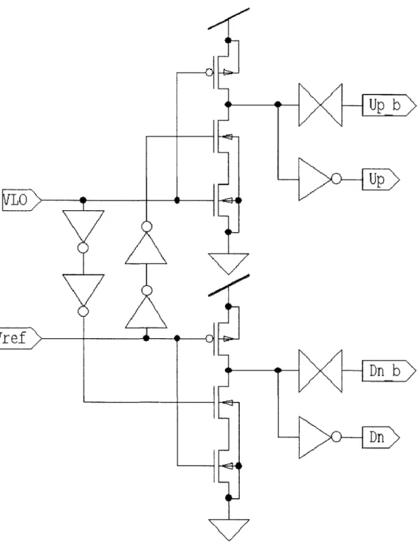
The phase detector I used in this project was originally designed by a classmate of mine, Colin Weltin-Wu, for a class project. I call it the "Duty Cycle Phase Detector"
(DCPD) because it operates with 50% duty cycle outputs in lock. This design is
more robust than many standard sequential phase detectors that turn the charge pump completely off in lock. Since the system is not ideal, the edges of the reference and local oscillator do not appear exactly simultaneously, even in lock.
In the standard detectors, such as the Ti-State Phase-Frequency Detector [4], when an edge of either the local oscillator or the reference comes, one of the control signals, either Up or Down, immediately turn on. The signal is then reset when the other edge comes. However, due to injection in the charge pump, a small, fixed amount of current will escape the pump for however short a time it is turned on. The net effect is a spike of current which can look the same for several values of the phase
difference near lock, or more simply, a dead zone. 0.- 04 > 0.6 > 0.3 - -02 0.2 .2
0~0-~-02
-056-0 -0,8 -014-2pi -3p./2 -p. -0//2 0 pi/2 Pi 3pL/2 2p -p. -3 4 -p./2 -p14 0 pi/4 p./2 3 U4 p.
Phase Differe..c Phase Differeme
(a) Tri-State Phase-Frequency Detector (b) Duty Cycle Phase Detector
Figure 3-4: Nonlinear Phase Characteristics of Two Phase Detectors (Dead Zones Exaggerated for Illustration)
This nonlinearity will exist whenever the charge pump turns on only momentarily. However, in the DCPD, that same nonlinearity occurs when the signals are 1800 out of phase, and thus it is not critical. Instead, there is a smooth line through zero phase. The two different phase detector characteristics, including the non-linearities,
are given in Figure 3-4.
The DCPD is presented in Figure 3-5. It generates its control signals in the following manner: When both the local oscillator, VLO, and the PLL input, Vref, are high, both Up and Down transition high. Next, when the detector encounters a falling edge of the local oscillator, Up goes low, and when the reference generates a falling edge, Down transitions low. These last two events are independent of the order in which they happen. By turning both signals on at the same time, the system guarantees that the output that is active longer corresponds exactly to the input that falls second. Thus if that local oscillator is high longer, then the frequency is too slow, and Up is held longer than Down. One side effect of this detector is decreased range in detection, since it only has half the cycle to work with. This effect is reflected in Figure 3-4(b), in the decreased maximum output and range. The gain, however, is unchanged.
LOUp
Figure 3-5: Duty Cycle Phase Detector. The local oscillator and reference inputs are compared and the outputs, Up and Down are sent through equal delays.
3.1.3
Charge Pump
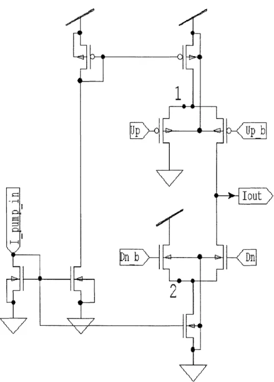
Because the DCPD causes the charge pump to burn current half the time, even in lock, it is very crucial that the up and down currents be matched and charge injection be limited, in order to avoid phase error. After several iterations, the charge pump design I used focuses on minimizing charge injection with a differential current scheme. Figure 3-6 provides the circuit diagram.
The two branches of the pump merely move the currents around, rather than shutting them off entirely. The charging current switches between charging the filter capacitor and draining to ground. The same is true of the discharging current and the power supply. This way, the voltage at the sources of the switches (Nodes 1 and 2 in Figure 3-6) remain at a nearly constant voltage, reducing charge injection from the switches. With a single ended circuit, each time the current turns off, charge is deposited on the parasitic capacitance of the switch, due to the changing voltage across it. In a differential scheme, the switch source voltage remains nearly constant, as does the output voltage of the filter capacitor, so there is virtually no charge to deposit.
An added benefit of the differential scheme is that cascode transistors come for free. When the switch is off, it acts as a cascode transistor, increasing output resistance and reducing early effect. The cascodes are not ideal because the cascode bias is all the way at the rails, but the effect is still present. It should be possible to switch between a cascode bias and fully on, rather than between the rails, but the implementation has other complications and proved unnecessary for the accuracy required.
The final aspect of this charge pump is that all the transistors are large in order to reduce threshold mismatch during fabrication.
3.1.4
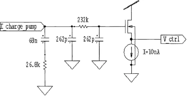
Loop Filter and VCO
The loop filter is the part of the circuit that makes it a CDR PLL. I implemented
a third order passive loop filter with 750 of phase margin and a loop bandwidth of
n
b\-2
1
I
Dn
Figure 3-6: Differential Charge Pump. Redirects charging and discharging currents between the two branches. Top and bottom half are independent. Nodes 1 and 2 stay nearly constant due to the differential nature of the circuit. Iout connects to the loop filter charging capacitor.
$Z::
4
a zero to counteract the pole created by the change from phase to frequency present
in all PLLs. The 1kHz bandwidth is a factor of 100 slower than rd, ensuring that the
loop will be unaffected by the data. The structure of the filter and component values
I chose are given in Figure 3-7.
-232k
I
Charge
pump
V
68n
-262p
262
p
V ctrl:)
I=1nA
26. Ok
Figure 3-7: Third order loop filter designed by Lee's "cookbook" method. All poles except one are beyond crossover.
In his textbook, Tom Lee gives a "cookbook formula" for creating third order loop
filters with the right parameters
(4].
I used his method to create the basic loop filter.I added a level shifter after the filter, which is necessary for correct DC voltages. It acts as a very high frequency pole that, for the purposes of this filter, can be ignored. The VCO that provides the eventual clock is also a standard circuit. I used a current-starved ring oscillator, controlled by a transconductance amplifier. The gain
of the VCO is about 50 M7.
3.1.5
PLL performance
The PLL performance was only tested after clock division at 27MHz/16 and is de-scribed in Chapter 4.
3.2
Power Supply and Data Recovery
The rest of the receiver's implementation is less critical to the central project, but I discuss it here for completeness.
3.2.1
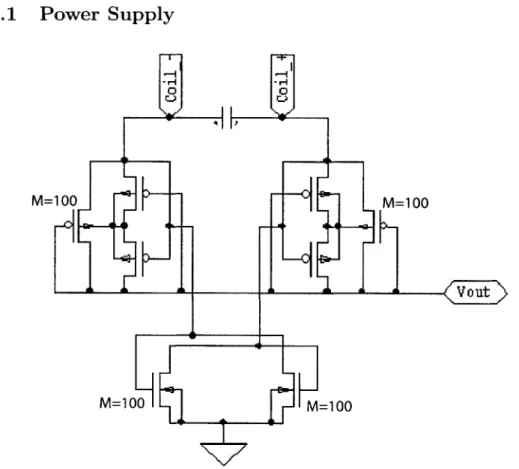
Power Supply
I
-0 0
M=1M00 M=100
M=100 M=100
Figure 3-8: Ghovanloo and Najafi's rectifier. The extra PMOS transistors set the well potential to the highest point. This reduces the gain of parasitic bipolars, and thus
reduces latchup [31. The measure M is the equivalent transistor width, with M=1
being one 12 x 6 transistor.
The power supply is one of the reasons that this system fits the constraints of much higher transmission frequency than data rate. It consists of a MOS rectifier and a
2V regulator to supply VDD. I borrowed the rectifier design from Maysam Ghovanloo
and Khalil Najafi [3], and it is presented in Figure 3-8. The paper has an interesting trick to avoid latch-up by keeping the p-well at the highest available potential. The rectifier will also include a band-pass filter, tuned to 27.12MHz, at the front end. The
tuning capacitor is part of the rectifier, and the inductor will be built on a testing board. The inputs Coil+ and Coil- are the two ends of the inductor. The filter will
have as high a Q as possible, but not greater than 4, due to the resistance in the coil.
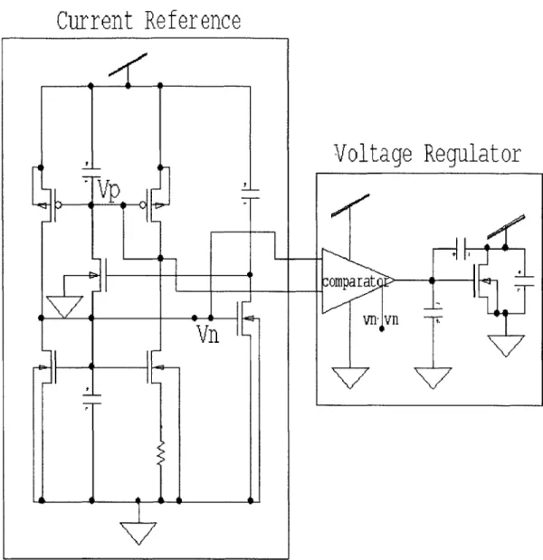
Node Vout feeds into the voltage regulator to set VDD. The voltage regulator uses a
current reference to set the gate-to-source voltage of an N-FET, and through sizing and a Widlar mirror, uses the same current to set a P-FET's gate-to-source voltage.
Finally, a comparator turns on a pull-down transistor connected to VDD until the two
gate-to-source voltages voltages add to VDD. The resistor and FETs are sized so that
Vn = .8V, VP = 1.2V, and VDD = 2V. The circuit diagram is included in Figure 3-9.
Thanks to Soumyajit Mandal for the design.
3.2.2
Data Recovery
All that is needed in the data recovery is an XOR gate. I also added a register to
clean up the data, since a small amount of phase error causes the XOR gate to pulse. This works because the data is only coded to one bit per symbol. Comparing with the clock, the data is either identical or inverted, the definition of BPSK (see Figure
3-10). If the data were to shift by some fraction of 7r, such as in quadrature PSK,
where jumps of 7r/2 indicate data, more work would needed to detect it, and perhaps a faster clock. This smaller shift is one pitfall of clock division, and is discussed in depth in Chapter 4.
Current Reference
-4- AVp.
I
Voltage Regulator
omparat
I
vn- vn
Figure 3-9: 2V Voltage Regulator. The current reference sets Vn and sets
VDD = V, + VP. The voltage regulator portion turns the shunt transistor on if
Vn - VP. This in turns burns more current through VDD, changing V, and
com-pleting the feedback loop. The capacitors in the current reference are for startup and filtering, and the capacitors in the regulator are for compensation.
d
-_L
P
_QRecovered Clock (from PLL)
BPSK Encoded Data
Recovered Data = Encoded Data @ Clock
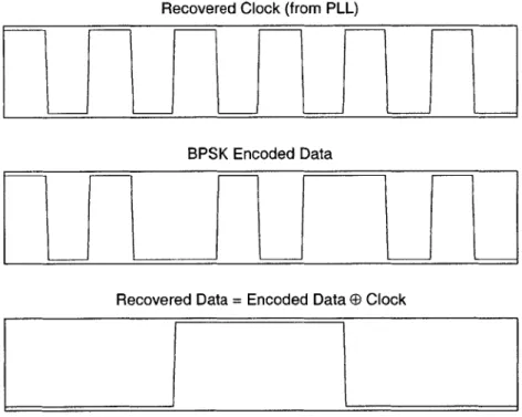
Figure 3-10: An XOR gate decodes BPSK data by comparing the clock (top) and a encoded signal (middle). The resulting waveform (bottom) is exactly the data.
Chapter 4
Clock Division and Its
Consequences
Clock division is a very simple physical technique with some very interesting results. It involves running the received input signal through a counter with value N, where N
is the frequency divide ratio. For 201 < N < 2', this is a a-bit counter. Figure 4-1
is a new block diagram of the receiver with the clock divider included. The result is an input to the PLL with frequency fo/N. The only strict constraint on values of
N is that f0
/N
> rd. However, often several clock cycles will be needed for robustdata detection, so N should not usually approach that limit. In the cochlear implant
system, N = 16 (a = 4) and fo/rd = 271.2, so there are about 17 clock cycles per
data bit.
The first consequence of clock division is the predicted one: it reduces power. Since the PLL never sees any signal but the divided one, it behaves as if the signal
were transmitted at f0
/N.
Thus, in my system, the PLL locks at about 1.7MHz, orfo/16, just as if a 1.7MHz signal were transmitted through the air. It is obvious that due to slower switching in the ring oscillator, a slower PLL will use less power. The exact relationship between power and frequency becomes important when a system
approaches the limit of fo/rd, which this system does not. That is because until that
limit is approached, the bit error rate remains close to constant, while the power consumption is reduced consistently with increasing N. The power consumed by
Power Supply
Rectifier A2Vl
Regulator
Encoded
L.---Data
Divide-by-16 Freq ref PLL CLK, out
Divided Data Rtare
Figure 4-1: BPSK Receiver Block Diagram. The clock divider has been added. This is the complete block diagram.
the 1.7MHz PLL is 5.8pW and the clock divider consumes an overhead of 7.8pW. Together, this is a factor of 10 improvement over the estimate of 135pW in the faster
PLL.
The overhead cost of the divider is important in order to evaluate the value of clock division. Because the divider is a digital circuit that switches constantly, the
power cost of each piece is given by CTOTVADf, where f is the switching frequency.
For the LSB of the counter,
f
= fo, and for the next,f
=fo/
2, and so on. The
total power is the sum of each. Thus the divider power is a linear function of fo and a logarithmic power of N. For a given fo, then, as the limits of clock division are approached, the power consumption of the divider increases in order log N, while the PLL power decreases in order N. Therefore, clock division is still viable for increasing
N.
A second, qualitative effect of clock division is that a slower PLL will lock more
easily given a fixed bandwidth. Since rd is fixed, the bandwidth of the PLL cannot
increase, or the PLL will try to lock to the data. Thus as fo increases, the bandwidth becomes a smaller fraction of fo. In addition, the VCO gain increases with fo, making
the PLL more sensitive to changes on the control line, Vctrl. All this makes the system less stable, and makes it more difficult to retain a lock.
4.1
Detection Difficulties
4.1.1
Short Pulse Output
There are inherent complications associated with applying clock division to a PSK signal. As an example, take BPSK data modulated on a pure sine wave carrier of
radial frequency wo, where wo = 27rfo. Let us also assume, for the sake of simplicity,
that the signal has zero initial phase. There is no loss of generality in using this assumption, since absolute phase is unmeasurable. The transmitted form of a "0" is in this case
A cos(wot),
while a "1" is represented by
A cos(wot t 7r).
When the input is passed through the clock divider, the entire argument of the cosine is divided by N so that the waveforms look as follows:
0 - A cos = A cos (t) (4.1)
1 -+ A cos N A cos -t t (4.2)
Because the divider is a digital counter, it also acts as a limiter so the wave is no longer a cosine, but rather a cosine with all the odd harmonics added in. However, the argument is unchanged by that fact. As relation 4.2 shows, the new divided data
has a ir/N shift, rather than a a full shift of 7r (an inversion), as originally expected.
The ir/N shift is depicted in Figure 4-2. With a full shift of tr, the waveforms would
be inverted. Instead, the data waveform lags only by 7r/N in phase.
0"1" to arw by a1 f t b o r 0 >0 oi T
the smaller detectable pulse width. In addition, because the pulses are so narrow,
jitter
in the PLL becomes much more important: I = only 11.25 of phase, and the thejitter
can be as much as 10. Phase noise of the data itself is not a significant problem because the system requires a signal with large enough amplitude to power it. This automatically makes the SNR large enough for the noise in the data to be overwhelmed by the jitter in the PLL.4.1.2
More Than One Possible Output
If the output or the XOR appeared as either zero phase or a short pulse, it would be a small matter to design a detector for it. However, that is not the case. In fact, there are many different possible pulse lengths as outputs. To understand the reason for this, it is important to first discuss one important aspect of the data encoding
in the transmitter. In the previous section I discussed the form of the data bits in
BPSK. In doing so, I stated that a "1" is represented by a phase shift of tr. We'll
see shortly why this is the case.
Normally, to encode one data bit, the intuitive idea would be to add 7r to the
carrier phase, advancing the signal. And then to return to zero phase, the encoder would delay the carrier. This makes sense; it would cause the data to be represented
by phases of zero and 7r, or zero and 7r/N when divided. However, the physical
encoding of the signal is not done with advances and delays in phase. Instead, since a full shift in BPSK is the same as multiplying the carrier by -1, the encoding actually
multiplies the carrier by 1 and -1 to encode "O"s and "1"s, respectively. Thus any
data transition is encoded by changing the sign of the carrier.
The net effect here is that every time an inversion of the data comes it creates an extra edge in the carrier. This is what is supposed to happen; the carrier immediately
flips sign. Note that these transitions are asynchronous with the carrier, since foird
is not an integer. In effect, this advances the data every time, since the next rising edge, and thus the next flip flop trigger comes earlier. Figure 4-3 is a depiction of the arrival of two data bits. For the purposes of illustration, the data rate in the figure is
much closer to the carrier frequency than it is in reality. In addition, N = 4 in this
figure.
As I mentioned briefly earlier, the carrier is actually a sine wave. However, for the purposes of the following discussion, let us assume that the it has already been limited as it will be in the divider. Figure 4-3 first shows the raw carrier inside the transmitter, along with the modulated carrier. The next two waveforms are the modulated waveform after the first flip flop, clock divided by two, and then, after a second flip flop, divided by four. The clock division occurs with each toggle flip flop triggering on the rising edges of the previous waveform. This illustrates why adding
Carrier
Modulated
Carrier (MC)/
DMder
Input
__-MC
(Divided
by 2)
MC
(Divided
by
49
Carrier
(Divided
by
4)
XORout
Figure 4-3: Accumulation of Divided Phase. Several waveforms are presented to illustrate how divided phase is accumulated on each data transition. These waveforms depict an N = 4 case, with two data transitions at the arrows. The data and carrier are then divided and the XOR output is the phase difference. XOR-out shows that by switching data twice, the phase difference
Another important point illustrated in the figure is that it does not matter whether the inversion causes a rising or falling edge in the modulated carrier, even though the detector only triggers on rising edges. This is because if a rising edge is created, the latches immediately respond, and if a falling edge is created, the following rising edge occurs where there would have been a falling edge before. Either way, the net effect is a rising edge that appears earlier than it would have if no data transition occurred. In Figure 4-3, the first edge created is a rising edge, yet the second is a falling edge. Both have the same result of accumulating phase. This can most clearly be seen in the XOR output, which increases pulse width by 7r/N = 7r/4 for every transition.
So now we understand that the phase actually advances on every data transition, and thus as the bits change, the phase cycles through all its possible values. But this is still a relatively well-behaved system, with a few more complications than predicted. As long as the phase predictably accumulates, a detector can be created to decode the data.
However, in simulation I discovered that the phase does not always accumulate, but rather it sometimes decreases, too. As I mentioned earlier in this chapter, the
Limiting
threshold
Data edge
Figure 4-4: The limiting threshold in the divider is uneven. As a result, inversions do not always add an edge, but sometimes remove them. The sine wave does not cross
the threshold due to the inversion, and as a result, the limited signal is delayed rather than advanced.
limited by the first flip flop in the divider. This is significant because the flip flop is not ideal, and the limiting threshold is not exactly halfway between the rails. In
Figure 4-4, I show how a threshold that is 75% of VDD can cause an edge to be skipped
rather than added. If the data transition had not come, the sine wave would have crossed the threshold much earlier than it did. As a result, the limited signal loses an edge and is delayed, rather than advanced as it should be.
Since the phase can move in either direction, the system is not as predictable as it might be, and we need a solution to phase dividing that prevents this from happening. In the next section I explain why the phase moving in both directions can end up in system malfunction, with the PLL losing lock.
4.2
Phase Transitions and the Random Walk
Since there is a certain probability of adding or subtracting phase on any given tran-sition, the data output, or more correctly, the phase difference, is able to wander. Specifically, it behaves as a one-dimensional, simple random walk, where the phase difference On is defined as
i=0
where xi E {-1, 1}, with probability p and 1 - p respectively, and n is the number of
data transitions that have occurred.
The random walk implies that
#4
has a binomial distribution on [-, ] at allmultiples of 7r/16 (See [1] for a further discussion of binomial distributions).
Since phase is periodic in 21r and 27r is a multiple of 7r/16,
#,
has a finite numberof states, as if constrained on a circle. What this means is that for very large n,
#
becomes uniformly distributed on the interval [-7, 6] (see Appendix A for theproof). So after enough time has passed, the phase is just as likely to be in any of its
32 possible states.
Since a binomial distribution is memoryless, the distribution looks the same
could be any one of 32. So at a given time, the likelihood is for the phase to stay close to its current state, which could be any of them.
The problem with this it that the PLL could potentially be caught in a state where the phase difference is something other than zero for a significant amount of time. As a result, the PLL could try to lock to a new value of the phase, causing data errors. This can be easily seen in Figure 4-2. If the clock in the bottom graph moves even 7r/16 due to a change in the lock, then the data and clock will be perfectly aligned, and the data "1" will be read as a "0".
In Section 3.1.1, I cited an analogous problem as the reason for Manchester
Encod-ing. In that case, a long string of "1"s can be represented as 0, = ir for an indefinite
time, which we wanted to avoid. Again, the reason was that the PLL would try to
lock to the new value of the phase,
#,
= 7r, causing data errors. The main differencenow is that we have N times less tolerance for phase error, because the data pulses are that much shorter.
In light of the problems that come with phase division, a solution is needed that will provide clock division for power reduction, but will not divide the phase-encoded data. In the next chapter, I discuss "N-7r Shift Encoding", which does exactly that.
Chapter 5
N-T Shift Encoding
In order to recover the proper signal after clock division, the system must counter the
phase division associated with it. Since it is not possible to do this in the receiver
without significantly changing the hardware, the solution is to encode the transmitted waveform differently to account for the problem. The original data should be encoded such that after phase division the data transitions consist of advancing or delaying the carrier by exactly one half period, or adding or subtracting exactly 7r from the phase. Since the receiver divides by a factor of N, a data transition must be encoded
by a shift of N7r in phase. I have called this encoding scheme "N-7r Shift Encoding".
In this chapter I discuss first what it means to subtract Nir from a signal. I then provide a simple implementation that can be added to the back end of a typical BPSK transmitter. Next, I perform a frequency analysis of the new waveform in order to determine that transmission through a narrow channel is reasonable. This frequency analysis is important because the scheme relies on digital encoding, which can result in a great deal of spectral waste. In this system, however, simple filtering can reduce the waste to decent levels while preserving the data in the signal. Finally, I will suggest a few possibilities for future work to expand this project to more complex data transmission systems.
IH
(a) Typical transition: adding an edge and thus adding 7r
i
I(b) Thresholded transition: skipping an edge and subtracting 7r
Figure 5-1: Demonstration of the phase counting model of edge detection. The change in data (thick dashed line) causes either an addition or subtraction of 7r by adding or subtracting edges compared to the clock (not shown). The expected falling edge is marked by the thin dashed line.
5.1
Adding N-r To the Phase
Before entering into the discussion of N-qr Shift Encoding, it is important to under-stand one major difference between this encoding scheme and most others. Whereas most encoding schemes modify the data before modulating it onto a particular carrier, it is necessary in this scheme to modify the carrier directly. This is the main reason
that the frequency analysis in Section 5.3 becomes necessary - there is no longer a
pure carrier modulating data, so the newly encoded data could very well have a large bandwidth.
The need for carrier modification is directly due to the need to delay by more than one full period. In a sine wave, there is no way to do this, since it looks the same after every period. This holds for any periodic input to a detector that counts phase directly, in an analog sense. An example of this would be a mixer, which has an immediate output directly corresponding to the phase difference. However, the divider does not count phase directly, but rather only samples phase at each edge. It is this distinction that allows the system to subtract more than 27r from the input.
The model of phase that an edge detector employs is that every edge marks the passing of one half period and w in phase.
This model works when compared with what the original BPSK signal was doing: the data would change in the middle of a clock cycle, causing the an extra edge to appear, resulting in inversion. This is illustrated in Figure 5-1(a). Figure 5-1(b) is the an example of the thresholded signal, where the inversion delays the carrier, removing an edge. The thick dashed line is the data transition and the thin line is where the next edge would have come if not for the data. Both methods work in this case, since
adding and subtracting 7r amount to the same thing, as I discussed in Section 4.2.
Using this model, it's easy to see that if a data transition causes the signal to skip
N edges, Nir of phase will be subtracted, which is exactly what we want. In order
to add Nir to the phase, N extra edges would have to be inserted in a single clock cycle. The generation of these extra edges would require a clock at fo, which is what the system is trying to avoid. So for practical purposes, N-ir Shift Encoding only
subtracts N7r for each data transition, no matter what the absolute value of the data is. Absolute "O"s and "1"s will be determined by convention before data is sent.
When the signal is clock divided, N = 7r will be subtracted from the phase.
Figure 5-2 is a demonstration of this for N = 16, which is the case for my example
system. The top graph shows a downward data transition that causes the encoded waveform to skip 16 edges, or 8 full clock cycles. The same happens with rising edge transitions. 0U CU 0, Idatetooter 4.5 4. 4.? 4.8 4.0 5. 5.2 5S4 6. 58 57 Ths. W4 .....4 . 4.6 4.A 4. 4.9 4.0 5D- 6.1
Figure 5-2: On the data transition (top), the encoded signal or 8 full cycles.
(bottom) skips 16 edges,
It is interesting to note that an analog frequency divider, such as a subharmonic mixer, would still encounter both the phase division and random walk. This is because these effects are only dependent on when the data changes relative to the carrier, phase can either be added or subtracted from a sine wave exactly the same as in a square wave (See relation 4.2). However, there would be no simple solution to these problems because it is impossible to add more than 27r to a sine wave. Thus we were lucky that the system uses a digital divider, allowing this scheme to work.
5.2
Simple Digital Implementation
In constructing a circuit to implement this scheme, I started with only two signals: a 27.12MHz clock and the data. The key to this solution is that the new waveform is merely a Boolean addition of the clock with a signal that rises on any data edge and lasts N/2 full cycles (two edges per clock cycle). A block diagram of this solution is included in Figure 5-3, and the circuit schematic itself is given in Figure 5-4. The initial state of all toggle-configured flip flops is low. In the following discussion of how the encoder works, refer to Figure 5-5, which gives samples of each of the internal waveforms discussed.
First, I needed to be able to detect an edge of the data, and since it's unimportant which kind of edge passes, the detector consists only of a register and an XOR gate. The register delays the incoming signal by one clock cycle, and then the XOR gate compares the two signals. If the data changed, the XOR gate will output a pulse of exactly one clock cycle on Data-Pulse.
This signal, which I call DataPulse in the diagram, has two functions. First, it acts as a start bit for the a-bit counter. (Recall from Chapter 4 that N = 2c.) The second function is to act as the start bit for the register which outputs Long-Pulse.
The a-bit counter counts to N, and with an a-input AND gate, stops itself. The same internal signal used to reset the counter is then output to the LongPulse generating flip-flop.
The boolean addition of DataPulse and the counter output create DbLPulse, which as the name suggests, consists of two pulses. These two pulses toggle the flip-flip, so that it outputs a pulse that lasts N/2 total cycles. It lasts N/2 cycles, as opposed to N, because the LSB in the counter is the clock itself.
Finally, Long-Pulse and the clock are input to an OR gate, and the result is the encoded output, Waveform.
There is a small amount of circuitry not included in the block diagram. The first of those extra pieces is another register, used to clean up the signal, since the final OR gate could potentially have glitches. The rest of the extra circuits are startup
Figure 5-3: Block Diagram of N-ir Shift Encoder Edge Detector Data D " D 0 Pulse - DbI Pulse CLK Full Il-bt Counter DbI 2gPt
s Long Pulse Waveform
LongPulse b
Figure 5-4: N-7r Shift Encoder. Takes data in and outputs the digital waveform with
N edges skipped. Needs to be filtered before transmission.
Da ta tas
DaEdge
D
Q-Dete~tr DblPulse CLKDeetrjb DataPulse LongPulse IN,
Str
bit
271Mz L outrend WaveforrmWaveform