HAL Id: hal-02289565
https://hal.archives-ouvertes.fr/hal-02289565
Submitted on 16 Sep 2019
HAL is a multi-disciplinary open access
archive for the deposit and dissemination of
sci-entific research documents, whether they are
pub-L’archive ouverte pluridisciplinaire HAL, est
destinée au dépôt et à la diffusion de documents
scientifiques de niveau recherche, publiés ou non,
electrostatics induced by a nanometer-thick molecular
underlayer
Ather Mahmood, Cheol-Soo Yang, Seunghun Jang, Lucie Routaboul, Hyunju
Chang, Alessio Ghisolfi, Pierre Braunstein, Laetitia Bernard, Tindara
Verduci, Jean-François Dayen, et al.
To cite this version:
Ather Mahmood, Cheol-Soo Yang, Seunghun Jang, Lucie Routaboul, Hyunju Chang, et al.. Tuning
graphene transistors through ad hoc electrostatics induced by a nanometer-thick molecular underlayer.
Nanoscale, Royal Society of Chemistry, 2019, �10.1039/C9NR06407A�. �hal-02289565�
rsc.li/nanoscale
Nanoscale
rsc.li/nanoscale
ISSN 2040-3372
PAPER Shuping Xu, Chongyang Liang et al. Organelle-targeting surface-enhanced Raman scattering (SERS) nanosensors for subcellular pH sensing
Volume 10 Number 4 28 January 2018 Pages 1549-2172
Nanoscale
This is an Accepted Manuscript, which has been through the
Royal Society of Chemistry peer review process and has been
accepted for publication.
Accepted Manuscripts are published online shortly after acceptance,
before technical editing, formatting and proof reading. Using this free
service, authors can make their results available to the community, in
citable form, before we publish the edited article. We will replace this
Accepted Manuscript with the edited and formatted Advance Article as
soon as it is available.
You can find more information about Accepted Manuscripts in the
Information for Authors
.
Please note that technical editing may introduce minor changes to the
text and/or graphics, which may alter content. The journal’s standard
Terms & Conditions
and the
Ethical guidelines
still apply. In no event
shall the Royal Society of Chemistry be held responsible for any errors
or omissions in this Accepted Manuscript or any consequences arising
from the use of any information it contains.
Accepted Manuscript
View Article Online
View Journal
This article can be cited before page numbers have been issued, to do this please use: A. Mahmood, C. Yang, S. Jang, L. Routaboul, H. Chang, A. Ghisolfi, P. Braunstein, L. Bernard, T. Verduci, J. Dayen, P. Samorì, J. Lee and B. Doudin, Nanoscale, 2019, DOI: 10.1039/C9NR06407A.
Journal Name
ARTICLE
Received 00th January 20xx, Accepted 00th January 20xx DOI: 10.1039/x0xx00000x www.rsc.org/Tuning graphene transistors through ad hoc electrostatics induced
by a nanometer-thick molecular underlayer
Ather Mahmood
a†
,
Cheol-Soo Yang
b†
,
Seunghun Jang
b†
,
Lucie Routaboul
c,
Hyunju Chang
b,
Alessio Ghisolfi
d, Pierre Braunstein
d, Laetitia Bernard
e, Tindara Verduci
a, Jean-François Dayen
a,
Paolo Samori
f, Jeong-O Lee
band Bernard Doudin
aWe report on the modulation of the electrical properties of graphene-based transistors that mirrors the properties of a few nanometers thick layer made of dipolar molecules sandwiched in-between the 2D material and the SiO2 dielectric substrate.
The chemical composition of the films of quinonomonoimines zwitterions molecules adsorbed onto SiO2 has been explored
by means of X-ray photoemission and mass spectroscopies. Graphene-based devices are then fabricated by transferring the 2D material onto the molecular film, followed by the top source-drain electrodes deposition. The degree of supramolecular order in disordered films of dipolar molecules was found to be partially improved as a result of the electric field at low temperatures, as revealed by the emergence of hysteresis in the transfer curves of the transistors. The use of molecules from the same family and suitably designed to interact with the dielectric surface yields a disapperance of the hysteresis. DFT calculations confirm that the dressing of the molecules by an external electric field exhibits multiple energy minima landscape that explains the thermally-stabilized capacitive coupling observed. This study demonstrates that the design and exploitation of ad-hoc molecules as interlayer between a dielectic substrate and graphene represents a powerful tool for tuning the electrical properties of the 2D material. Conversely, graphene can be used as an indicator of the stability of molecular layers, by providing insight into the energetics of ordering of dipolar molecules under the effect of electrical gating.
Introduction
In the last decade graphene has emerged as an exciting new material displaying exclusive optical, electrical, thermal and mechanical properties, with potential impact on many realms of science and technology.1 Among numerous outstanding
characteristics, its highest surface-to-volume ratio makes it extremely sensitive to environmental changes at the nanoscale. The unique electrostatic sensitivity of graphene to nearby molecules is key since it allows to tune the properties of the 2D material for applications in hybrid molecules-graphene based devices.2 It is indeed notorious that the operation and
performance of graphene-based solar cells,3 organic electronics4
and chemical/gas sensors 5,6 critically depend on the interface
between the surface of the electrically conducting 2D material and the (conjugated) organic molecular layers. The vast majority of studies7 reported so far have focused on the interactions between
graphene flakes supported on a solid substrate and molecules adsorbed on its top in the form of single-molecules,8 self-organized
thin films9,10 or supramolecular architectures.11 By fabricating
planar FET devices, the graphene-substrate electrostatic interactions can possibly impact the transistor properties, with the nearby charges locally doping the graphene layer and shifting the neutrality point. Such electrostatic influence of adsorbed molecules on top of graphene is well-documented.12,13
However, what lies underneath graphene also matters. Recent findings revealed that graphene can be ‘chemically transparent’ since the chemical environment underneath its surface affects the properties of the material grown on its top.14 Nevertheless, studies
on the inverse FET geometry, based on graphene lying on top of a molecular layer, are much scarcer. To our knowledge, they are limited to functionalized substrates for charge screening purposes, aiming at improving the performance of the transistors by shifting their electrostatically-induced doping (or related work function)
15,16,17 or to ferroelectric molecular layers designed for driving a
very large graphene doping.18
We propose to exploit graphene as a tool to explore the properties of an underlying molecular film grown on a dielectric substrate. It
a.University of Strasbourg, CNRS, IPCMS UMR 7504, 23 rue du Loess, 67034,
Strasbourg, France.
b.Korea Research Institute of Chemical Technology (KRICT), 19 Sinseongno,
Yuseong-gu, Daejeon 305-600, Korea.
c.LCC-CNRS, Université de Toulouse, CNRS, UPR 8241, 205 route de Narbonne,
31077 Toulouse Cedex 4.
d.University of Strasbourg, CNRS, CHIMIE UMR 7177, Laboratoire de Chimie de
Coordination, 4 rue Blaise Pascal, 67081 Strasbourg, France.
e.Swiss Federal Laboratories fo Materials Science and Technology (EMPA),
Überland Strasse 129, 8600 Dübendorf, Switzerland
f.University of Strasbourg, CNRS, ISIS UMR 7006, 8 allée Gaspard Monge, F-67000,
Strasbourg, France.
† Equal contributors
Electronic Supplementary Information (ESI) available: [details of any supplementary information available should be included here]. See DOI: 10.1039/x0xx00000x
Nanoscale
Accepted
Manuscript
Published on 05 September 2019. Downloaded on 9/13/2019 7:30:30 AM.
View Article Online
ARTICLE
Journal Name
2 | J. Name., 2012, 00, 1-3 This journal is © The Royal Society of Chemistry 20xx
Please do not adjust margins
Please do not adjust margins
is also fair to note that the characterization of molecular layers adsorbed onto dielectric surfaces is experimentally much more challenging then when conducting substrates are exploited. This is because surface imaging or spectroscopy tools, including scanning tunneling microcopy, (ultraviolet)photoemission or inverse photoemission spectroscopies, require substrates stables under electric charging.
Here, we investigate ultra-thin films of overall neutral yet dipolar molecules, which can be expected to influence the electronic properties of graphene, bypassing the complications related to the presence of counter-ions associated with charged species. We take advantage of our previous endeavor on the synthesis of a family of zwitterion molecules, their assembly from solution into ultra-thin films, and the study of their physical and chemical properties when adsorbed onto conductive substrates.19,20,21
Quinonemonoimines zwitterions (QZW, Scheme 1) are characterized by positive and negative charges on opposite sides of the six-membered ring that are electronically decoupled but chemically connected through carbon-carbon single bonds.22,23,24 The overall 12π electrons are partitioned
in two 6π-electrons sub-units, with the positive charge delocalized between the nitrogen functions over four bonds involving 6π-electrons, while the negative charge is likewise spread between the oxygen atoms. This results in a remarkably large electric dipole of typically 10 D across the short planar six-membered ring structure of the benzoquinonemonoimine “core”.23 We previously detailed
how these molecules are prone to undergo spontaneous self-assembly into molecular layer onto gold substrates and show unique electronic properties, making them of interest for enhanced metal-organic interfaces of relevance for organic electronics applications.25 Chemical modification of the
nitrogen-bound end groups represents a facile strategy for the tuning of their reactivity, packing and electronic properties when adsorbed on metals.19,20,26
These dipolar molecules are therefore particularly suited to be interfaced with a graphene surface via electrostatic interactions. The specific choice of the molecular design, which takes full advantage of our developed knowledge, is tailored in order to meet the following characteristics:
1 is our best documented member of the family, which
has been previously shown to assemble into compact nm-thick films over metallic surfaces. 19,20,26
2 showed better affinity for Au than SiO2, as revealed by
XPS mapping over patterned Au on SiO2,20 and is
therefore expected to have small interactions with the
SiO2 substrate.
3 is expected to interact with SiO2 substrate, forming a
QZW layer featuring a greater stability than 1 or 2. The molecular films have been investigated by combining X-ray photoelectron spectroscopy (XPS) and time of flight secondary ion mass spectroscopy (ToF-SIMS) analyses. While the former offers insight into the chemical composition of the adsorbed molecules, the latter provides information on the thickness, quality and integrity of ultra-thin molecular films supported on SiO2
substrates. The electrical characteristics of graphene FET devices built over thin molecular films adsorbed onto such dielectric substrates are exploited as internal gauge to evaluate the stability of such molecular layer, thus using graphene as ‘detector’ of the underlaying film.
Experimental
Devices construction
General procedure for the synthesis of the zwitterions.
Commercial 4,6-diaminoresorcinol dihydrochloride and functional amines were used directly without further purification. Solvents were freshly distilled under argon prior to being use. 1H NMR
spectra were recorded in CDCl3 on a Bruker 500 MHz instrument,
operating at 125 MHz for 13C spectra and 500 MHz for 1H spectra.
Chemical shifts are given in units, in parts per million (ppm) relative to the singlet at = 7.26 for CHCl3. The splittings were
designated as s, singlet; d, doublet; t, triplet; m, multiplet; br, broad. Zwitterions 1 and 2 were readily prepared following published procedures.27,20
The synthesis of (6Z)-4-(3-(methoxydimethylsilyl)propan-1-
amino)-6-(3-(methoxydimethylsilyl)propan-1-iminio)-3-oxocyclohexa-1,4-dien-1-olate (3) was performed from a suspension of the parent zwitterion 1 (0.100 g, 0.72 mmol) in freshly distilled methanol (10 mL) to which 3-(ethoxydimethylsilyl)propylamine (0.290 mL, 1.52 mmol) was added. The solution was heated under argon at 100 °C for 3 h (preheated oil bath). After cooling to room temperature, the reaction mixture was filtered and the solid collected was extracted with ethanol. The solution was concentrated under reduced pressure and addition of diethyl ether precipitated the zwitterion as a violet-pink solid which was washed successively with ether and pentane (0.147 g, 51%). 1H NMR (500 MHz, CDCl3): 0.12 (s, 12H, Si-CH3), 0.65 (m, 4H, Si-CH2), 1.77 (m, 4H, N-CH2-CH2), 3.36 (m, 4H, N-CH2), 3.41 (s, 6H, Si-OCH3), 5.14 (s, 1H, N···C···CH), 5.43 (s, 1H, O···C···CH), 8.28 (br s, 2H, NH). 13C1H NMR (125 MHz, CDCl3): -2.68 (s, Si-CH3), 13.40 (s, Si-CH2), 22.42 (s, N-CH2-CH2), 45.92 (s, N-CH2), 50.47 (s, Si-OCH3), 80.68 (s, N···C···CH), 98.92 (s, O···C···CH), 156.67 (s, N···C), 172.43 (s, O···C).
Graphene fabrication. Graphene was grown using low-pressure
chemical vapor deposition (LPCVD) methods on a Cu foil (Alfa Aesar, Item No. 46986, 99.8%, cut into 6 cm strips) in a hot wall furnace consisting of a 4 in. fused silica tube. Prior to CVD, the foils were cleaned using a Ni etchant (Transene, TFB) for 5 min and then
Scheme 1. Chemical structure of molecules 1, 2 and 3.
Page 2 of 9
Nanoscale
Nanoscale
Accepted
Manuscript
Published on 05 September 2019. Downloaded on 9/13/2019 7:30:30 AM.
View Article Online
Journal Name
ARTICLE
rinsed with DI water 3 times. A typical growth process flow is as follows: (1) load the Cu foil, evacuate, heat to 1000 °C, and annealing for 20 min under a 100 sccm H2 flow (at a pressure of
about 70–80 mTorr); (2) introduction of 30 sccm CH4 and 30 sccm
H2 for 40 min (60 mTorr); (3) cooling down the furnace to room
temperature in vacuum, after exposure to CH4 for 40 min. A PMMA
solution (950 K, 4% by volume dissolved in chlorobenzene) was spin-coated onto the top of the sample at 2000 rpm for 30 s. The PMMA film (thickness of 200 nm) was then dried at 30 °C overnight. The Cu under the graphene film was etched using a copper etchant solution and washed with deionized water 3 times. The resulting PMMA/graphene layer was collected and transferred on a SiO2 substrate functionalized with QZW molecules. Finally, the
PMMA film was dissolved using acetone. Graphene etching is achieved by Ar ion bombardments that are accelerated at 400 V from the initial gas introduced with a flow rate of 3 sccm at a pressure of 10-4 mbar. In contrast, Ar ion etching, being more
directed and less diffusive, resulted into functional patterned devices.
Molecular films growth. 10 mM solutions of dichloromethane
solution of molecules 1-3 were processed at surfaces following two methods. In method 1, the SiO2/Si substrate was rinsed with
dichloromethane. The molecular film was prepared by spin-coating: a drop the QZW solution was applied onto the basal plane of the surface, then the sample was spun at 2000 rpm for 30 s. This process was repeated 3 times. In method 2, the SiO2 substrate was
cleaned with dichloromethane and immersed in the QZW solution for about 18 h in a sealed container. When the substrate was taken out, dichloromethane quickly evaporated and an uneven layer of zwitterion molecules was observed by optical microscopy. The functionalized substrate was then rinsed with a highly diluted QZW solution (conc = 0.5~1 mM) in dichloromethane to remove the excess zwitterion molecules, and then washed by sample spinning at 500 rpm for 10 s followed by 3000 rpm 30 s. This process was repeated twice. XPS analysis of the films of molecules 1, 2 prepared using the two different methods gave similar results. Atomic force microscopy imaging revealed covered substrates of limited roughness. More specifically, while the pristine SiO2
substrates revealed a root-mean square roughness (RRMS) of 0.15
nm as determined on areas of 2 x 2 m2 , upon absorption of the
molecular layer the RRMS was found being below 1 nm for
molecules 1,2 and below 2 nm for molecules 3.
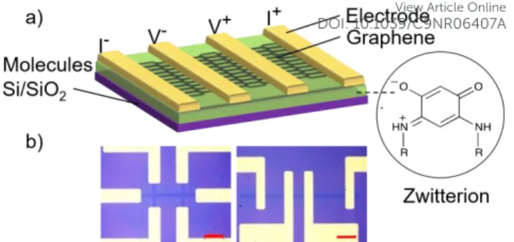
Graphene transistors fabrication. The chosen graphene
transistors architecture comprises a bottom-gate, based on Si-n++
substrate covered by a 300 nm thick thermally grown SiO2 layer,
and top source/drain Au electrodes, 30 nm thick, evaporated though a shadow mask yielding channels lengths of several hundreds of m and channel widths of 40 m (Figure 1 a,b). For the purpose of investigating how the buried molecular underlayer impacts graphene transistor properties, it is of paramount importance to avoid heating and solvent processing when transferring the graphene layer. We therefore employed a recently
developed solvent-free approach.28 To cross-check the quality of
the transferred CVD graphene, we used Raman spectroscopy which revealed that our transistors comprise uniform graphene (mostly bilayer) and exhibit good electrical properties (mobility > 1000 cm2V-1s-1, clean quantum hall plateau at low
temperatures).28
Surface spectroscopy characterization. In order to reveal and
quantify the presence of thin molecular films adsorbed onto SiO2,
two complementary methods were used. XPS Measurements were performed by using the Thermoscientific K-Alpha XPS system (Al Kα 1486.6 eV). All data were calibrated to a C-C bond energy of 284.9 eV. The beam spot size was focused to 400 μm2 at the
take-off angle of 90°. A pass energy of 20 eV was implemented and energy step size of 0.05 eV was used. The acquisition time was set to 200 ms and 10 scans of data were recorded, with measurements performed on two regions of the sample. All measurements were conducted at pressures < 6×10⁻⁸ Torr. XPS spectra were recorded
on samples prior and after the deposition of the graphene films.
ToF-SIMS measurements were performed with an instrument
from IONTOF GmbH, Germany. Mass spectra were acquired using 25 keV Bi3+ primary ions in high mass resolution mode (~5000)
under the static limit (< 1012 ions/cm2). Positive secondary ions in
the mass range 1–800u were recorded on randomly selected areas of 200 x 200 µm2. To ensure reproducibility of the results, two
measurements were performed on each sample and compared. Cross-check measurements with same operating parameters were carried out on pure bulk molecules (compressed powder) and on bare silicon substrates.
Results and discussion
Figure 1. Design of the samples a): Schematics of the
graphene-over-molecules device; b): Optical micrograph of typical devices investigated (scale bar is 200 m long).
Nanoscale
Accepted
Manuscript
Published on 05 September 2019. Downloaded on 9/13/2019 7:30:30 AM.
View Article Online
ARTICLE
Journal Name
4 | J. Name., 2012, 00, 1-3 This journal is © The Royal Society of Chemistry 20xx
Please do not adjust margins
Please do not adjust margins
We first took great care to ensure and quantify the presence of compact molecular thin films on the dielectric substrate. Figure 2 shows XPS spectra measured from all three molecules deposited on SiO2 substrate. In contrast to bare SiO2 and graphene/ SiO2
substrates exempt of detectable XPS signal of N, we observed that deposition of 1-3 on SiO2 resulted in detectable N1s peak, which
cannot be attributed to the solvent (Figure 2a). Successive rinsing with ethanol (up to 5 times with 10 s immersion in solvent) did not noticeably modify the XPS N peak, providing unambiguous evidence for the stability of the molecular films. Importantly, no noticeable difference in the N1s spectra were found on sample prior or after graphene deposition.
The Si2p background peak was also recorded for 1-3 on SiO2 and
compared to the data on as-prepared initial SiO2 substrate (Figure
2b). As expected, the Si2p peak at 103.5 eV decreases when substrates are coated with the QZW films of molecules 1 and 2, with a further decrease for 3, also showing additional spectroscopic features, corresponding to the energy of bulk Si atoms, likely to result from those of molecule 3.
From the literature XPS absorption of self-assembled monolayer, revealing an extinction length of 4 nm,29 we estimate that
molecules 1,2 form layers thinner than 1 nm, while molecules 3 make thicker films, around 4 nm in thickness.
Further insight into the presence of the molecules of interest on the support was gained by the use of ToF-SIMS that offers both elemental and molecular information of surfaces with ppm sensitivity. Hence, it enables to detect full molecular species of molecules 1, 2 and 3 on SiO2, demonstrating their presence and
integrity on surfaces. Figure 3 (top) shows part of the positive spectrum recorded on a molecular film of 3. Four characteristic peaks can be observed in the mass region of the full molecule. The
far-left peak, at mass 399u, corresponds to the full molecule plus one hydrogen ([M+H]+). This confirms the presence of the
molecule 3 on the substrate. Additionally, one can see another peak at mass 385u and a dominant peak at mass 371u. These correspond to the molecule 3 after the loss of one and both methyl termination(s) respectively. Remarkably, this confirms that the molecule 3 spontaneously releases the methyl groups to form Si-O-Si bonds with the substrate. Further, the relative intensities of these three peaks demonstrate that the latter binding scheme is the dominant one.
The bottom part of Figure 3 displays zoom-ins on the main molecular ion ([M+H]+) of the molecules 1 (a), 2 (b) and 3 (c). The
results for SAM samples (red traces), bulk molecules (dashed blue traces) and substrate reference (black traces) are presented and compared. In all three cases, the peak is found to be characteristic (large intensity from the bulk molecule and no intensity from the substrate reference) and demonstrates the presence and integrity of the molecule on the SiO2 substrate. Note that due to different
ionization potential of different molecular species and the large dependence of matrix effect, the respective intensities cannot be compared nor estimated from the bulk situation.
Overall, the combination of XPS and ToF-SIMS confirms the presence of uniform films with thicknesses below 5 nm, covering the surface of the SiO2 substrate for molecules 1-3, with good
confidence that the molecules remain intact after deposition, and a device construction methodology that ensures that the graphene “lid” on the top did not perturb significantly these assemblies.
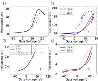
Top-contacts bottom-gate graphene transistors supported on SiO2 showed strongly p-doped characteristics, with significant
hysteresis in the transfer curves, even though the gate voltage was slowly swept (90 mV/s, Figure 4). Hysteresis and
Figure 2. a): XPS N1s spectra of molecules 1, 2, 3 (black, red
and blue), respectively over SiO2 substrates. Data shown after
the graphene over-layer transfer are identical to those prior to addition of graphene; b): XPS Si 2p spectra of molecules 1,
2, 3, respectively over SiO2 with the same color notation as
left figure. The data in green color is taken on bare SiO2
substrate.
Figure 3. Top: ToF-SIMS positive mass spectrum of molecule 3
adsorbed on SiO2, in the region of molecule 3 atomic mass
([M]). Target molecule with and without its methyl terminations and byproduct are observed. Bottom: ToF-SIMS positive mass spectra of molecules 1 a), 2 b) and 3 without the methyl terminations c), adsorbed on SiO2 (red), as compared
to the references spectra of bare SiO2 (black) and bulk
respective molecules (dashed blue).
Page 4 of 9
Nanoscale
Nanoscale
Accepted
Manuscript
Published on 05 September 2019. Downloaded on 9/13/2019 7:30:30 AM.
View Article Online
Journal Name
ARTICLE
neutral point shift can be reduced by vacuum annealing treatment (down to 10-4 mbar, with the samples kept at 200
°C), a procedure previously shown to enhance significantly the quality of the transistors.28 Here, we avoided this
procedure by preventing heating in order to guarantee the integrity of the adsorbed molecules. We previously showed that CVD graphene devices of high quality can be obtained by proper substrate and post-treatment procedures,28 and we
traded off here the FET properties for better confidence in the chemical integrity and reproducibility of our devices. The observed deviations from ideal behavior relate to trapped molecules (solvent, oxygen, moisture) and electric-field-induced defect in the dielectrics that shift the local density of states of the graphene layer. The so-called positive hysteresis properties of the transfer curves, that shift the neutrality point to more positive gate voltage when sweeping back from large positive bias, persist in vacuum down to 1.5 K on samples with graphene transferred on bare SiO2 substrates
(Figure 4a). This observed hysteresis is commonly attributed to charge trapping in the substrate that imprints local changes in the graphene density of states.30,31 For applied gate voltage
below 70 V, no hysteresis was observed in the temperature range 300 - 1.5 K for the long measurement time scale used.
The capacitive coupling between graphene and nearby charges yields a negative hysteresis behavior: when sweeping back from high positive voltages, the neutrality point is displaced to more negative voltage values.30 Such negative hysteresis is usually
explained as resulting from (partial) freezing of the alignment of dipolar molecules in the immediate neighborhood of the active graphene layer under the electric field created by the gate voltage. This is for example observed for ion-gated graphene devices.32
Dipolar molecular adsorbates, in particular oxygen and moisture,
can also induce negative hysteresis. This is well-known with interstitial water,33 the hysteresis strongly diminishing below 0 °C,
where the electric susceptibility of frozen water becomes negligible.
In our experiments, transistors comprising inter-layers of molecules 1 and 2 display the appearance of negative hysteresis (Figure 4 b, c). However, this occurs only if the temperature is low enough (a few K), under rather low gate voltage bias (several tens of V). Such hysteresis becomes negligible for temperatures greater than 10 K when a slow gate voltage sweep rate was used. A slow relaxation of the resistance correlates with the observed hysteresis (Figure 5). An exponential slow relaxation of the sample resistance is revealed in the lowest temperature range, with a time constant of typically 102-104 s (depending on the temperature and
the history of the sample), while absent at higher temperature, where the hysteresis disappears.
One must emphasize that the temperature trend of the negative hysteresis is opposite to the one previously reported in literature.32,33 Clearly, the transition temperatures cannot
correspond to freezing or a phase transition of (unlikely) solvent residues. Furthermore, negative hysteresis does not occur for the test molecule 3, which was designed to strongly bind to the SiO2
substrate. Indeed, transistors including molecules 3 exhibit a small positive hysteresis under larger voltage stress (Figure 4d), which resembles the behavior found on devices without molecules, even though the presence of molecules 3 on the substrate is validated by ToF-SIMS and XPS. In essence, low temperatures negative hysteresis unambiguously relates to dipolar QZW molecules weakly bound to the substrate.
Figure 4. Transistor transfer curves of CVD graphene transferred
on SiO2 devices. a): sample transferred over bare SiO2, measured
at room temperature, nearly temperature-invariant; b) c) d):devices with substrates covered by QZW molecular layers made of molecules 1, 2, 3 prior to graphene transfer. Hysteresis of the transfer curve is roughly temperature–independent and small for bare SiO2 and requires a larger gating bias to appear.
Very large hysteresis occurs at lower temperatures for molecules
1, 2, while absent at higher temperatures under moderate gate
bias. In contrast, hysteresis similar to bare SiO2 case occurs for
molecule 3.
Figure 5. Time evolution of the graphene layer resistance over
molecules 1, after a 0 - 40 V voltage step. The resistance at 1.5 K varies exponentially, with a fitted time constant of 264 s.
Nanoscale
Accepted
Manuscript
Published on 05 September 2019. Downloaded on 9/13/2019 7:30:30 AM.
View Article Online
ARTICLE
Journal Name
6 | J. Name., 2012, 00, 1-3 This journal is © The Royal Society of Chemistry 20xx
Please do not adjust margins
Please do not adjust margins
Quantitative insight into the energetic of QZW molecules (molecule 1) on SiO2, under applied electric field, was gained by
calculations using the Nudged Elastic Band method (NEB).34 We
simplified our model system to the maximum level, to extract the key points explaining the experimental findings. The atomic geometries of all the model structures were calculated by using the Vienna ab initio simulation package.35,36 The exchange–
correlation functional was approximated using the Perdew– Burke–Ernzerhof expression.37 In particular, the optB86b-vdW
functional, implemented in VASP by Klimeš et al. to account for weak van der Waals (vdW) interactions, was used to calculate the optimized structures.38 Electron–ion interactions were modelled
using the projector-augmented wave method.39
The electronic wave functions were expanded in a basis set of plane waves with a kinetic energy cut-off of 400 eV.
To compute the initial and final structures needed to perform the NEB calculation, we prepared the reconstructed (001) alpha-quartz surface as the SiO2 surface structure.40 Geometry relaxation
step in NEB calculation was repeated until the ionic forces were reduced to values below 0.1 eV/Å. The k-space Brillouin-zone integrations were carried out using only the gamma-point. For all the SiO2 surfaces, the middle SiO2 monolayer was fixed during
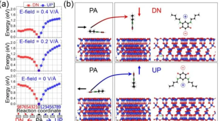
structure optimization. In all models studied using this calculation, at least 20 Å-thick vacuum regions along the perpendicular direction (z) to the two-dimensional slab were included to minimize interactions between neighbouring image cells. Figure 6 shows the energy profiles (a) and atomic geometries (b) upon rotating the QZW molecule on SiO2 from a parallel (face-on)
configuration (‘PA’), with molecule lying flat on the substrate, to an orientation normal to the substrate with its dipole pointing upwards (configuration ‘UP’), or pointing downwards (configuration ‘DN’). Non-interacting QZW molecules on SiO2
prefer to lay flat on the substrate, in agreement with previous
scanning probe imaging studies performed on low coverage films.41,21 Yet, intramolecular interactions in tightly packed layers
formed by solution processing can exhibit a different behavior,20
and it is clear that the adsorption potential energy minimum at low angle values (between molecule and substrate) cannot be applied to our experimental situation. Data of Figure 6 results from energy calculations under an applied electric field of 0, 0.2, and 0.4 V/Å respectively, for positive gate bias, estimated to correspond to the largest applied fields in the experiments shown in Figure 5. To maximize the electrostatic interactions, the negative pole of the
molecules prefers to point towards to positively biased substrate, explaining the lower energy values when the molecules point downwards.
We propose here that the observed negative hysteresis is due to a difference of the constrained orientation (or ‘dressing’) of the molecules under electric field. At negligible applied gate voltage (state O in Fig. 7), the energy configurations for the two rotations
PA➝DN and PA➝UP are degenerate. When increasing the gate
voltage (state B in Fig. 7), PA➝DN is energetically more favorable, and a tendency to dress the molecules downwards emerges. At higher gate bias (state C in Fig. 7), a stable energy minimum develops for a large angle of the molecules, which can be considered energetically stable in the DN configuration, with an
Figure 6. a): Nudged elastic band energy profiles; b): atomic
geometries of the rotations of QZW molecule 1 on SiO2, under
given applied electric field of 0, 0.2 and 0.4 V/Å, for the paths from parallel configuration (PA) to 1st perpendicular configuration, where the molecule dipole points down (DN), and from PA to the other perpendicular configuration with dipole pointing up (UP). The red, blue, black, green, and white balls represent O, Si, C, N, and H atoms, respectively.
Figure 7. Evolution of dipole population due to the rotation of the
QZW molecular on SiO2 under applied electric field. Sweeping the
gate voltage relates to the sequence O➝ B➝ C➝ B’. In state
O, the energy profiles are symmetrical (in Fig. 6) for the two
directions of molecules rotations, under the hypothesis of a zero electric field. When increasing the electric field value, the DN orientation is energetically preferred (state B). Upon further increase of the gate voltage makes the DN orientation at nearly -90o a (meta) stable local minimum of energy. The related reverse
energy barrier makes the high angle dressed molecules freeze when sweeping back the gate voltage (state B’). Estimates of the populations of molecules in DN and UP configurations are included in the figure. This makes the populations of B different from those of B’, the latter having a memory of the populations reached in C.
Page 6 of 9
Nanoscale
Nanoscale
Accepted
Manuscript
Published on 05 September 2019. Downloaded on 9/13/2019 7:30:30 AM.
View Article Online
Journal Name
ARTICLE
energy barrier E limiting their probability to escape. This stable statistical occurrence of a population of dipoles pointing down can persist when sweeping back the gate bias voltage, and makes the statistical distribution of the molecules orientations in the state B’ differ from the previous state B. The energy barrier E therefore creates a difference of the conductance state, between B and B’, related to the memory of the dressing in the DN configuration that occurred at the highest gate voltage applied.
Since the energy barrier E is small, being estimated in our calculations as low as ∼0.1 eV, it is only at the lowest temperature range that the ‘reverse’ transition path DN➝PA becomes thermally impeded, and the related hysteresis develops. At 25 K, this property disappears, being nullified by the thermally driven motion of the molecules. One can even distinguish a slight overshoot of the resistance value, correlated with the small positive hysteresis observed at 25 K in Fig 5. Such thermodynamic ‘viscosity’ is well known in the field of (nano)magnetism, where a complicated multi-minima energy landscape describes equilibrium magnetic configurations.42 Here, we simplified our
model to emphasize the two minima energy landscape that explains our findings
.
Conclusions
In summary, our study shows how the electrical read out in graphene-based transistors is a unique tool to gain detailed insight into insulating molecular films deposited over a dielectric substrate. We illustrate this concept on ultrathin films of quinonoid zwitterion molecules 1-3 intercalated between the SiO2
dielectric substrates and the graphene active layer. The transfer curves recorded at the lowest temperatures (< 25K) reveal that the dipolar alignment of the molecules under gating electric field can be stabilized, for molecules 1,2 making ultra-thin layers with no indications of strong interactions with the substrate.
Temperature represents also a powerful remote control to modify the electrostatic effect of the molecular film on the device operation: when the temperature exceeds a few tens of K the thermal motions smears out the role played by the presence of the molecules on the transistor device output. However, low temperatures make possible molecular ordering stabilization under electric field, revealed by the graphene ‘detector’. Here, the emergence of hysteresis in the transistor transfer curve indicates that such dipolar films made of quinonoid zwitterions can exhibit hysteresis in their polarizability, in analogy to ferroelectrics. Deeper insight into the energetics of the system is needed to clarify if this is a single molecule property or a collective effect, as well as better quantify how graphene plays an active stabilizing role.
Our data details unprecedented temperature dependence properties of graphene transistors; it therefore contributes to better pinpoint the origin of hysteresis in graphene FETs, being a key technological issue requiring better clarifications in the community. It also demonstrates that graphene can be
used as an electrical ‘detector’ of molecular thermal motions, with a potential for dynamics insight in a very wide frequency range. Finally, the construction of molecular layers-graphene hybrid systems made it possible to monitor the emergence of novel properties of molecular systems, which are highly relevant for applications in the field of information storage using multi-functional or multiferroic materials.
Conflicts of interest
There are no conflicts to declare.
Acknowledgements
This work was supported by the Agence Nationale de la Recherche (FUNGRAPH 11-IS10-003 02, Labex NIE 11-LABX-0058_NIE within the Investissement d’Avenir program ANR-10-IDEX-0002-02), the International Center for Frontier Research in Chemistry (icFRC), the NRF-ANR program through the National Research Foundation of Korea funded by the Ministry of Education, Science and Technology (NRF_2011-K2A1A5-2011-0031552), and the European Commission through the Graphene Flagship Core 2 project (GA-785219). The technical support of the STnano cleanroom is also gratefully acknowledged, especially H. Majjad help for AFM imaging.
Contributions
J. L., C.Y. and B.D. conceived the experiment, performed by C.Y. and A. M. with S.J. handling the calculations and modeling. L.R., A.G. and P.B synthesized the molecules, H. C. helped for the CVD and J.D. for the transport measurements. L.B., T.V. and P.S. performed the surface spectroscopy studies. All authors contributed to the manuscript writing.
Notes and references
1 A. C. Ferrari, F. Bonaccorso, V. Fal’ko, K. S. Novoselov, S. Roche, P. Bøggild, S. Borini, F. H. L. Koppens, V. Palermo, N. Pugno, J. A. Garrido, R. Sordan, A. Bianco, L. Ballerini, M. Prato, E. Lidorikis, J. Kivioja, C. Marinelli, T. Ryhänen, A. Morpurgo, J. N. Coleman, V. Nicolosi, L. Colombo, A. Fert, M. Garcia-Hernandez, A. Bachtold, G. F. Schneider, F. Guinea, C. Dekker, M. Barbone, Z. Sun, C. Galiotis, A. N. Grigorenko, G. Konstantatos, A. Kis, M. Katsnelson, L. Vandersypen, A. Loiseau, V. Morandi, D. Neumaier, E. Treossi, V. Pellegrini, M. Polini, A. Tredicucci, G. M. Williams, B. Hee Hong, J.-H. Ahn, J. Min Kim, H. Zirath, B. J. van Wees, H. van der Zant, L. Occhipinti, A. Di Matteo, I. A. Kinloch, T. Seyller, E. Quesnel, X. Feng, K. Teo, N. Rupesinghe, P. Hakonen, S. R. T. Neil, Q. Tannock, T. Löfwander and J. Kinaret, Nanoscale, 2015, 7, 4598– 4810.
2 K. S. Novoselov, A. K. Geim, S. V Morozov, D. Jiang, Y. Zhang, S. V Dubonos, I. V Grigorieva and A. A. Firsov,
Nanoscale
Accepted
Manuscript
Published on 05 September 2019. Downloaded on 9/13/2019 7:30:30 AM.
View Article Online
ARTICLE
Journal Name
8 | J. Name., 2012, 00, 1-3 This journal is © The Royal Society of Chemistry 20xx
Please do not adjust margins
Please do not adjust margins
Science (80-. )., 2004, 306, 666–669.
3 H. Wang, Y. Liu, M. Li, H. Huang, H. M. Xu, R. J. Hong and H. Shen, Optoelectron. Adv. Mater. Rapid Commun., 2010, 4, 1166–1169.
4 S. Pang, Y. Hernandez, X. Feng and K. Müllen, Adv.
Mater., 2011, 23, 2779–2795.
5 W. Yuan and G. Shi, J. Mater. Chem. A, 2013, 1, 10078. 6 C. Anichini, W. Czepa, D. Pakulski, A. Aliprandi, A.
Ciesielski and P. Samorì, Chem. Soc. Rev., 2018, 47, 4860–4908.
7 M. Gobbi, E. Orgiu and P. Samorì, Adv. Mater., 2018, 30, 1706103.
8 F. Schedin, A. Geim, S. Morozov, E. Hill, P. Blake, M. Katsnelson and K. Novoselov, Nat. Mater., 2007, 6, 652– 655.
9 L. Newton, T. Slater, N. Clark and A. Vijayaraghavan, J.
Mater. Chem. C, 2013, 1, 376–393.
10 N. N. Nguyen, S. B. Jo, S. K. Lee, D. H. Sin, B. Kang, H. H. Kim, H. Lee and K. Cho, Nano Lett., 2015, 15, 2474–2484. 11 M. Gobbi, S. Bonacchi, J. X. Lian, Y. Liu, X.-Y. Wang, M.-A. Stoeckel, M. A. Squillaci, G. D’Avino, A. Narita, K. Müllen, X. Feng, Y. Olivier, D. Beljonne, P. Samorì and E. Orgiu,
Nat. Commun., 2017, 8, 14767.
12 X. Wang, J.-B. Xu, W. Xie and J. Du, J. Phys. Chem. C, 2011, 115, 7596–7602.
13 A. Matković, M. Kratzer, B. Kaufmann, J. Vujin, R. Gajić and C. Teichert, Sci. Rep., 2017, 7, 9544.
14 S. Chae, S. Jang, W. J. Choi, Y. S. Kim, H. Chang, T. Il Lee and J.-O. Lee, Nano Lett., 2017, 17, 1711–1718. 15 W. H. Lee, J. Park, Y. Kim, K. S. Kim, B. H. Hong and K.
Cho, Adv. Mater., 2011, 23, 3460–3464.
16 K. Yokota, K. Takai and T. Enoki, Nano Lett., 2011, 11, 3669–3675.
17 N. Cernetic, D. O. Hutchins, H. Ma and A. K.-Y. Jen, Appl.
Phys. Lett., 2015, 106, 021603.
18 Y. Zheng, G.-X. Ni, C.-T. Toh, M.-G. Zeng, S.-T. Chen, K. Yao and B. Özyilmaz, Appl. Phys. Lett., 2009, 94, 163505. 19 J. Xiao, Z. Zhang, D. Wu, L. Routaboul, P. Braunstein, B.
Doudin, Y. B. Losovyj, O. Kizilkaya, L. G. Rosa, C. N. Borca, A. Gruverman and P. a Dowben, Phys. Chem. Chem.
Phys., 2010, 12, 10329–40.
20 L. Routaboul, P. Braunstein, J. Xiao, Z. Zhang, P. A. Dowben, G. Dalmas, V. Da Costa, O. Félix, G. Decher, L. G. Rosa and B. Doudin, J. Am. Chem. Soc., 2012, 134, 8494–8506.
21 D. A. Kunkel, J. Hooper, S. Simpson, D. P. Miller, L. Routaboul, P. Braunstein, B. Doudin, S. Beniwal, P. Dowben, R. Skomski, E. Zurek and A. Enders, J. Chem.
Phys., 2015, 142, 101921.
22 A. Sawicka, P. Skurski and J. Simons, Chem. Phys. Lett., 2002, 362, 527–533.
23 O. Siri and P. Braunstein, Chem. Commun., 2002, 379, 208–9.
24 Y. Haas and S. Zilberg, J. Am. Chem. Soc., 2004, 126, 8991–8998.
25 Google Patents, WO2012/025878, 2012.
26 L. G. Rosa, J. Velev, Z. Zhang, J. Alvira, O. Vega, G. Diaz, L. Routaboul, P. Braunstein, B. Doudin, Y. B. Losovyj and P. A. Dowben, Phys. Status Solidi Basic Res., 2012, 249, 1571–1576.
27 Q.-Z. Yang, O. Siri, H. Brisset and P. Braunstein,
Tetrahedron Lett., 2006, 47, 5727–5731.
28 A. Mahmood, C. S. Yang, J. F. Dayen, S. Park, M. V. Kamalakar, D. Metten, S. Berciaud, J. O. Lee and B. Doudin, Carbon N. Y., 2015, 86, 256–263.
29 C. D. Bain and G. M. Whitesides, J. Phys. Chem., 1989,
93, 1670–1673.
30 H. Wang, Y. Wu, C. Cong, J. Shang and T. Yu, ACS Nano, 2010, 4, 7221–7228.
31 G. Kalon, Y. Jun Shin, V. Giang Truong, A. Kalitsov and H. Yang, Appl. Phys. Lett., 2011, 99, 2011–2014.
32 A. Veligura, P. J. Zomer, I. J. Vera-Marun, C. Józsa, P. I. Gordiichuk and B. J. Van Wees, J. Appl. Phys., 2011, 110, 113708.
33 M. Sobrino Fernández, F. M. Peeters and M. Neek-Amal,
Phys. Rev. B, 2016, 94, 045436.
34 G. Henkelman, B. P. Uberuaga and H. Jónsson, J. Chem.
Phys., 2000, 113, 9901.
35 G. Kresse and J. Furthmüller, Phys. Rev. B, 1996, 54, 11169–11186.
36 G. Kresse, J. Non. Cryst. Solids, 1995, 192–193, 222–229. 37 J. P. Perdew, K. Burke and M. Ernzerhof, Phys. Rev. Lett.,
1996, 77, 3865–3868.
38 J. Klimeš, D. R. Bowler and A. Michaelides, J. Phys.
Condens. Matter, 2010, 22, 022201.
39 P. E. Blöchl, Phys. Rev. B, 1994, 50, 17953–17979. 40 W. Gao, P. Xiao, G. Henkelman, K. M. Liechti and R.
Huang, J. Phys. D. Appl. Phys., 2014, 47, 255301. 41 D. A. Kunkel, S. Simpson, J. Nitz, G. A. Rojas, E. Zurek, L.
Routaboul, B. Doudin, P. Braunstein, P. A. Dowben and A. Enders, Chem. Commun., 2012, 48, 7143–7145. 42 E. P. Wohlfarth, J. Phys. F Met. Phys., 1984, 14, L155–
L159.
Page 8 of 9
Nanoscale
Nanoscale
Accepted
Manuscript
Published on 05 September 2019. Downloaded on 9/13/2019 7:30:30 AM.
View Article Online
A graphene transistor can reveal ordering of dipolar molecules forming nm-thick underlayer,
stabilized under electric field at low temperatures.
Nanoscale
Accepted
Manuscript
Published on 05 September 2019. Downloaded on 9/13/2019 7:30:30 AM.
View Article Online
![Figure 3. Top: ToF-SIMS positive mass spectrum of molecule 3 adsorbed on SiO 2 , in the region of molecule 3 atomic mass ([M])](https://thumb-eu.123doks.com/thumbv2/123doknet/13689142.432252/6.893.468.833.110.348/figure-positive-spectrum-molecule-adsorbed-region-molecule-atomic.webp)