(6
Development of a CMOS Preamplifier for Single Ended
Magnetoresistive Heads
by Iyad Obeid
Submitted to the Department of Electrical Engineering and Computer Science in Partial Fulfillment of the Requirements for the Degrees of
Bachelor of Science in Electrical Engineering and Computer Science and Master of Engineering in Electrical Engineering and Computer Science
at the Massachusetts Institute of Technology
May 22, 1998
Copyright 01998 Iyad Obeid. All rights reserved
The author hereby grants to M.I.T. permission to reproduce and distribute publicly paper and electronic copies of this thesis
and to grant others the right to do so.
Author
Department of Electrical Engineering and Computer Science May 22, 1998 Certified by
Professor Charles G. Sodini Thesis Supervisor Certified by
I1
Ii
Ken Maggio S mpany Supervisor Accepted by_ MASSACHUSETTS INSTITUT OF TECHNOLOGY Frederic R. Morgenthaler Chairman, Deparenitommittee on Graduate ThesesJUL
141998
LIBRARIES
EngW
Contents
6. 6.1. 6.2. 6. 6. 6. 6.3. 6. 6. 6. 6. 6. 6.4. 6.5. 6. 6. 6. CMOS DesignStage One Design
Stage One Predicted Behavior - Transfer Characteri 2.1. Midband Gain
2.2. Low Frequency Pole 2.3. High Frequency Pole
Stage One Predicted Behavior - Noise Performance 3.1. Primary Noise Contributors
3.2. gm2eff
3.3. gmleff
3.4. Thermal Noise 3.5. Flicker Noise
Verification of Noise Calculations Multiplexer Design 5.1. Method 5.2. Results 5.3. Decoder stic 31 31 34 34 35 36 38 39 40 41 43 43 44 46 46 49 49 1. Introduction
1.1. Organization of this Thesis 1.2. Background
2. Literature Review 2.1. Bipolar Designs 2.2. CMOS Designs 2.3. Current Mode Designs 2.4. Noise Considerations 2.5. Other Constraints 3. Method 3.1. Design 3.2. Optimization 3.3. Noise Measurement 4. Noise Models
5. Existing Bipolar Design 5.1. Schematic
5.2. Functionality of Schematic 5.2.1. DC Bias Points
7. Optimization 50
7.1. Gain and Bandwidth Optimization 50
7.2. FET Noise Optimization 51
7.2.1. Method 53
7.2.2. M1 Noise 53
7.2.3. M2 Noise 56
7.2.4. R2 Noise 61
7.2.5. Noise Optimization Conclusion 62
8. Comparisons and Conclusions 63
List of Figures
Figure 1: Options for placement of MR head 14
Figure 2: Typical input referred noise curve 18
Figure 3: Bipolar small signal noise model 22
Figure 4: FET small signal noise model 22
Figure 5 : Existing bipolar first stage preamplifer 24
Figure 6: Feedback loop block diagram 26
Figure 7: Source of high frequency node 28
Figure 8 : AC model of the high frequency node 28
Figure 9: Bandpass characteristic of the bipolar preamplifier circuit 30
Figure 10: Stage one block diagram 32
Figure 11: Simplified stage one schematic 32
Figure 12: Voltage controlled current source transconductance amplifier 33
Figure 13 : Low frequency pole block diragram 35
Figure 14 : Parasitic capacitances defining the high frequency pole 36
Figure 15: AC model for high frequency pole 37
Figure 16: CMOS reader half-circuit 39
Figure 17: AC equivalent of reader half-circuit 40
Figure 18 : AC Equivalent Circuit for Solving gm2_eff 41
Figure 19: AC Equivalent Model for Computation of gml_eff 42
Figure 20: Predicted Input Referred Noise Curve 44
Figure 21: Multiplexer Architectures 48
Figure 22: Head selector circuit 48
Figure 23 : Noise contributions from M1 and M2 52
Figure 24 : Total Integrated Noise vs. Ml Width 54
Figure 25: Noise Curves for Various Values of W1 55
Figure 26 : Input Noise vs. W2 57
Figure 27 : Noise Curves for Various Values of W2 58
Figure 28: Noise vs. M2 Width 59
Figure 29 : Input Referred Noise for Various Values of R2 62
Figure 30: Klein and Robinson architecture block diagram 66
Development of a CMOS Preamplifier for Single Ended
Magnetoresistive Heads
by Iyad Obeid
Submitted to the
Department of Electrical Engineering and Computer Science
May 22, 1998
In Partial Fulfillment of the Requirements for the Degrees of Bachelor of Science in Electrical Engineering and Computer Science and Master of Engineering in Electrical Engineering and Computer Science
ABSTRACT
A CMOS preamplifier was designed to bias and read a single stripe magneto-resistive hard disk drive head. The CMOS circuit is designed as a first pass at replacing an existing Texas Instruments bipolar technology circuit that performs the same task. The design constraints were to match the operating parameters of the existing bipolar circuit, most important of which was the noise floor. The measured input referred noise level of the designed CMOS preamplifier (measured using an integrated noise technique) was 229V, as compared with that of the existing bipolar circuit, 12.9uV. An alternate architecture was also explored, but was found to have deficient bandwidth.
Thesis Supervisor: Professor Charles Sodini
Title: Professor of Electrical Engineering and Associate Director, Microsystems Technology Laboratory
Company Supervisor: Ken Maggio Title: Manager, Texas Instruments
Acknowledgements
Many people were instrumental in the completion of this thesis. I was most fortunate to work with a group of people at Texas Instruments who never tired of my incessant questions and who never hesitated to give me impromptu lectures on all aspects of hard disk drive design, analog circuit theory, and layout design. Without all of them, there would surely be no thesis.
My first thanks is extended to the Texas Instruments Preamplifier design team, especially my personal mentor of sorts, Paul Emerson. Paul, and the rest of the engineers in the group, especially Ashish Manjrekar, Patrick Teterud, as well as Bryan Bloodworth and Andreja Jezdic of the Read Channel team, took me under their collective wing and taught me well over a semester's worth of material on the fly. They suffered through a never-ending barrage of questions and always found the time to help me work through some difficult equations, design concerns, or CAD mishaps. I would also like to extend a special thank you to Ken Maggio, the Preamplifier team manager, for all of his concern and guidance throughout my stay at Texas Instruments. Jim Hellums must also be recognized for taking time to explain the TI noise models to me in detail. As the resident noise expert at TI, his help was indispensable. Thanks also go to Ben Sheahan (also of the Read Channel team) for an unending supply of good advice, snappy pep talks, and colorful design analogies (it's time to land...).
John Wallberg, who was my roommate throughout my stay at Texas Instruments, also receives thanks for a semester's worth of encouragement and advice. Having just completed his own M.Eng. thesis, John showed me the ropes of MIT thesis writing, and continuously berated me for not starting to write sooner. He was right.
I should also thank Sami Kiriaki and Dr. Edward Esposito for their outstanding support of my academic endeavors at Texas Instruments. Sami is credited with taking a chance on me and giving me my opportunity to pursue thesis research in the Hard Disk Drive group. Dr. Esposito was nothing short of a miracle worker as a liaison between MIT and TI, especially in arranging the financial terms of my stay with Texas Instruments. As my
TI interviewer back in 1995, Dr. Esposito was my ticket into the company, and for that, he has my wholehearted gratitude.
At MIT, I would like to recognize Dr. Charles Sodini who agreed to advise this thesis, and who took the time to read it and guide me through the writing process. I am most grateful for all of his help. I would also like to thank the MIT EECS department administrator Anne Hunter, who led me through the treacherous pathways of MIT red tape and various departmental regulations. She always has time to answer questions and it is my sincere belief that Course VI wouldn't run nearly as smoothly without her tending to the helm.
Finally, I thank my family and my friends for giving me the constant support I needed to get through this project. My friends are far too numerous to name individually, but nevertheless, they are worthy of my undying gratitude for never being too busy to listen me gripe about slow progress and writing woes. To my parents, George and Simone Obeid, and my brother Samer, I offer the largest and most sincere thanks of all. You are now, and have always been, the backbone of my little world. Thank you.
1. Introduction
The goal of this research was to design a CMOS circuit (using one of two different architectures) to perform within the same design parameters as an existing circuit built using bipolar technology. The circuit in question was designed to bias a hard disk drive single stripe magneto-resistive (MR) read head and to sense and amplify the data signal generated by this head. The existing circuitry, currently in production by the TI preamplifier design team in Dallas, TX, uses a bipolar technology to implement a simple feedback loop that forces a constant bias current throughout the MR head, and a current sense mechanism to detect and amplify the input signal. Each of the two new architectures uses CMOS technology, as it is believed that a CMOS read amplifier will be smaller and cheaper to manufacture.
The hard drive preamplifier is a circuit that biases the hard drive read head and amplifies data being read off of this head. Hard drive read heads come in several varieties, each with different characteristics, and thus each requiring a different preamplifier. At Texas Instruments, pre-amps are designed for magneto resistive heads. An MR head can be thought of as a variable resistor. The head typically has a 'resting' resistance of RMR = 300. During the read mode, this head resistance changes slightly in time as the MR head, mounted on the drive actuator arm, passes through regions of different magnetization. This is a result of the device physics of the head, a topic beyond the scope of this paper. The deviations in head resistance in response to areas of different magnetization are the pre-amp circuit's input signal. The preamplifier detects and amplifies this signal and passes it on to the read channel, where the signal is digitized, processed, and interpreted as a binary data bit-stream.
There are several known methods of establishing the pre-amp read circuit, all of which are implemented on the market today in bipolar technology. As CMOS processes improve however, industry researchers have been moving forwards with development of a purely CMOS reader which, if developed, could be mass-produced cheaper than an equivalent bipolar reader. The primary goal of this research was thus to investigate the
development of a CMOS read preamplifier. Two different architectures were considered for the CMOS design. The first such architecture is the same as the bipolar architecture with CMOS components simply swapped in for the bipolar ones. The second proposed CMOS architecture is taken from a paper written by Klein and Robinson [1]. In their paper, Klein and Robinson propose a more complex architecture for the CMOS reader but argue that the added complexities pay off in terms of system performance.
1.1.
Organization of this Thesis
For my research, I have prepared a complete analysis of the existing bipolar circuit, as well as a CMOS design for accomplishing the same task. Each is evaluated in terms of the relevant system parameters, namely bandwidth, gain, and most importantly, noise. Since bipolar technology is inherently quieter than CMOS, meeting the system noise requirements is the most technically challenging design aspect.
Section 3 describes the methods of this thesis. In particular, the method of circuit design is discussed, as well as the measurement standard developed for quantifying circuit noise measured in SPICE simulations. Section 4 explains the formulas and physics behind some of the more useful noise equations that are applicable to the read amplifier circuitry.
In Section 5 of this thesis, I will present an analysis of the existing TI bipolar architecture, including circuit simulations predicting performance parameters, as well as circuit equations that verify the simulated results.
In Section 6, I will present a parallel analysis of the TI architecture CMOS design. This will also include circuit simulations and hand calculations to verify the simulated results. An explanation of the functional differences in circuit behavior will also be explained. Section 7 will show the optimization process taken to improve the noise behavior in the CMOS design. The alternate architecture design, which was found to be insufficiently fast to serve as a hard disk drive preamplifier, will be presented briefly in the Appendix.
Finally, in Section 8, the CMOS and bipolar designs will be compared, and recommendations will be made regarding the feasibility of the design of a CMOS preamplifier. The ultimate purpose is to present a clear, factual comparison between the designs in order for the production staff at TI to determine the practicality of pursuing a CMOS pre-amp reader.
1.2.
Background
The hard drive preamplifier is typically a dual function IC. While part of the chip is responsible for writing an analog signal onto the magnetic hard drive platters, the other part is responsible for reading the magnetically stored data and preprocessing it for the read channel IC. The scope of this research extends solely to the reader functions of the preamplifier.
The preamplifier reader is typically divided into three stages. The first stage is responsible for biasing the read element (in this case, the MR head) and providing a small amount of signal gain. The second stage provides a high-speed signal gain, while the third stage provides some signal gain as well as some subtle error detection such as thermal asperity detection. The second and third stages are also beyond the scope of this study. Because they consist solely of high-speed differential amplifiers, these stages do not set the fundamental system bandwidth. Furthermore, because of the large gain in each of these stages (A, = 50 ), noise generated there referred all the way back to the first stage input will be divided by the large gain and will thus be relatively negligible. Therefore, it is the first stage that sets most of the preamplifier performance characteristics and thus requires the most analysis.
The goal of the CMOS design is to build the CMOS first stage to meet the system characteristics of the bipolar first stage. These system parameters, as will be shown later, are:
Parameter Target
Bandwidth (low) 176 kHz Bandwidth (high) 300 MHz
Noise 12.91iV*
2. Literature Review
Many designs for preamplifiers (both CMOS and bipolar) have been published recently in various industry publications. These preamplifiers are designed for a variety of applications, ranging from audiocassette playback to measurements in particle colliders. Each of these specialized applications places a unique set of constraints on the amplifier design. Most of these designs however are set to operate at conditions unsuitable for hard disk drive applications.
2.1.
Bipolar Designs
Several interesting designs in bipolar technology suggest ideas that may be exploited in the development of a low noise CMOS preamp for a magnetoresistive drive head. Monti et al present a design for a low noise tape preamplifier in which a single ended input is fed into a differential pair that is self biased with a feedback loop. The loop is externally compensated with an RC pair [2]. The concept of the self-biased closed loop architecture suggests high stability and will be exploited in the CMOS preamp design. In their design of a CMOS preamplifier for capacitative sensors, Stefanelli et al use PMOS devices as the system input (for high input impedance), but then insist on using bipolar technology for the gain stage [3]. They argue that the higher transconductance of bipolar transistors coupled with their extremely low 1/f noise make them superior to CMOS devices for gain purposes. Overcoming the sub optimal transconductance properties of CMOS will be a repeated problem in this research. These two preamplifier designs are fundamentally inadequate as a guide for the design of an MR head preamplifier however, as they are not required to bias the read element in any fashion. Biasing the MR head with the preamp
(either voltage or current bias) will be of central relevance in the MR preamp design.
2.2.
CMOS Designs
In addition to the bipolar architectures, several CMOS designs for preamplifiers also exist in the literature, although none possess the bandwidth necessary for a read head in a high-speed disk drive. One design, presented by Kleine et al, shows a folded cascode
configuration that amplifies bioelectrcal signals such as brain activity [4]. The CMOS solution however depends on an operating temperature of 4.2K, which is egregiously below the required read head operating temperature of approximately 300K. Like the Stefanelli preamplifier, this preamp uses the gate of a large FET for a high input impedance pathway. The input FET is made especially large (10002) to reduce input referred noise [4]. These are both techniques that will be used in the design of the magnetoresistive preamplifier. Unfortunately, the bandwidth is only 300kHz which is quite low compared with the 200-300MHz desired 3dB point for the CMOS MR head preamp.
2.3.
Current Mode Designs
So far, all of the papers discussed use voltage mode architectures to amplify the signal. While voltage mode has some inherent benefits (especially with CMOS, namely infinite input impedance into an nFET gate), current mode amplifiers can also be used to achieve the same goal. Anghinolfi et al use a basic current mirror architecture to gain a current input applied to the source of a biased input FET [5]. They adapt this simple concept into a current mode preamplifier by using a resistor as a feedback path. A more elaborate current mode solution is presented by Klein and Robinson who use a programmable current source to bias an MR element and then gain the small signal current input with a current mode amplifier (see Figure 30) [1]. This technique works nicely in theory, using the low input impedance of the current mode amp to boost both gain and power supply rejection. However, the Klein and Robinson architecture is designed for an MR head in a tape drive, and thus operates at speeds too low for hard drive application. This architecture is a good departure for the traditional voltage mode circuitry and is worth exploring further as a possible architecture for the hard drive application.
2.4.
Noise Considerations
In all of the reviewed literature, very little is said about standard techniques of measuring circuit noise. Most of the articles offer means of predicting circuit noise by way of equation, but do not present the method by which they determine the single figure
representation of the noise content. This is a matter that will be addressed in the methods section of this study.
Several of the papers suggest a multistage design to reduce input referred noise. The first stage is always the most crucial for noise performance [2], as input referred noise in subsequent stages will be divided by the composite gain of all previous stages and thus greatly reduced. Furthermore, increasing input impedance can reduce input referred noise [3]. In circuits gaining a signal attained from a read head device, it is generally impossible to remove the noise component due to that device [2]. The goal of noise optimization is therefore reduced to the reduction of input referred noise in circuit elements, most of which will tend to reside in the large input device [1].
2.5.
Other Constraints
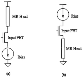
Several other design constraints are suggested by the literature. One such constraint is that when biasing the MR head, the head should be placed as close to ground as possible (Figure lb). This is done in order to avoid the buildup of a sizeable potential between the MR head and the hard disk surface, which could damage either the MR element or the
disk surface if discharged suddenly (Figure la) [6].
MR Head Ibias
Input FETInput
MR Head
(a) (b)
Figure 1: Options for placement of MR head
This means that current biasing sources should be placed between power and the read element, which in turn will connect to ground [1].
Finally, in actual practice, the preamplifier device will be amplifying signals read from a number of different drive heads. Multiple drive heads are often used, generally with one head dedicated for each of the platters in a hard drive. This implies that a multiplexer architecture must also be factored into the design. It is important to choose an architecture that degrades neither the noise performance nor the bandwidth of the original single head device [6].
3. Method
This section will describe the various methodologies used in the design and testing of the CMOS preamplifier.
3.1.
Design
The circuit design of the CMOS preamplifier was based closely on the existing Texas Instruments bipolar solution. For the new design, I started with the bipolar block diagram and then designed CMOS circuits to implement each of those blocks
The first stage of the bipolar preamplifier is the primary sensing unit, and is responsible for setting both the noise and bandwidth characteristics of the entire preamplifier. The main blocks within this stage are the transconductance (Gm) block, the Gm biasing block, and the input cascode tree (which included the MR head). The other crucial design block is the multiplexer circuitry, which allows the preamplifier to accept input from any one of eight separate MR heads.
The design is approached in a block-down style, which means that most of the circuit will be implemented with ideal components in SPICE until the circuit is made to function properly. Then, one by one, each of the idealized blocks will be replaced by an actual CMOS design that, when put in the circuit, produces the same result. For the first design pass consisted of the input cascode tree feeding into an ideal differential transconductance amplifier whose second input was an ideal voltage bias. Once this simple circuit had been perfected, the ideal transconductance amplifier was replaced with an actual CMOS circuit that mimicked the performance of the ideal one. Finally, the biasing was replaced with a bias current source that was mirrored to all the nodes requiring a bias current.
All circuit design was performed in Mentor using the Texas Instruments five volt 0.8gm BiCMOS process. Simulations were performed in TISPICE, a TI internal version of the SPICE simulation tool. TISPICE uses the BSIM3 algorithm to model transistor behavior.
3.2.
Optimization
Once the basic design was found to work, FET sizes and bias currents were systematically adjusted to procure the optimal speed and noise performance from the preamplifier. The optimization phase was done primarily to determine optimal sizing of M2 and R2 (Figure 11) with respect to gain, bandwidth, and noise. This was done by
holding all variables constant while varying one parameter (such as M2 width or length)
and running simulations that measured the gain, bandwidth, and noise. Once M2 was
optimized, the process was repeated to determine the ideal size for R2, and then to a lesser
extent, the ideal M, size and the ideal bias current level.
3.3.
Noise Measurement
The reduction of noise in the preamplifier circuit was of paramount importance, as excessive noise contamination inhibit the ability of the circuit to detect small input signals. In order to reduce circuit noise, a method first had to be devised to accurately quantify noise behavior by computer simulation. There were several possible options for accomplishing this goal. The accuracy of any such methods is ultimately dependent on the accuracy of the SPICE noise models for the process in question. This point introduces a degree of uncertainty into the picture that will be addressed later.
The criteria for a noise measurement method were straightforward. First, the method had to be quick and easy to perform, as dozens of noise measurements were often performed at a time. Secondly, the method had to be an accurate single number representation of the noise performance. It may seem overly simplistic to reduce a noise simulation taken over two or three orders of magnitude to a single number. However, in order to facilitate quick and objective comparisons between noise performances of different circuits, a single figure of merit was necessary.
SPICE offers two techniques of deriving noise performance information about a circuit. The first involves injecting non-deterministic noise at the input of each noise contributing
device and then summing the resultant noise at a specified node. This results in a time domain transient sweep. It was found that this sweep was slow to simulate and difficult to interpret due to the non-deterministic nature of the data. The second method SPICE has is to place an AC source equal to the equivalent input noise for each device at the input of that device. The user specifies both input and output nodes where the noise is to be summed. SPICE produces an AC analysis reflecting the summed input referred noise. Since this simulation is easy to set up, quick to execute, and produces useful data curves, it was selected. A typical input referred noise curve is shown below.
Input Referred Noise
-0.4. a: 0.2 0 1 106 108 frequency (Hz)
Figure 2: Typical input referred noise curve
The goal now is to reduce this curve to a single figure of merit that accurately quantifies its noise content. One approach is to pick a fixed frequency and read off the noise value at that point. This approach was ignored however because it varies too much from run to run. For example, changing a transistor size will affect the frequency response of the signal. Since input referred noise is divided back from the output by the frequency response, a change in frequency response alone at a specific frequency may be incorrectly interpreted as a change in noise performance at that frequency.
Another approach is to scan for the minimum noise measurement. This idea, while reasonable in theory, proved cumbersome to measure. Furthermore, it does not reflect the noise characteristics at all frequencies, but merely at one point.
A better idea was to calculate a simple arithmetic mean of the data. This idea failed for two reasons. Primarily, the signal plotting software SIMGRAPH does not automatically perform arithmetic means on signals. In order to compute the mean, each signal file must be manually edited, read into MATLAB and averaged there. This was unacceptably complicated. The second draw back of this method was that because the data is produced logarithmically, it becomes difficult to procure an accurte mean. An arithmetic mean taken on geometrically spaced points will be weighted disproportionaltely in favor of lower frequencies.
Finally, after consulting Jim Hellums, the noise analysis expert at Texas Instruments, an acceptable procedure was devised that works by feeding the SPICE analysis output file into a TI internal C program named INTNOISE, which integrates the noise relative to its logarihmic frequency axis. This procedure is quick, easy to execute, and uses every point in the noise analysis. Furthermore, the resulting figure of merit is acutally a quantification of the noise power over the bandwidth in question.
The only caveat about this method is that it is essential to determine the frequency band over which the input referred noise is to be integrated. Since the circuit will never be used outside the boundaries of its -3dB bandwidth, the noise must only be integrated within the -3dB points. However, since the -3dB points tend to shift from simulation to simulation with changes in the circuit, two arbitrary limits were set for the frequency: 1MHz < f < 100MHz. These were picked because they always contain most
of the valid frequency noise data. Thus, in order to procure the desired noise analysis, a typical SPICE stimulus file would contain the following lines to measure noise.
.noise v(out2,outl) vmr .ac dec 200 le6 100e6 .punch noise inoise
In order to determine a benchmark against which to compare noise performance, the originally stated benchmark of 0.5nv/--z must be integrated:
vi = 0.5nv/,H-z vi2 = 0.25 .10- 18 v2/Hz
JOOMMHz
0.25 10-18 v2/Hz df = (0.25. 10 -18). (99. 106 2 = 0.2475. 10-10 v2 = 4.98vTherefore, 4.98gv is a valid equivalent benchmark against which to judge circuit noise performance when measured using the INTNOISE function. To check the calibration of the INTNOISE function, a constant of 0.5nV was integrated over 1MHz-100MHz using INTNOISE. This produced a result of precisely 4.98gv. The result is consistant with the prediction, and so INTNOISE is assumed to be accurate. A more interesting benchmark is achieved by measuring the integrated noise in the Bipolar design. This is a more consistent estimator. The integrated simulated noise in the existing bipolar first stage unit is actually 12.9gv, or roughly 1.3nv/VHz. Therefore, a sufficiently quiet CMOS first stage will have the same noise performance.
4. Noise Models
A substantial part of the research in this study involved the quantification and measurement of circuit noise. Therefore, it was necessary to understand the basic noise models upon which SPICE circuit simulations are based. These will be explained here.
The noise models used in the hand calculations of this study include only thermal and flicker noise. Other noise sources are ignored as their contribution to the overall noise performance is minimal and their elimination from the noise equations greatly simplifies the math. Thermal noise is associated with resistive components and is modeled as a voltage source of value
2
Equation 1 -= 4kTR
AI
in series with an ideal resistor, where k is Boltzman's Constant, T is temperature, and R is the device resistance. The noise is expressed as a square because it represents the noise power. The literature suggests that flicker noise is generated by random carrier trapping that takes place at the Si/SiO2 interface [7]. Flicker noise is defined as a current source of
value
i2 a
Equation 2 KI b
Af fb
in parallel with the element in question, where K is a device constant, I is the direct current,f is the frequency, and a and b are constants.
These noise models are added to standard AC small signal models for bipolar and FET devices to produce device noise models. To simplify circuit analysis in subsequent chapters, all noise sources in a given transistor are referred back to the gate or base (the transistor input) and consolidated. The following figures show the resulting AC noise models for both FET and bipolar devices that will be used for noise analysis later on.
SI I I I
Figure 3: Bipolar small signal noise model
Figure 3 shows the bipolar small signal noise model. For a bipolar device,
v2 = 4kT r+ . Figure 4 below shows the FET small signal noise model.
2gm
i2
.gm*vg
+C vis vg rds
p p
Figure 4: FET small signal noise model
In the case of the FET noise model, the input referred voltage noise can be broken down into the sum of thermal noise and flicker noise. The most accurate expression for thermal
2 8 kTAf, has been found to be
noise is disputed. The most popular expression, Vn,themal 3 gm
inaccurate, especially in the triode region and when Vds =0. A more accurate thermal
2 y4kTgdoAf 1- +P 2 VIn
noise model is nhel 2 where y = and [7]. g do
gm 1- l
Vgs -V,
is the expression for channel conductance at zero drain to source voltage. As the transistor approaches saturation, y -4 -, and thus the thermal noise expression reduces to
8 kTgdof
2 8 kTgdof . This equation is valid as long as short channel effects do not affect
n'theml 3 T- gm 2
2 KfAf
the FET. FET flicker noise is given by v ,icker - 2f respectively.
5.
Existing Bipolar Design
This section will explore the architecture of the existing Texas Instruments bipolar preamplifier. The preamplifier is a three stage structure, and only the first stage will be analyzed here. Multiplexing circuitry is also ignored here. The idea is to provide an analysis of the single head first stage bipolar circuitry so that it can be compared with the design of the single head first stage CMOS design. The analysis results of this first stage determine the design parameter goals for the CMOS design.
5.1.
Schematic
Functionally, the bipolar first stage produces a differential output voltage that is
AJRm
proportional to mr , where ARmr is the incremental change in MR impedance, and Rm Rmr
is the nominal DC MR impedance value. A circuit topology producing such a dependence protects the circuit output from drifting if the nominal head impedance should change over time with temperature or head wear. A simplified schematic of the existing stage one circuitry appears below in Figure 5:
Vee k Rload --0 + Q2 -Vat Q3 D Vbias Q A B Q4 ias Gm C QS Ibias Cs V Idac
ih
Ci
/
.
IV
5.2.
Functionality of Schematic
5.2.1. DC Bias Points
As shown in Figure 5, the primary circuit structure of the existing Stage One preamplifier is a feedback loop that is used to bias transistor Q5 such that the DC differential output voltage is zero volts. The feedback loop compares Va to Vb. If they are not equal (ie
Vout 0), the transconductor Gm generates a current proportional to Vb -V, that either
charges or discharges the capacitor C1 (depending on whether or not Vb > Va ). As the
voltage across C1 changes, the voltage bias on Rn changes accordingly (because Qs is an
emitter follower) thus forcing Vb to change as well. This process continues until Vb = Va,
at which point Gm stops producing current, and the cycle is broken.
Once the DC bias points have been established, the circuit detects and amplifies small changes in the impedance of the MR head. Instead of discussing the circuit response to small changes in Rmr, it is more intuitive (and computationally simpler) to consider the equivalent stimulus of AVmr, namely small deviations in the voltage across Rmr. This AVmr signal is amplified by the resistor tree by a gain of -150/Rmr, to produce the signal Vb at node B. Since the output signal is Vb -Va, the Stage One output is simply the differential signal V,,U = (150/Rm,) AVm, .
It is important to note that since AVrn is an AC signal, the AC current it will force the Gm stage to produce will short circuit through C1 to ground, hence not disturbing the DC bias
point on the base of transistor Q5.
This circuit topology has several key strengths that make it suitable for its application as a preamplifier. One such strength is the ability of the feedback loop to compensate for drift in the nominal DC Rm, impedance of the MR head. Should Rmr drift over time with either temperature or head wear, the feedback loop automatically adjusts the bias points so that the DC differential output voltage returns to zero. Furthermore, since the output
voltage is proportional to ARmr and inversely proportional to Rn, the circuit output tends to reject Rmr drift. This is possible because when Rn drifts, ARmr will tend to drift as well, and so the ratio of AR., IRm, will remain close to constant.
5.3.
Bandwidth
The existing Stage One preamplifier has a bandpass frequency characteristic. The low frequency pole is produced primarily by the transconductor Gm and the capacitor C1. Consider the following simplified block diagram of the feedback loop shown below in Figure 6: + Vb deltaVnr Vmr -150 R1 r + Vcl
Figure 6: Feedback loop block diagram
From Figure 6, it is evident that:
Vb - 150/Rm, (s) AVmr 1+ 150gm sRmr Cext 150s/Rmr + 150gm RmrCext
The equation dictates a system zero at s = 0 and a left half plane (BIBO stable) pole at S-1 50g . To verify this prediction, a SPICE model simulation of the preamplifier
was executed, varying the parameter C1. Comparisons of the predicted pole locations versus the actual locations are shown below in Table 1 based on the parameters
Rmr = 30L and Gm = 5.6x10⁻³ 2- :
C1 f3db(predicted) f3dB(simulated) Error
5nF 807 kHz 792 kHz 1.9% 10nF 404 kHz 390 kHz 3.5% 20nF 202 kHz 197 kHz 2.4% 50nF 80.7 kHz 78.0 kHz 3.5% 100nF 40.4 kHz 39.4 kHz 2.4% Table 1
The calculated breakpoints take into account the emitter resistance of Q5 in series with Rmr. This parasitic resistance is calculated as:
1
Re,Qa
where
g 5Im,Q
Vth
refers to the tranconductance of transistor Qs. The error between the actual breakpoints (from the simulation) and the predicted breakpoints (from the hand calculations) is most likely due to transistor parasitics not taken into account in the hand calculations.
The location of the high frequency pole is due primarily to an impedance divider at node D between the 150Q resistor Rload and the collector to substrate capacitance of Q4, shown below in Figure 7:
Vcc
Scs Q4
Q3
Q4 Vbias
Figure 7: Source of high frequency node
The capacitor shown in Figure 7 is actually a sum of two parallel capacitances:
cs,Q4 cs,intrinsic cs,sim
Cos,intrinsic refers to the intrinsic collector to substrate capacitance of transistor Q4, while Ccs,sim is a dummy capacitor added to the computer model solely for the purpose of being able to vary Cos in order to verify pole location predictions.
In order to determine the high frequency pole location, Figure 7 is redrawn for an AC analysis. Because all DC sources are AC grounds, Vcc goes to ground, and Figure 7 reduces to:
Figure 8 : AC model of the high frequency node
Vd = I(s) (150K II 1/sCc )
= 1s+lCcs -I(s)
The current source, I(s), is generated by the AC input voltage, AVmr, divided by the resistance of the MR head, Rmr:
I(s)
-Rmr
Substituting for I(s), it is evident that the predicted pole location is at
-1
0 = . This prediction was verified with SPICE simulations that
(R2 = 1500) -Ccs,Q4
varied Ccs,sim. The first simulation was performed with Ccs,sim = 0 in order to empirically determine the Cc,intinsic value of Q4. The remaining simulations verify the high frequency pole locations. Table 2 summarizes the results of this simulation:
Ccs,sim f3dB (predicted) f3dB (simulated) Error
OpF 1/(27. 150-Ccs,intrinsic) 2.11 GHz lpF 707 MHz 790 MHz -10.5% 5pF 193 MHz 201 MHz -4.0% 10pF 101 MHz 105 MHz -3.8% 20pF 51.8 MHz 53 MHz -2.3% 50pF 21.0 MHz 21.5 MHz -2.3% Table 2
Ccs,intrinsic is therefore estimated to be 0.5pF.
Figure 9 shows the overall transfer characteristic of the circuit. It is worth noting that at low frequencies, the frequency response increases at +20 dB/decade, verifying the claim of a zero at o = 0 and a low frequency pole at
f3dB =
(R2= 150) (gm = 5.6.10-3 -180Hz. 27r -(Rmr = 30 ) -(C = 22nF)
The high frequency rolloff is slightly steeper, which indicates the presence of some other high frequency pole, most likely due to parasitic capacitances within either
Q4
or Q5.111111 II 1111111 I 1111 II1111 111111 I I 111 I111111 S I I I IIO I I I )I I I I I I III I I I I II I I1 1 I I I I I Iii a a saI I I I I III a ii 11111i I I fl . . . ... ~: . . . .iJ.. : .I ~ . . I: . .M.. . . . .. .
I I I1 11 1 1 1111 i I Ii1 i I I 11111 i I 1 111111 111111 i1I i I IIIIi 1 1
I 111111 1 11111 1 I Il I l I 1111 I I 11111 a 1 1 11I I 11111I
i I 1 111 1 1 1111 11i1111 11111 11111111 1 11111 i I 1 11115 1I 11 il
l i i Ill i 1111111 1 I1I1 1 I I i I 1 11111 I SIII I I I II I I I I I 11111 I I i I a Il a aI II II II I II II III
I I I " M I I fi I I IIII I I I 1 I I I f I Iiii I I I I II
I I I Iif I 111111 1111111 111111 I 1 II I I itII I I III I 111 I I I I 1111 I 1111 1 I 1 aa 111111 3 111 5 11111 I 111111 I I III1 I l Il l I II II I I ll a I Il
. ... , . 111111 . ... .. 1111 1 111. .. 1 I . .1.1111 .I 111111 .. 3 i1 l I 1111111 I 1 11111~ I 1 1111(11 I 111)111 I 111111 a I 111111 I 1 1111 1 11111 I rIt i a , a aiia1 111111 II / a a aaaaaa1 a hau a a ilI iilill I a aia 11(111 11111111 1 1 1111j 1 1111111 1111111 It I 1 1111n1 Il~t 111(11 I ara I11111 I 111111 II) I 11111 I 1 11 I 1 1119 I 1 111111 I 111111 I 11111( I 111111 I 1 111111~ Itl 11111111111 1 (ll I 11111 1 111 1111 I I 11111 1 I II) I 1 111111 1 111111~ 1 111111 I 11111 I 111111 Ltl
I I 11111I I I I I I I111 I 1111 111111 II I II I 1 11 I 1111111 I I 111111 I 111111 I 111111 I 11111 11 I 1111
I 1 1 l l I I I I II1 I I II I I III 1 I I~1( III I I111 I 1 III 11 I I 1 I1 I III I I I I I I I IIII I I I I1111111 I I I I I 1111 I l ll 1 11 1
I 11 1 II I I 111 1 I I 111111 I I III I I s III a 1 I11111 I 1 1111 I I I I IIII I 111111 I I 111 1 1 1 I I111111 I I 111111I
I I iIIII I I. I I IIIII 1111111 I I II j jlllll .J .J l Ill
111111 1111 1 III( 1 f11111 1 I lty 111111 (I)~t 1 (( t11111 S1111 I I II I II I 11111 I II IIIII1 I 1 I 11111 I 11111 I I 11111 I I 111111 I Ill I r I I 1 11111 I I I I 111 I IIII I I I I 1111111 1 1111 I I I 111 i|I 1 1 111111 a Ill a)11 sai II a I a111 1 111111 I 1 111111 1 11111 I 111111 1 1111111 1 111111 5 11111 I 5 111111 1 )1 I 111111111111
1 iiii i I i11 i i i i i1111 1 1 1 11111iiI 1111 i 1 11111 1 11111
I I I i i11111 I I i i 1iii I 1 1 1 11i 111111
1111 II 1111 111(111111111,1 a imlll lallas 5 )1111 1 111111
I I i i 11111 i i i i111111 i i i1 i i i 1111i1 i 11111i 111111 I I i11 ii i I iii 11 1111 I 11111 1 IIIll 1 111111
1 ~1( 111111 111111 1 1 111111 1 111111 I 11111 I 111 I 111111 I I I I I 11111 i i i I 1111 I 1111111 I 111111 I aai i aa i 11111 i 1111 I i iiii I i IllII 1 111111 I1 II Ii I I II 1 1Ii I II 1 I 111111 I I i ii I I iiiii I i i iii i I I iiii 1 i 111111 i a alaII I
; t ; II iI I iiiii1 I i I1 i ii rrm 1 1 ~rm-rrm I I iII I Ill ~ l I I IIII11 ~nm-~rn I I I II II I II IIII rrimI I I I I
I iiiii1i1 I ii i I i1 1: 1 11I i I I II I I II I I al 1 l aii a aI la 51 11IIit i I i i i i i ii i i i 1: i i i 11 i i i ii i 1 l l i I i i l i 1 i i i
ii~ ~ ... .... ~ ~ ~ ... ~ ~ ~1U .... . '... . .. ..
100 1K 10K 100K 1M
HERTZ
Figure 9: Bandpass characteristic of the bipolar preamplifier circuit
1 11111(11I I IIII11 I I IIII11 SI I II II Vout Vmt 0 -7 -14 -21 -28 -35 -42 -49 ... 1 i i I III I i I iii i i i i ii 1UUM IG I 1UM
6. CMOS Design
This section will describe the block by block design of the CMOS MR preamplifier that was the goal of this research. As described in the Methods section, this task is most conveniently broken down in design of stage one, design of stages two and three, and design of the multiplexer architecture. The multiplexer architecture will be explained after the first stage predicted behavior has been derived. This is done to reflect the fact that the multiplexer architecture will debilitate performance regardless of the quality of the stage one design.
6.1.
Stage One Design
The first stage of the bipolar TI design is responsible for biasing the MR head and detecting small variations in the resistivity of the head. These variations are converted into a voltage signal and then amplified by a small factor. Two different approaches were considered for solving this problem in CMOS. The first was a design based on an article by Klein and Robinson (K&R) that used a current mode solution. The second approach was to use the TI architecture by replacing the bipolar components with FETs. The K&R approach, while offering the promise of superior bandwidth was ultimately rejected, as it was too complex relative to the TI approach and much too slow. A brief review of the K&R design considered as a solution will be presented in the Appendix.
A block diagram for stage one is shown below in Figure 10. This design is based mostly on the TI bipolar circuit:
Vdd R2 Voltage bias Gm M2 input FET Cl MR element
Figure 10: Stage one block diagram
Ideally, the voltage bias feeding into the left input of the transconductance (Gm) block will cause the feedback loop to keep increasing the drain current in M2 until the voltage
vout- equals vout +. At that point, the Gm block stops producing current, and so the
M2 gate stops increasing in voltage.
A simplified version of the stage one schematic is shown below in Figure 11. It is simplified in that the multiplexer circuitry is not included. A schematic symbol is used for Gm, and is expanded completely in Figure 12.
Vdd
out
-
M5M6
o
M7 M8
Figure 12: Voltage controlled current source transconductance amplifier
In Figure 11, the circuitry to the left of the Gm block, consisting of the DAC current, R1,
C2, rbias, and M3, are used to set the bias current of the main input cascoded tree on the
right. The biasing circuitry produces a bias drain current in M2 of Idac, -L . Furthermore,
the DC bias of vout+ and vout - is Vdd - IdacR. The user is typically allowed to adjust
this bias current by means of adjusting the Idac current via several control bits. This mechanism was beyond the scope of this design. Thus, Ra has been biased. As Rn varies in time, the biasing current running through it remains constant, and so the voltage at N1 changes accordingly in time. This AC AV signal is amplified by a ratio of R2 to node vout -. Taking the output as the differential signal (vout +) - (vout -)
R +'
Rmr
gn2
subtracts out the DC bias level, Vdd - IdacRl. The capacitor C1 sets up a GmC filter that shorts all high frequency signals to ground, allowing only low frequency components to set the bias by altering Vgate,,,,M2 C2 is used to remove all the high frequency noise
generated by M3 and R1. Without it, the biasing branch becomes a significant noise
contributor. Since the bias signal is not changing in time, a large C2 Will not affect the
system gain or speed. The resistors rbiasl and rbias2 are resistors that serve to set the gate
spike. In that event, each of those resistors in series with its associated FET capacitance will form an RC filter to low pass filter the power spike and protect the device. Finally, the cascode FET M1 is included to increase the impedance of M2, effectively helping
reduce the short channel effect in M2.
The voltage controlled current source Gm block is a standard differential input transconductor that works by mirroring current around from each of the inputs to the output node. The transconductance is set by the bias current and by the ratio M1 : M2.
6.2.
Stage One Predicted Behavior
-
Transfer Characteristic
Equations can now be derived to predict the band pass behavior of the circuit. This is accomplished by separately analyzing the midband gain, the low frequency pole, and the high frequency pole.
6.2.1. Midband Gain
The midband AC gain is set by the ratio R2 . This can easily be seen through two
Rmr g+ simple equations: VNl Equation 3 1drain,M2,AC Rmr + R + 1 vout -Equation 4 Idrain,M2,AC R R2 Combining Equation 3 and Equation 4, it is found that
VN, vout
-R mr + gm2 I R2
vout - R2
Equation 5 .
There is no DC gain, as the output, taken differentially, uses the bias circuit on the left of Figure 11 to subtract off the DC component. The M2 FET degenerates the gain by adding
a parasitic resistance in series with the MR head resistance.
6.2.2. Low Frequency Pole
The Gm stage and the capacitor C1 define the low frequency pole, both of which are found in the feedback loop. The cascode branch, as well as the feedback loop can be modeled as a block diagram shown below in Figure 13.
V + -R2 Vout N1 Vm ir + 1 S Rnir + g i g 2 + Gm sC1
Figure 13: Low frequency pole block diragram The transfer function is now easily calculated:
VN1 VN1 Gm - R 2 V S sC 1 Rm + o 1 mr gin2 N1 Rm + sC9Rm2r R2 s(R + 1 Equation 6 - = VN1 s + GmR2 GmR2
This predicts a zero at s = 0 and a pole at s =- (R 1
Incidentally, at high frequencies, once the pole has sufficiently cancelled out the zero, the flatband gain is +2 I), which is precisely the midband gain predicted in the
previous section.
6.2.3. High Frequency Pole
The derivation of the high frequency pole is slightly more involved than that of the low frequency pole. It requires several simplifications and assumptions to make the math more tractable. The high frequency pole is defined primarily by the parasitic capacitances from M1 and M2. Consider the input cascode tree and its parasitic
capacitances: R2 _ R2 Mi _ M M2 M2 Rmr Rmr
0.
Figure 14 : Parasitic capacitances defining the high frequency pole
The system input can be modeled as an AC source feeding into a stationary Rn (instead of a resistor Rr varying in time) without loss of generality. This is reflected above in Figure 14.
An AC model based on the half circuit above is shown below in Figure 15. All of the parasitic capacitances are lumped into one of these capacitors. This is possible because both the gates and bulks of both the M1and M2FETs are at AC ground:
Cpl
-v gml1 il ni1<AV
Cp2 _ ci2 nrs2<v2
Cp3 Rmr O vinFigure 15: AC model for high frequency pole
where
Cpl = Cdgl + Cdbl
Cp 2 = Csgi + Gsb1 + Cdg2 + Cdb2
Cp3 = Csg2 + Csb2
The high frequency pole location is found quite easily by solving the following system of equations: - V0
- V,
= -vo gm •(v - v ds -v 0 - VO o= svICp2 v2gm + (v1 - v2)g - V0 R -c SV1C,2 = SV2C, + (v2 - in)To simplify the solution, it is assumed that gm, >> gds and gm2 >> gd2. Solving, it is found that:
gm, gm2 RmrCpCp 2 Cp3 Equation 7 A, = + S+ C+gm2 Cp2 p3Rmr Cp3 RC2 p1
The predicted pole locations are therefore
-gm, -1 1 -1
Equation 8 - C ,P2 R + 2 P3 =
This equation makes sense intuitively. Primarily the parallel RC combination of R2 and C,p sets the -3dB point. Cp2 and Cp3 also contribute to the bandwidth, although to a
lesser extent. SPICE simulations revealed that increasing R2 linearly decreases the
bandwidth linearly. Increasing the width of M2 linearly produces a decrease in the
bandwidth that is roughly cubic. Increasing W2 from 1000Lpm to 5000gm produces a
reduction in bandwidth of 70%.
Finally, note that from Equation 7, if s is small (i.e. well below the -3dB frequency), then gm gm2 RmrCp lCp 2 p3 av= gmi 1 + gm2 Cp 2 nCp 3Rmr Cp3 2Cp R2 R mr +'gm2
Thus, the predicted midband gain is the same as that predicted in the two previous sections. This is a good sanity check.
6.3.
Stage One Predicted Behavior
-
Noise Performance
Simulated circuit noise can be predicted accurately using standard CMOS noise generator equations. In this chapter, the CMOS noise models in Section 4 will be used to derive expressions for noise that will be verified with SPICE simulations. Only thermal and
flicker noise sources will be considered, as they are the primary noise sources in FET devices.
6.3.1. Primary Noise Contributors
Most of the input referred noise in the circuit is produced within the component tree consisting of the gain resistor (R2) the cascode FET, Ml, the input FET (M2), and the MR
head (R,): R2 M1 [Vb v2 vi [IM2 il Rmr
Figure 16: CMOS reader half-circuit
The noise produced by the MR head is independent of the quality of the circuit and will always be present. Hence, it is omitted in all subsequent calculations.
vO -v2gmC rd 1 v2 -i22gm2 1 rds2 i2 Rmr vi
Figure 17: AC equivalent of reader half-circuit
The total noise current can be expressed as the sum of the noise currents in the resistor and each of the two FETs:
.2 .2 .2 .2 Ion, = I +'M2 + lr2
And since .2 = gm 2v
.2 2 2 2 2 .2
Equation 9 Ion = gmleff Vn + gm2eff Vn2 + 'r2
In order to evaluate this equation, expressions will be needed for gmleff and gm2eff.
6.3.2. gm2eff
i
vi
-i <R
Figure 18 : AC Equivalent Circuit for Solving gm2_eff Equating currents from Figure 18, it is quite easily seen that
i = -iRgs + gm(vi - iR)
Equation 10 i[1 + Rgds + gmR]= gm -vi
Since gm >> gds, Equation 10 reduces to
Equation 11
gm
gm2eff v
i 1+ gmR
This is the phenomenon known as source/emitter degeneration.
6.3.3. gmleff
vi MI v2 Vb M2 i R gml(v1-v2) -iRgm2 rds 1 1d52
Figure 19: AC Equivalent Model for Computation of gml_eff
In order to solve for gmleff , two equations for v2 will be equated. The first is
i = -v 2gsl + gm, (vi -- 2) Solving for v2 and assuming that gm, >> gds1, it is found that
Equation 12 V gmlv. -i
2 =i gm
Using M2 for the second v2 equation produces:
i = (v2 - iR)gds2 - iRgm2
Using the same assumption as before about g ds2 results in
Equation 13 v
2 =irds2 (1+ Rgm2)
Equating Equation 12 and Equation 13, and solving for gmeff produces:
Equation 14 gm 1 +
+
Rgv1 l+gmrds2(l+Rgm 2)
This result makes sense intuitively, as it represents a recursive application of the source/emitter degeneration demonstrated in Equation 11.
6.3.4. Thermal Noise
It is now possible to write equations predicting the majority of the thermal noise present in the circuit. The reason that only a majority of the noise is accounted for and not all of the noise in its entirety is that several noise contributing components in the feedback path have been completely ignored in the noise analysis. This is done because their noise contribution referred to the input, relative to the other noise contributors, is minimal. Furthermore, their omission greatly simplifies the noise equations.
Combining Equation 9, Equation 11, and Equation 14, as well as the fact that the input
2 8.kTgdo
referred voltage thermal noise for a FET is ,therma (Section 4) it is shown
that
2 = f 2 2 2 *2 ion = gmi vn, + gm2eff V,2 R+ R
gmi 8 kTgdo,1 g 2 8 kTgdo, 2 4kT 1+ gmirds2 ( g 2 rmr) 3 gmI2 Af rmr M2 gm2 r g4k2 9do,l 2 gdo,2 1 34 [1+ gm rds2 (1+ rmr g 2 )]2 3 [1+ rgm2 r2 2 .2
and finally, since Af = rmr AIon
Equation 15 2 [2 rdo,l
2 do,2
vn = 4kTr2r g ,1 1 ]2
Af 3 [1+ gm1 rds2 ( + rmr 9M2 )]2 3 [1 + rmr gm2 2
6.3.5. Flicker Noise
Input referred flicker noise is calculated in much the same way as thermal noise. The input referred flicker noise for a given FET is
v2 K
Equation 16 f
Af WLCoxf Note that there is no flicker noise present in resistors.
Equation 17
f
M1r(+gm 2r Af 1+ gm r,, (1+ gm2rmr ) KFN gm 2S2COxWLf
+ r,,+rgm 2SW
21d ACo -, Equation 17 becomes L .2 KFN Id A f L(1+
gml rd2 (1+ gm2 r ))2 2 .2 and since = r2r on Af If "o KFNrIfl d ( 1 Equation 18 - g ( m ))2 Af f +, 9?I r2 (1 + 9M 2 r l d j(l+ rgm2 4 (1+ r-gm2)2Equation 18 is used to calculate a flicker noise curve for a (-) FET (to predict flicker noise from the M2 FET), as shown below:
xlOl 7
5
3 \ 1 10i 10 10' Fmqency(F4 10 10'Figure 20: Predicted Input Referred Noise Curve
6.4.
Verification of Noise Calculations
As will be shown in Section 7, the primary noise contributor to the circuit will be flicker noise from element M2. In this section, it will be shown that the hand calculations for M2
flicker noise agree with the TI SPICE models.
The term for M2flicker noise is derived from Section 6.3.3:
Since gm =
KF, 2CoW2L2 f
2 K 1
2,M 2flicker Kf 1
Equation 19M 2flc
Af WLCx f L2(1+ ,mrgm2)2
Equation 19 shows that, to a first order approximation, M2 flicker noise decreases as the inverse square of gm2. By formula, gm2 can be expressed as
Equation 20 gm2 = 2 1
d Cox 2,
L2
Equation 19 and Equation 20 together show that (to a first order approximation) M2
flicker noise is inversely proportional to Id 2 . Thus, it is expected that if W2 is
L2
increased by a factor of four, then gm2 will be doubled. Furthermore, if gm2 is doubled 2
when L2 =1 pm and rmr = 30U, then vM2flicker is reduced by a factor of
4f
L
(1
+ rmrgm2ol 2 = 0.47 at every frequency, where rmr = 30 , gm2old = 28.3mS (for
L2 (1+ rmr gm2new )2
M 2 1000 ), and gm2new = 2gm2old . To incorporate this finding into integrated noise
2
savings (integrated noise being the noise standard used in this thesis), the following integration is performed: 100MHz noiseold =
f
C df = 2C 1MHz f 100 MHz noisew = f 0.47C f df = 2C(0.47) 1MHzf
where C is a lumped constant of all the other coefficients in Equation 19. Therefore, the reduction in integrated noise is a factor of
noisen 2C 0.047
noiseold 2C
Thus, if W2 is quadrupled, the hand calculations predict that the total integrated noise will
be reduced by a factor of 0.47. To verify against the SPICE models, we will compare this prediction with the total integrated noise from Table 7 for W2 = 1000pm and