Advances in the CVD growth of Graphene
for electronics applications
by
Mario Hofmann
Dipl. Ing. Technische Physik, Technische Universitat Ilmenau (2006) Submitted to the Department of Electrical Engineering and Computer Science
in partial fulfillment of the requirements for the degree of Doctor of Philosophy
at the Massachusetts Institute of Technology February 2012
0 2012 Massachusetts Institute of Technology. All rights reserved
MASSACHUSETTS INSTITUTE OF TECHNOLOGY
MAR
2
0 2012
LIBRA RIES
ARCHIVES
A u th o r... . ... ...Department of Electrical Engineering and Computer Science, October 23, 2011
Certified by... ...
Jing Kong Professor of Electrical Engineering and Computer Science Thesis Supervisor
C ertified by ...
Mildred S. Dresselhaus Institute Professor of Electrical Engineering and Physics Thesis Supervisor
C ertified by ...
Michael S. Strano Professor of Chemical Engineering Thesis Supervisor Accepted by...4eslie S) 4lodziejski
Advances in the CVD growth of Graphene
for electronics applications
by
Mario Hofmann
Submitted to the Department of Electrical Engineering and Computer Science in partial fulfillment of the requirements for the degree of
Doctor of Philosophy
ABSTRACT
Graphene, a monoatomic sheet of graphite, has recently received significant attention because of its potential impact in a wide variety of research areas.
This thesis presents progress on improving the quality of graphene for electronics applications. An analysis tool was developed that provides a fast and scalable way to reveal the defectiveness of CVD grown graphene. This approach relies on a graphene passivated etching process that was found to be sensitive to structural defects in the graphene film. A strong correlation between the density of structural defects and the
electron mobility emphasizes their importance for high quality graphene devices. The dimensions of graphene defects were found to be nanometer-sized and it was
demonstrated that the defects exhibit novel fluid dynamical properties.
The graphene synthesis process was investigated using the described analysis tool and the kinetics of graphene formation was revealed. The influence of promoters on the growth process was described and analyzed.
The new insight into the growth process was applied to a novel approach to directly synthesize graphene patterns by catalyst passivation. Several advantages of this method over existing fabrication schemes were described and a number of applications based on these improvements were shown.
Acknowledgements
I want to thank my advisors, Professor Mildred S. Dresselhaus and Professor Jing Kong,
for offering me the opportunity to do research in their groups, for their support and for being role models in many more fields than science.
I am very grateful for the chance to interact with many amazing people during my stay in
MIT and Boston:
e Lab mates, who taught me not only skills but excitement for research.
* Friends, who made Boston less gray and Wednesdays more exciting. * Collaborators, whose effort improved my work and understanding.
* Supporters, who helped navigate the challenges of student life. * Visitors, who shared their culture and broadened my view
* Students, who taught me while I trained them.
0 Hosts, who opened new worlds to me.
Meiner Familie sei gedankt fUr ihre Unterstfitzung. Finally, I want to thank you for your interest in this work.
Table of Contents
1. In tro d u ctio n ... 1
1.1 History and future of graphene... 1
1.2 O utlin e ... . . . 7
1.3 F undam entals ... . 8
2. A facile tool for the characterization of CVD grown graphene... 23
2.1 Necessity for a new analysis tool... 23
2.2 Concept of graphene passivated etching ... 24
2.3 Experimental results ... 25
2.4 Quantification of graphene defectiveness ... 27
2.5 Information about the substrate... 29
2.6 Comparison to Raman spectroscopy ... 31
2.7 Effect of defects on electrical transport... 34
2.8 Challenges of the analysis technique ... 36
2.9 Sum m ary ... . 37
3. Study of structural defects in CVD grown graphene... 39
3.1 Observation of graphene defects ... 39
3.2 Measurement of graphene defect size ... 40
3.3 Generation of lattice defects... 42
3.4 Fluid dynamic behavior of structural defects... 43
3.5 O rigin of defects... 5 1 3.6 Minimization of graphene defectiveness... 55
4. The effect of promoters on the growth kinetics of CVD graphene... 57
4.1 Application of graphene passivated etching to growth studies... 57
4.2 Catalyst poisoning during graphene growth... 59
4.3 Graphene growth kinetics... ... ... 61
4.5 Experim ental confirm ation of m odel ... 64
4.6 Com parison of prom oters... 71
5. Direct CVD synthesis of patterned graphene via catalyst passivation ... 76
5.1 Prior art... 76
5.2 Experim ental results... 78
5.3 Applications in functional devices ... 81
5.4 Analysis of graphene patterns ... 83
5.5 Deposition m ethods... 85
5.6 Graphene based devices on com plex surfaces ... 88
6. Conclusions... 92
6.1 Future work... 93
6.2 Outlook... 95
List of Figures
Figure 1 Depiction of graphene ... ... ... ... ... 1
Figure 2 Timeline of discoveries made in relation to graphene -9 ... 3
Figure 3 NSF funding for carbon materials vs. time ... ... ... 5
Figure 4 Required m aterial to produce graphene... 10
Figure 5 Schematic of the CVD setup used for graphene growth ... 12
Figure 6 Schematic of homebuilt ALD system in the nmelab... 15
Figure 7 Optical micrograph of graphene and various thickness multilayer graphene... 17
Figure 8 AFM images of graphene (a) false color representation with estimate of number of layers (b) 3D representation of sam e im age ... 18
Figure 9 Publications for carbon related Raman spectroscopy normalized by total number of all Raman related publications... . ... ... 19
Figure 10 Representative Raman spectrum of Graphene and indication of common features ... 20
Figure 11 Raman map of the G'-band FWHM of a graphene flake, (inset) optical image of the same flake 21 Figure 12 Schematic of the graphene passivated etching process: In the case of complete graphene coverage (upper panel) no etching occurs but openings in the graphene film result in etch pits in the copper substrate (lower panel). (b) Optical micrograph of copper surface after 10s etching with complete (top) and partial (bottom ) graphene passivation layer... 26
Figure 13 Morphology after 10s etching for 3 different growth conditions by optical microscope (a-c) and AFM(d-f) images: (a,d) no graphene growth (0=1%) (b,e) incomplete graphene film (0=30%), (c,f) complete graphene film with a low density of openings (0=95%)... 29
Figure 14 (a) AFM image of aligned etch pits, (b) orientation of crystallographic planes (c) 3D representation of AFM close-up of one etch pit, (d) 2D Fourier transform of (a), (e) SEM image of two areas w ith different shaped etch pits... ... ... ... ... 31
Figure 15 (a) Unetched area 0 as a function of UV-ozone exposure, (b) comparison of Raman ID/Ic ratio and 0, (inset) representative Raman spectra at various exposures... ... ... 32
Figure 16 (a) Maximum mobility and corresponding sheet resistance for devices within an interval of graphene coverage. The insets show representative AFM images after 5s etch of graphene devices corresponding to the low and high mobility cases (scale 20x2O m2)... 35
Figure 17 (a) Optical micrograph of graphene transferred from the etched and unetched parts of a copper substrate, (b) Raman spectra of etched and unetched graphene areas showing identical results... 37
Figure 18 (a,b) Schematic of the analysis technique: (a) copper etchant is applied to a graphene sheet (b) holes in the graphene are permeated by copper etchant and generate etch pits in the Cu substrate, (c) AFM height image of graphene passivated Cu after a 10s etch ... ... 39
Figure 19 (a-c) Representative AFM height image of etched graphene (a) without, (b) with a 5nm ALD film, and (c) with a 16nm ALD film, (d)Relative copper hole area vs. deposited ALD film thickness for pristine and U V -ozone treated graphene film s ... 41
Figure 20 AFM images after 45s exposure to UV ozone before (a) and after (b) 10s etching. Squares indicate holes correlated with the position of a particle, circles are holes without a discernible particle... 43
Figure 21 Dimensions (depth and diameter) of one etch pit vs. etching time with linear fitting. (Insets) Morphology of the same graphene sample after 5s (top left) and 35s (bottom left) of etching with indication of the m easured etch pit (arrow )... 44
Figure 22 (a) AFM height image of graphene passivated SiO2 after 30s buffered oxide etchant, (b) Spatial Raman map of the G-band intensity, indicating the presence of graphene throughout the sample, (c) overlay of etch pit boundaries obtained by AFM (bright lines) and Raman D-band map (colored areas)... 46
Figure 23 Comparison of etch rates of bare copper substrate and etch pit depth of graphene passivated co p p er su b strate ...- ...----..- . 4 7 Figure 24 AFM image of region before (a) and after lOs etching(b), lines indicate location of wrinkles b efo re etch in g ... . . ----... 4 8 Figure 25 (a) Evolution of the area of one etch pit and fit, (b,c) two representative pictures and an indication of the tim e each im age w as acquired. ... 50 Figure 26 AFM height images of the same location on a graphene passivated copper sample (a) before etching, (b) after 10s etching, (c) overlay of both images with an indication of proposed type of defect, (inset) types of defects resulting in etch pits: (1) nucleation region and (2) surface imperfection, (d) AFM
amplitude image of the same area as (a-c) before etching, (e) depiction of different textured regions in (d) w ith indication of the presence of bilayer regions... 52
Figure 27 (a) Optical microscope image of a graphene sample identical to the one in Figure 26 after transfer to Si/SiO2. Bi-layer graphene occurs as darker islands on the continuous graphene sheet. (AFM scan size of Figure 26 is indicated as rectangular box)... 53 Figure 28 (a) AFM images of sample morphology before (a-b) and after etching (c-d) for pristine copper foil(a,c) and electropolished copper foil (b,d) . ... ... ... 56 Figure 29 (a) Evolution of 0 vs. growth time, (b-d) morphology of samples after 10s etch obtained by AFM (b) after 10mins growth (c) after 90mins growth, (d) for growth under optimized conditions (2Torr, 40m inute grow th 0=95% )... 59 Figure 30 0 normalized to value at 1 0000C as a function of temperature with and without Ni promoter (in set) A rrhen ius p lot... 6 1 Figure 31 Energetic pathways for the dissociation of methane on Ni and Cu 63,65 .. ... 64
Figure 32 (a) 0 vs. distance from Mo promoter (b) and (c) representative AFM images taken at different distances from the Mo promoter as indicated by the arrows ... ... 65 Figure 33 Schematic of the position of the promoter in the CVD setup with measured temperature
distribution in the furn ace... 67 Figure 34 CHEMKIN simulation of C radical concentration profile in reactor for different radical sources
... 7 0 Figure 35 (a) 0 vs. methane exposure for bare Copper, Molybdenum, Nickel promoters and higher pressure CVD growth (b) measured growth rate vs. theoretical activation energy barriers for methane
dehydrogenation over different catalysts... 72 Figure 36 Morphology of the Mo promoter at different methane exposures ... ... 73 Figure 37 (a) Morphology of graphene on copper for high methane exposure and Mo promoter (bright spots indicate amorphous carbon particles, dark regions are etch pits), (b) correlation between occurrence of etch pits and am orphous carbon particles ... 74 Figure 38 (a-d) Representation of the procedure that results in patterned graphene (a) deposition of
passivation layer, (b) area selective growth of graphene, (c) transfer onto target substrate (d) optical micrographs of copper foil after deposition of A1203 patterns, (e) patterned graphene on Si/SiO2 target su b strate ... 7 8 Figure 39 (a) Optical micrograph of patterned graphene after transfer to SiO2 substrate, b) magnified AFM
image of structure, c) Raman map of the G'-band intensity of the same region, d) representative Raman spectra of passivated region (top) and exposed region (bottom)... 79 Figure 40 XPS spectrum of the deposited passivation layer after graphene growth with indication of the position of metallic aluminum and identification of the occurring peaks... 80 Figure 41 (a) Schematic of a device with an A1203-constricted graphene channel, (b) AFM image of the
channel, (c) Resistance of devices as a function of A1203 thickness in the graphene channel ... 81
Figure 42 Photosensitive graphene/A1203 device under laser irradiation, (a) schematic of device, (b) I-V
curve under pulsed illumination, (c) current of device under 532nm illumination of varying power, (c) photoresponse of device to LCD screen displaying different colors. ... 82 Figure 43 Resulting structures for different deposition techniques (a) photograph of large scale patterns deposited by ink-jet printing on copper foil, (b) patterned graphene film after transfer to plastic substrate, (c) optical micrograph of graphene patterns obtained by photolithographical patterning of the passivation layer, (d) high magnification image of (c), (e) photograph of graphene sample patterned by micro contact lithographical deposition of a passivation layer, (f) AFM image of the resulting parallel A1203 lines with a
70 0n m p erio d ... 84 Figure 44 Raman G-band (o) and D-band (x) peak intensities of transition region between graphene (right) and passivation layer (left) ... 86 Figure 45 Raman G-band peak intensity varying periodically with 700nm pitch across parallel graphene ribbons prepatterned by micro-contact lithography, (inset) AFM image of the patterned sample ... 87 Figure 46 Transfer of patterned graphene onto complex shaped objects. a) photograph of patterned
graphene membrane during transfer, b) schematic of graphene electrode structure, c) photograph of patterned graphene electrodes on a lens supplying current to a LED, d) SEM image of lithographically patterned graphene transferred onto a glass bead ... 88 Figure 47 (a) Structure of a electroluminescent device with graphene electrodes, (b) working light emitting d ev ic e ... 9 0
1. Introduction
1.1 History and future of graphene
Figure 1 Depiction of graphene
Graphene has recently captured the attention of the public and the imagination of researchers. The compelling story of its discovery is repeated in scientific journals and newspapers alike: Graphene, a truly two dimensional material was thought to be thermodynamically unstable until its fortuitous discovery by Geim and Novoselov in 2004'.
However, already its name points to the more complex history of graphene: The ending -ene" has been used by chemists to indicate aromatic hydrocarbons that form fused shapes of benzene-like rings. Similar to "Naphtalene", "Graphene" is composed of the descriptor for its host material -graphite- and the "-ene" to indicate its chemical structure.
Several conclusions can be drawn from graphene's etymology:
e Like graphite it consists of a planar structure of sp2-hybridized bonds in a
honeycomb lattice.
" It represents an infinite size polycyclic hydrocarbon and consists of only one layer.
* Its origin can be traced back to chemists.
Indeed, suspensions of isolated, chemically functionalized graphene have been produced
2-4
for 170 years2-4. Modified versions of the synthesis method developed by those early chemists are still the basis of current production schemes. Bochm ct al. succeeded in isolation of a graphene sheet and estimated its thickness to be monoatomic .
The timeline in Figure 2 raises the question why so much time passed between the initial discovery and the onset of general interest and why the many independent discoveries of graphene did not bring about a raised interest.
Material
graphite oxide graphene graphene graphene grapheneMethod
chemical exfoliationreduction of graphite oxide
CVD on Pt(1 00)
C precipitation on Ni(100)
SiC sublimation
Author
Schafhaeut, Brodie, Staudenmeier, Hummers, et aL.Boehm et al.
Morgan and Somorjai Blakely et al.
van Bommel et al.
- 1999
-2004
multi-layer graphene micromechanical exfoliation
graphene micromechanical exfoliation
Ruoff et al.
Geim et al.
Figure 2 Timeline of discoveries made in relation to graphene 1-9
It can be hypothesized that intermediate steps were required to signify its importance in order to dedicate more effort to graphene research. Two such steps occurred in the long period between 1975 and 1999 when graphene research was somewhat dormant.
The discovery of fullerenes, large carbon molecules'0, was made possible by
breakthroughs in analysis techniques, such as STM and AFM' ", ushered in the era of nanoscience: It was found that tuning the size of materials could change their properties significantly and molecular manufacturing processes were envisioned that could design a functional material from the bottom up'2. It turned out, however, that the goals were very
ambitious and fundamental problems could not be overcome. For example, contacting a
3
A
-1840-1958 - 1962 - 1968 - 1970 - 1975single molecule through wires has proven challenging. Despite the failure to deliver on many of the promises of molecular electronics, researchers gained insight into the relation of structure and properties and the promise of sp2 carbon.
Sumio lijima's (re)discovery of carbon nanotubes 13 -cylindrical, graphitic
structures-was the second necessary step as it provided a viable commercial vision for
nanomaterials. Due to quantum confinement effects, carbon nanotubes could behave like metals or semi-conductors which invited the vision of all carbon electronics: The same material could be used to produce transistors and interconnecting wires on a very small scale and revolutionize microelectronics. As shown in Figure 3 the amount of funding by the National science foundation was significantly higher for research on carbon
nanotubes than for fullerenes which indicates its assumed importance.
The selectiveness to synthesize nanotubes with a specified geometry is still an open issue. Furthermore, producing nanotubes in sufficient density, length and alignment remains an elusive goal and hinders its commercialization.
20 -0- Carbon nanotubes
18
mdm Graphene
5'
16
-4-Fullerenes
D 14 C)12
10 42
01
1990
1995
2000
2005
2010
Figure 3 NSF funding for carbon materials vs. time
There was hope by researchers that graphene could overcome some of these problems since it was inherently easier to use than nanotubes. Because of its planar structure it would conform to a target substrate and could then be used like a regular wafer. Thus, the (re)discovery of graphene in 2004 came at the best time:
A lot of knowledge had been gained by the community by studying nanotubes in both
analysis and handling.
Interesting properties, i.e. an unusual fractional quantum hall effect were theoretically predicted for graphene.
More detailed research of carbon nanotube properties was obstructed by the inability to fabricate high quality samples.
The optimism to make graphene into a commercially significant nanomaterial can be inferred from Figure 3, where the annual amount of NSF funding for the different carbon forms is plotted over time. It can be seen that funding of fullerene research is far eclipsed
by the amounts invested into carbon nanotube and graphene research. Funding of
graphene research has quickly increased to amounts similar to nanotube research.
Based on the lessons learned from the research of nanotubes, several related problems have to be solved for graphene to become a commercial success.
" Large scale synthesis of high quality graphene has to be achieved in a
reproducible fashion to satisfy demands from industry.
" A reliable tool for the analysis of the graphene quality has to be found and made
accessible to harmonize growth results from different groups. This would allow investigating reliability and optimization of growth results.
* An enabling application of graphene has to be found that cannot be realized by more mature materials and warrants the investment into graphene research.
This thesis will present work that tries to advance each of the three described fields of research.
1.2 Outline
Chapter 2 will introduce a novel analysis technique for the metrology of graphene. We demonstrate that the use of graphene passivated etch testing is a facile, scalable method to reveal and quantify imperfections in the graphene sheet. The sensitivity of the analysis technique to intentionally induced latticed defects compares favorably to the sensitivity of Raman spectroscopy. A strong correlation between the measured graphene
defectiveness and the maximum carrier mobility emphasizes the importance of the technique for growth optimization. Due to its simplicity and widespread availability, we anticipate that this method will find wide application in the characterization of graphene and other 2D materials.
In chapter 3 the observed structural defects in chemical vapor deposition grown graphene are investigated. The location of openings in the graphene film are revealed by the graphene passivated etch test. Through size selective passivation of the openings by atomic layer deposition their diameter could be determined. An extremely fast mass transport through these nanometer-sized holes is observed with permeation speeds in the order of meters per second. Defects are found to be caused by nanoparticles that either decorate graphene domain boundaries or initiate graphene growth. Pretreatment of the Cu substrate is shown to reduce the particle density which results in higher quality graphene.
Graphene passivated etch testing is applied in chapter 4 to understanding the growth kinetics of graphene by chemical vapor deposition. The graphene growth rate is found to be determined by the dehydrogenation of methane. As the graphene coverage on the copper substrate increases this decomposition process is hindered which results in a
decrease in growth rate over growth time. This catalyst deactivation process represents a fundamental limit for graphene growth by surface reactions. The use of Nickel and Molybdenum promoters is shown to increase the carbon radical concentration and
improve growth rate and graphene surface coverage. This study opens new routes for the control of graphene growth for future applications.
The application of the previous findings leads to a novel way of patterning graphene described in chapter 5. By selective passivation of the catalyst, graphene growth could be
restricted to certain areas. High resolution and high quality of the grown graphene are achieved by using an aluminum oxide passivation layer. Several approaches for
depositing the patterned passivation layer are demonstrated that could enable a variety of graphene based applications. Finally, the deposition of prepatterned graphene onto non-planar substrates is shown and the ability to generate high resolution graphene patterns on complex surfaces opens up novel application areas for electronic devices.
Conclusions and an outlook are presented in chapter 6.
1.3 Fundamentals
The following part is intended to introduce several fundamental tools of graphene research that will be necessary for the understanding of the following chapters.
. A short summary of the synthesis methods are presented with special emphasis on
Chemical vapor deposition (CVD). Then, the process for transferring graphene will be explained. Finally, several analysis techniques that are used throughout this thesis are described.
1.3.1 Synthesis of graphene
Chemical exfoliation of graphite has been a viable technique to produce graphene for nearly 170 years. This approach is currently receiving significant commercial attention since it is expected to produce large graphene quantities at low prices. An oxidation step during production results in covalent bonds on the graphene surface. These defects can increase the solubility of the material and it has its own set of interesting applications. This thesis, however, will focus on the synthesis of graphene suitable for electronics applications and thus will not detail this synthesis method.
The transformation of SiC was a first approach to obtain graphene thin films, developed
by van Bommel et al.8. The graphene sheets formed by sublimation of Si-atoms and the accumulation of a carbon rich face. The compatibility of the process with standard processes in the semiconductor industry explain the commercial interest in this synthesis method. The high cost of the substrate, however, prevented broad use of the method.
The contribution by Andrei Geim and Konstantin Novoselov can be described as the pinnacle of efforts to produce graphene from graphite by mechanical means: The research group by Prof. Ruoff9 had previously attempted to exfoliate one layer of graphene by sheering it off from a stack of graphite. The lacking control over the thickness of the produced layers raised the question of the general feasibility of this approach. The important contribution of Andrei Geim and Konstantin Novoselov was to provide a method to easily identify the thickness of the produced graphene. The identification technique is based on an interference effect of graphene on a multilayered substrate. A 300nm Silicon dioxide layer could thus make mono-atomic differences in the thickness of graphene visible. With the increased speed of the analysis process less efficient ways to
exfoliate graphene could be tried. Consequently, an extremely simple procedure, involving a transparent adhesive and graphite flakes (see Figure 4 (a)) succeeded in producing graphene. The immense success of the method with the scientific community is not only based on the availability of materials and ease of use, but also on the high quality of the obtained samples. No post-treatment is necessary to observe quantum mechanical properties and to date no other graphene synthesis can compete with the transport properties of exfoliated graphene.
Figure 4 Required material to produce graphene
Chemical vapor deposition (CVD) is a well established procedure to produce carbon materials, such as diamond and carbon nanotubes. The synthesis of graphene through exposure of transition metals to carbon containing precursors has been established since
complexity of the necessary equipment and the limited interest in the material. The experiments on CVD were revisited when interest in graphene increased.
CVD systems for laboratory research usually consist of a clam-shell furnace that heats a
fused silica tube which is connected to a gas inlet and an exhaust or pump (see Figure 5). Graphene is synthesized on a substrate that is positioned in the heated zone by
decomposition of a carbon containing precursor, such as methane, ethanol or benzene. Other gasses, i.e. hydrogen, are added to control the decomposition reaction or affect the substrate morphology.
Several materials have been tested for their ability to catalyze graphene growth. Most of them are transition metals and parallels to the growth process of carbon nanotubes can be drawn. Similar to nanotubes, graphene can also be grown on dielectric substrates, i.e. sapphire, albeit higher temperatures are necessary".
This thesis will focus on the synthesis of graphene on Cu substrate following work by Li et al. 5 since the self limiting growth process observed on Cu results in a robust synthesis of single layer graphene.
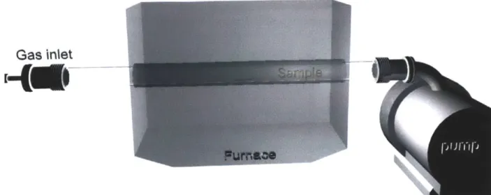
Gas inlet
Figure 5 Schematic of the CVD setup used for graphene growth
Graphene was synthesized as previously reported'6 using copper as the catalyst material.
Briefly, under low pressure (400mTorr) a piece of copper foil (Alfa 13382) was annealed in a gas flow of 10 standard cubic centimeters (secm) hydrogen at 10000 C for 30 minutes before 20sccm methane gas was introduced to initiate the graphene growth. To control the graphene growth rate, 50sccm of hydrogen flow was used during the growth period. After the synthesis process was completed the material was cooled down under 5sccm hydrogen to prevent oxidation and to minimize hydrogenation reactions of the graphene.
1.3.2 Graphene Transfer
One issue of the described synthesis of graphene by CVD is the presence of the Cu growth substrate. Since it is metallically conducting, Cu will short out electronic devices fabricated on the grown graphene. Effort is being directed to circumventing this problem
however, means that higher energy barriers have to be overcome and the necessary growth temperature is incompatible with many substrates and applications.
Until the issue of energy efficient graphene synthesis on dielectric substrates can be overcome, a transfer step is required to move the graphene from the growth substrate to a target substrate".
The transfer process used here has the following steps:
e Immobilization of the Cu-foil on a PET substrate by taping of the edges
e Spin-coating of 9% Polymethylmethacrylate (PMMA)in Anisole solvent at
2500rpm on the graphene covered Cu substrate
* Hard baking of the sample at 120'C for 10 minutes
e Removal of the plastic backing
* Removal of Cu-foil by exposure to Transene CE 100 copper etchant
* transfer of the floating PMMA/graphene membrane into water
e Positioning of the membrane onto a target substrate
* Removal of the PMMA supporting layer by annealing in Ar/H2 forming gas.
1.3.3 Atomic layer deposition
Atomic layer deposition (ALD) is a process that can deposit high quality thin films. Due to the self-limiting nature of the deposition process, monolayer thickness resolution can be achieved.
The deposition process consists of the sequential exposure of a sample to two materials First, a precursor is introduced that physisorbs onto the surface. The subsequent exposure to a reactant changes the chemical makeup of the precursor thus forming a stable
compound. The exposure cycle can than be repeated to add subsequent layers of material onto the grown ones.
In the presented work trimethylaluminum (TMA, A12(CH3)6) was used as the precursor
and water as the reactant. In this system TMA reacts with surface hydroxyl groups under methane formation. This reaction proceeds until the surface hydroxyl groups are
passivated and because TMA does not react with itself it is self limiting. In a second cycle water is introduced that reacts with the TMA to form Aluminum oxide with hydroxyl groups under methane production. These hydroxyl groups form the foundation for subsequent cycles'8.
To achieve deposition of monolayer films purging under inert gasses and elevated temperatures are used to remove excess precursor.
pressure gauge
Figure 6 Schematic of homebuilt ALD system in the nmelab
A homebuilt ALD system is available in the nanomaterials and -electronics group of Prof.
Kong (as shown in Figure 6). Both, precursor and reactant were dosed by Swagelok high speed ALD valves (6LVV-ALD3G333P-CV) in 15ms pulses. The system was held at
125'C at a base pressure of 900mTorr and purged for 45s with dry Nitrogen between
cycles. The deposited film thickness was confirmed by AFM measurements on blank Si/SiO2 samples. The deposited thickness per reaction cycle was calculated to be
1.3.4 Analysis techniques
As mentioned previously, the increased interest in graphene coincided with a
breakthrough in its metrology. The following part reviews several tools that were used in this work to elucidate different aspects of graphene properties.
Optical microscopy
The ability to identify mono-atomic variations in thickness of graphene by optical microscopy can be considered one of the most important factors for the success of the mechanical exfoliation method described above.
Through simple optical observation the thickness of obtained graphene flakes could be inferred from their contrast on the sample as seen in Figure 7.
An experienced experimentalist could quickly analyze dozens of flakes within a matter of seconds which permitted locating one micron-sized graphene flake on a centimeter large substrate. The lacking identification ability had made previous attempts to producing graphene prohibitively slow and tedious.
Geim et al.' found that even single layer graphene -as well as other materials- could be distinguished by their contrast on a 300nm Silicon oxide layer grown on a Silicon wafer. The underlying principle of contrast enhancement through multi-beam interference on a dielectric stack was a well known tool to measure the flatness of samples but the strong absorption of a monolayer of graphene results in a large contrast enhancement 2 and has to be considered a fortuitous coincidence.
Figure 7 Optical micrograph of graphene and various thickness multilayer graphene
Atomic force microscopy (AFM)
The operating principle of scanning probe microscopes is based on the voltage induced extension of a piezoelectric material". This allows the scanner head to be positioned by fractions of a nanometer. This unprecedented accuracy in positioning has to be combined with a sensitive feedback scheme. In an AFM a microscopic cantilever is interacting with the sample and its deflection is amplified by a reflected laser beam. The motion of the AFM head is then controlled to minimize the deflection. The necessary travel of the AFM head will thus follow the contour of the sample and return topography information of the
sample. Figure 8 shows a resulting image and height differences can be related to variations in the number of occurring graphene layers.
(b)
z: 30nm
y: 20 pm
x: 20 pm
Figure 8 AFM images of graphene (a) false color representation with estimate of number of layers (b) 3D representation of same image
An estimation of the number of layers can be obtained when considering an interlayer spacing of~0.33nm and a gap between substrate and graphene of-0.7nm, due to the interaction with the substrate and adsorbed water 1. Thus, mono-atomic differences in height can be reliably distinguished through the use of AFM.
Furthermore, changes in the morphology of a sample can be studied by AFM and in the following chapters the occurrence of etch pits is analyzed.
Raman Spectroscopy
Carbon research is one of the most fruitful areas for Raman spectroscopy. As seen in Figure 9, the relative importance of this field to all research on Raman spectroscopy is steadily increasing since the discovery of fullerenes22.
30%
relative # of carbon,graphene,fullerene
related Raman articles
25%
20%15%
10%
5% 0% aMIM 1940 1950 1960 1970 1980 1990 2000 2010 2020Figure 9 Publications for carbon related Raman spectroscopy normalized by total number of all Raman related publications
The reason for this behavior is the immense wealth of knowledge that can be gained by the Raman spectroscopic analysis of carbon systems. In Raman spectroscopy the inelastic
scattering of light most commonly by creation or annihilation of a phonon is analyzed. In a typical graphene spectrum (i.e. Figure 10) several characteristic Raman features can be observed. Momentum conservation limits the number of possible phonons that can be excited through light because photons have a negligible momentum.
The G-band around 1600cm is related to in-plane optical phonons with zero momentum and can be directly excited through optical phonons.
Other Raman modes require a higher order process to satisfy momentum conservation. The G'-band for example is related to a second order process involving the scattering with two optical K-point phonons. Usually such a second order process is much weaker than first order processes but the resonance of the scattered states with the graphene band
G-band peak. Since this enhancement effect is closely related to the G-band structure of graphene, a large G'-band intensity can be considered a fingerprint of graphene. Furthermore, the width of the G'-band is sensitively dependent on changes to the graphene band structure and the perturbation of adding a second interacting layer can thus be detected.
An important feature for the metrology of graphene samples is the D-band around 1350cm-1. It involves the same optical K-point phonon as the G'-band but instead of requiring a second phonon to scatter back to the origin, an inelastic scattering process with a defect satisfies momentum conservation. Thus, the analysis of the D-band intensity
has been widely used as a quantification of the defectiveness of a graphene sample.
Si Si Si
D
G
G*
G'
2D'
4)
0
500
1000 1500 2000 2500 3000 3500
Raman shift [cm-]
Figure 10 Representative Raman spectrum of Graphene and indication of common features
The evaluation of graphene samples solely based on the D/G ratio, however, could be misleading, since details of the phonon-defect scattering process are not well understood. The idea that the D/G ratio is only dependent on defect density would not hold true when comparing samples with different kinds of defects. For example defects terminating in
armchair edges have a small Raman scattering cross section compared to zigzag
terminated defects. Furthermore, resonance effects between defects are expected to affect the collective D-band intensity [D band Raman intensity calculation in armchair edged graphene nanoribbons]. 50 40 30 20 10 0
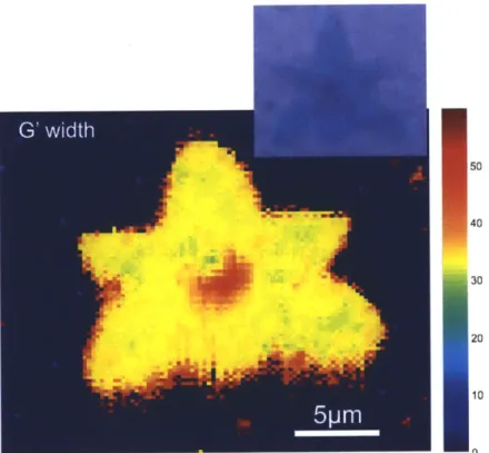
Figure 11 Raman map of the G'-band FWHM of a graphene flake, flake
(inset) optical image of the same
A Raman map can be generated by taking Raman spectra as a function of spatial position.
Thus, the variation of a parameter across a sample can be visualized. An example of these capabilities can be seen in Figure 11 where the full width at half maximum of the G'-band peak is analyzed across a graphene flake. It can be seen that this feature is relatively homogenous across the flake except in the center, where the width increases from
-32cm-1 to ~49cm~'. This area correlates with a darker region in the optical image of the flake (see inset of Figure 11). The larger optical contrast suggests that the center region in
the observed flake consists of bi-layer graphene. The Raman map supports this hypothesis since it is known that interacting bi-layers exhibit a larger G'-band width24
2. A facile tool for the characterization of CVD grown graphene
2.1 Necessity for a new analysis tool
As mentioned in the previous chapter, one common challenge for obtaining high quality samples for many applications is minimizing the density of defect sites in the obtained graphene films. We here focus on the analysis of structural defects in the continuous graphene film because it includes a wide variety of defects, such as lattice defects, incompletely grown graphene, etc. Furthermore these structural defects can degrade the performance of graphene in many respects. For example, Bunch et al.2 found that the presence of a I nm2 opening in a graphene membrane would cause gas effusion that
would drain a graphene sealed microchamber of 1p m3 within one second. Chen et al.26
determined that lattice defects, such as carbon atom vacancies, would deteriorate the electrical transport in a graphene device significantly. Ruiz-Vargaz et al.27 reported a
decrease in the mechanical strength of graphene caused by defects at the grain boundaries. Considerable effort is currently being invested to control the density of structural defects
by optimization of the CVD synthesis process since it is widely believed that this process
step is introducing structural defects. One challenge is to confirm this assumption since other process steps are necessary to prepare the graphene for analysis: To analyze graphene by high resolution transmission electron microscopy, for example, the material has to be transferred to grids or membranes28. The quality of Raman spectroscopy suffers under a low achievable signal-to-noise ratio when done on metallic substrates.
Thus, a transfer step is normally necessary before the analysis can proceed. This transfer step itself can introduce defects through tearing, exposure to acids, residues, etc2 9. Thus, a high resolution analysis technique is needed that does not rely on a transfer step.
Another issue is the comparison of results obtained by different synthesis protocols and
by different groups. The restricted availability of current metrology instruments that can
analyze openings in the grown graphene sheet and the complexity of the necessary measurements limit their practical applicability. Thus, there is a need for a broadly available and scalable metrology tool.
A final requirement for a broadly appealing graphene analysis technique would be speed
and ease of use of the process. Currently, scanning probe techniques as well as scanning spectroscopy techniques are relatively slow and can only give feedback about the quality of small graphene regions.
2.2 Concept of graphene passivated etching
We will here introduce an analysis technique that can overcome these issues and has the potential to become a useful graphene metrology tool. The method uses materials and tools that are widely available and is compatible with a multitude of imaging techniques. It can furthermore be applied directly to as-grown samples without the need for a transfer step. The sensitivity of the described technique can be tuned finely to visualize openings in the graphene film originating from incomplete growth as well as lattice defects by graphene passivated copper etching. A correlation was found between structural defects and the maximum mobility of graphene devices which emphasizes the usefulness of the described analysis technique.
The analysis technique relies on the analysis of the etching behavior of graphene passivated copper substrate when exposed to copper etchant.
Graphene was synthesized on copper foil as detailed earlier and a small piece of the sample was then affixed to a glass slide with double sided tape to simplify handling. A drop of commercial copper etchant (Transene APS- 100) was deposited onto the graphene sample with a pipette (This ammonium persulfate-based etchant was chosen over FeCl3 based etchants because this etchant did not leave residues on the sample). After waiting for 10 seconds, the drop of etchant was removed by thorough rinsing with deionized water and subsequent blow-drying with compressed nitrogen.
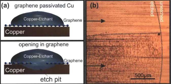
The basic concept of the proposed analysis tool is described in Figure 12(a): Regions on the copper substrate covered by graphene are protected from being corroded whereas regions without a graphene layer are readily attacked by the copper etchant.
2.3 Experimental results
This concept is validated by the comparison of the left and the right area of Figure 12(b). In the top area of the image a graphene layer deposited by chemical vapor deposition protected the Cu substrate while in the lower area the graphene was partially peeled off using a Scotch tape. Both sides were exposed to copper etchant following the described procedure but a significant difference in morphology can be seen. Simple visual
inspection reveals a larger roughness of the copper substrate on the lower side. This indicates that graphene effectively passivated the upper area as suggested by Chen et al.30
This ability to easily confirm the presence of graphene after growth already represents a significant advantage over existing analysis techniques. With commonly used analysis tools such as optical microscopy or Atomic Force Microscopy (AFM) answering this fundamental question requires the transfer of the graphene from the growth substrate to a different target substrate - a process that is both time consuming and might compromise
the results since the graphene film can get damaged or contaminated in the transfer process. The process is both easy and time effective and takes between 1-5minutes.
(a)
graphene passivated Cu
Copper-Etchant
C
ope igi gahn
Cop)per-Etchanit Qah
Copper
Figure 12 Schematic of the graphene passivated etching process: In the case of complete graphene coverage (upper panel) no etching occurs but openings in the graphene film result in etch pits in the copper substrate (lower panel). (b) Optical micrograph of copper surface after 10s etching with complete (top) and partial (bottom) graphene passivation layer
The power of the described analysis technique lies in the ability to visualize structural defects in the graphene film through analysis of the etch patterns in the Cu substrate. Since the graphene is expected to protect the Cu substrate, no etching should occur on the graphene passivated Cu substrate.
There could be different reasons for the observed etching. For example the graphene could be destroyed by the Cu etchant and these openings could be permeated to generate etch pits. This hypothesis can be discounted because the ammonium persulfate based copper etchant is only a mild oxidant and is not expected to attack the carbon-carbon bonds in the graphene sheet. In single walled carbon nanotubes this etchant was shown to
introduce defects in the nanotube wall only upon several hours of exposure and
agitation3 and the observed SWNT cutting proceeded by enlarging existing defects32.
The resistance of graphene to ammonium persulfate was also confirmed by etch tests on graphite where no etching was observed even after prolonged exposure (30 hours). Thus, graphene is expected to protect the underlying copper from oxidizers (as demonstrated by Chen et al.30). This is the reason for routinely destroying the graphene on the back of the catalyst foil before transfer to ensure fast etching of the copper substrate.'6
Another reason could be the permeation of copper etchant through existing structural defects in the graphene film (as indicated in Figure 12(b)). These structural defects could originate from several different scenarios:
e Incomplete graphene growth results in only partial coverage of the substrate
starting from nucleation points that form flakes as observed by Li et al.(Li, Magnuson et al. 2010)
e Particles on the catalyst surface represent obstacles that cannot be covered by graphene and when removed leave exposed copper substrate.
" Lattice defects present openings in the continuous graphene film that could be
permeated by the etchant.
We subsequently demonstrate the ability to identify those different structural defects by the described analysis technique and study its sensitivity.
2.4 Quantification of graphene defectiveness
Figure 13 shows a comparison of the morphology of different samples after exposure to copper etchant. Figure 13(a,d) represents a copper substrate that had only been annealed
and no graphene growth was initiated. Thus, the copper substrate was not passivated with graphene and uniform etching occurred across the sample, apart from some impurities. The morphology in Figure 13(b,c) was obtained after 10 minute exposure to a low partial pressure of methane (3sccm). As reported by Li et al.3 these conditions do not result in a continuous film of graphene. Instead, only individual flakes of graphene grow. The effect of those flakes protecting certain areas of copper substrate from the etchant can be
distinguished both in the optical micrographs (Figure 13(b)) and in the atomic force microscope images (Figure 13(e)). Finally, the completely grown graphene film will protect the copper as seen in Figure 13(c,f). The holes represent defects in this continuous graphene film that are permeated by copper etchant. These defects are caused by
impurities in the copper foil and lattice defects, as described below.
To quantify these observations we define a parameter 0 that is proportional to the surface coverage of graphene. The parameter is determined as the ratio of unetched copper substrate to total area. The parameter is obtained by analyzing the projected area of the etch pits identified in AFM images and normalizing the projected area to the overall AFM image size. As expected, 0 of unprotected copper substrate is low (1%), increases to 30% for incomplete graphene growth and reaches 95% for completely grown graphene. It has to be noted that 0 corresponds to the graphene coverage only for vanishing etching time since under-etching of the graphene can occur. Thus, care has to be taken in the comparison of 0 obtained by other methods (i.e. through the analysis of scanning electron micrographs) with the described technique since the graphene coverage is underestimated
by this technique. The under-etching, however, presents the opportunity of varying the
etching times or low etchant concentrations- large openings, caused for example by incomplete growth, can be discerned. High etchant exposures, on the other hand, will result in the amplification of small openings such as lattice defects. Thus, at longer etching times defects can be made visible that are normally not discernible in SEM or even AFM images. Through this behavior, the analysis of atomic imperfections through broadly available imaging tools, such as optical microscopes, can be envisioned.
Figure 13 Morphology after 10s etching for 3 different growth conditions by optical microscope (a-c) and AFM(d-f) images: (ad) no graphene growth (0=1%) (be) incomplete graphene film (0=30%), (c,f) complete graphene film with a low density of openings (0=95%)
2.5
Information about the substrate
The etching patterns can furthermore reveal the crystallographic orientation of the copper substrate. Figure 14 shows a graphene passivated copper sample with a large density of etch pits of triangular shape. This observation is illustrated by investigation of a single
etch pit in Figure 14(c). The anisotropic etching behavior was already observed in 1962 34
and subsequently attributed to the preferential etching of the Cu (100) crystallographic
planes .
The parallel alignment of the etch pit boundaries over large areas is supported by the occurrence of distinct symmetric lines in the spatial Fourier transform (Figure 14(d)) of a
50x5Oum area. This 2D FFT pattern indicates the high number of similar spatial
frequencies occurring corresponding to parallel edges with the same slope. The observed large scale crystallographic orientation indicates the large single crystalline domains in the copper foil. The SEM image in Figure 14(e) shows that transitions between single
crystal domains can be identified by the difference in orientation of the etch pits. The occurrence of faceted etch pits was reported to be sensitively dependent on the etchant or the copper quality3 4 36. We have only observed faceting during the initial studies and hypothesize that the batch-to-batch variation of the purchased Cu foil or the aging of the etchant could be responsible for the subsequent random shapes of the etch pits.
b
Figure 14 (a) AFM image of aligned etch pits, (b) orientation of crystallographic planes (c) 3D representation of AFM close-up of one etch pit, (d) 2D Fourier transform of (a), (e) SEM image of two areas with different shaped etch pits
2.6 Comparison to Raman spectroscopy
To test the sensitivity of the new analysis tool, samples with a variety of defect densities are necessary. This variation in defects was achieved by intentionally introducing more defects in an as-grown sample and analyzing the variation in the etch pit morphology. Ozone generated by UV-illumination has been shown to create lattice defects37 by
oxidizing carbon atoms. The changes in graphene quality after exposure of graphene to UV-ozone in a UVO-cleaner (Jelight Company) were measured by analyzing 0 for various UV-ozone exposure times tuv after 1 Os of copper etching and by Raman
spectroscopy of a similar graphene sample transferred onto silicon substrates with 300nm SiO2
-(a) (b) 100 0.9 Pniare 0.8 3., -7ozn 180s 95 00.7 o 90 .0.
iJ
120s '5 85 * ~0. 5 S85 10. 1200 .1600 2000 2400 2800 3200 0 -03Raman shift (cm1)I 80 0.2 Os 3s90S C 75 70. 70 0 1 60s 0 50 100 150 200 100 95 90 85 80 75UV exposure time ta,, [s] unetched area 0[%
Figure 15 (a) Unetched area 0 as a function of UV-ozone exposure, (b) comparison of Raman 'D/'G
ratio and 0, (inset) representative Raman spectra at various exposures
Figure 15(a) shows that 0 decreases for longer exposures to ozone. This agrees with the prediction that more lattice defects are generated that allow permeation of copper etchant
and thus a higher density of etch pits are formed. A more detailed analysis of the plot of with exposure time tu reveals information about the defect density introduced by ozone. At low ozone exposures the lattice defects are individually and randomly distributed across the samples and thus each defect results in one hole in the graphene film. In the high defect density regime, on the other hand, the addition of another defect would only
enlarge existing holes. Because of the described under-etching, several individual holes will have a larger effect on the etched area than one large hole. Thus the transition between the low and high defect density region would result in a decrease of the slope of O(tuv) . From the linear decrease in O(tuv) it is inferred that all measurements are
performed in the low defect density regime.
The inset of Figure 15(b) shows representative Raman spectra of the same graphene sample, transferred to an Si/SiO2 wafer, for different tuv. A strong variation of the D-band region around 1 300cm-1 can be observed. This feature originates from a K-point
phonon and since elastic scattering with a defect is necessary to maintain momentum conservation, the D-band intensity is a widely accepted way of quantifying the defect density of nanotubes and graphene". Additionally, the second-order Raman features of the G' and G+D exhibit large variations upon increased defect concentration as shown by Alzina et al.38.
The defect density, as quantified by the peak intensity ratio of the D-band to the G-band feature (ID/IG), was correlated with 0 at different exposure times tuv in Figure 15(b).
It can be seen in Figure 15(b) that the ID/G ratio does not change within the first 90 seconds of UV ozone exposure, while 0 measured by etching changes monotonically. This indicates a limited sensitivity of the Raman ID/G ratio to defects generated by ozone. This observation can be explained by the fact that the Raman signal of the D-band is proportional to the sum of the Raman signal coming from all of the defects within the
laser spot and was found to be determined by - D ( ) (where EL=2.33eV is
IG 7.3 x10 9 -EL
the excitation energy in our experiments)39. Thus the minimum observable defect density as determined by the intensity contrast between the G-band and D-band is determined by noise, electronic amplification and background signal and cannot be smaller than 1 defect/(lum)2. This detection limit could be insufficient for certain applications since it is shown subsequently that the electric properties of graphene devices might be sensitive to variations below this limit.
The analysis of etch patterns, on the other hand, has no such limitation to the minimum defect density. There is furthermore no theoretical limit for the minimum defect size.
defects would be visualized by the etching procedure. Previous studies on the cutting of single-walled nanotubes have shown that the use ammonium persulfate etchant will exploit lattice defects and initiate an oxidation process starting at these lattice defect points. Thus, for high enough etchant exposure lattice defects would be widened and permeation of etchant through the film would amplify the defects. Experiments with higher quality graphene have to reveal if this ultimate sensitivity can be reached, since the current graphene is exhibiting too many larger openings that normally overwhelm the response from lattice defects.
Aside from its demonstrated high sensitivity, the graphene passivated etch analysis tool is selective only to openings in the graphene film and not to other kinds of imperfections
such as PMMA residue or amorphous carbon, which, for example, would also contribute to the Raman D-band intensity 40.
2.7 Effect of defects on electrical transport
Finally, the impact of structural imperfections on the application of graphene is
investigated. The electrical transport characteristics of ~60 graphene samples grown at different growth parameters were correlated with their defectiveness as quantified by 9. For this experiment, the sheet resistance and carrier mobility were extracted over an
8x8mm2 graphene area from 4 probe measurements in van-der-Pauw geometry. As expected, there is a wide variation of mobilities and sheet resistances that are thought to be caused by growth induced differences in the quality of the graphene films, i.e. through
26
2500
1000
2000
150>
15000
0
500
S
E1000
-500-E
E A CU U) E l0
80
85
90
95
100
avg unetched area 0
Figure 16 (a) Maximum mobility and corresponding sheet resistance for devices within an interval of graphene coverage. The insets show representative AFM images after 5s etch of graphene devices corresponding to the low and high mobility cases (scale 20x2OIm2)
Figure 16 plots the highest mobilities obtained from samples that exhibit an average 0
within a certain range. The range of 0 was chosen to be 4% which is the average error of the measured 0 within a sample caused by inhomogeneity across the macroscopic
graphene film.
A clear trend can be seen for mobility and the corresponding sheet resistance of samples
as a function of average 0.
The increase in mobility with increasing 0 leads us to the following explanation: Graphene mobility is determined by different factors, for example charged impurity scattering and electron-electron interaction caused by high doping and structural defects26.
According to Mathiesen's rule the process with the shortest scattering time or lowest mobility limits the overall mobility of the device. In the case of high mobility devices, charged impurity scattering and electron-electron interaction are low enough that
scattering on lattice defects and openings determines the limit of the carrier mobility.
The increase in sheet resistance for decreasing 0 can be explained by the less efficient transport of carriers in the presence of structural defects through scattering and confirms the previous explanation for decreased carrier mobility.
The finding that the maximum achievable mobility is determined by the presence of structural defects emphasizes the need for optimization of graphene growth and proves the value of the described analysis technique.
2.8 Challenges of the analysis technique
The described analysis technique can be destructive under certain circumstances: It was found that graphene would tear around the etch pits during a subsequent transfer process as shown in Figure 17(a). There are three situations when the tearing could occur:
" The graphene could be weakened through introduction of defects during the
copper etching process. This option can be ruled out because of the proven resistance of graphene to the etchant. Furthermore Figure 17(b) demonstrates that the Raman spectra obtained from graphene transferred from unetched and etched Cu substrates are indistinguishable.
e The graphene could tear during the drying process when capillary forces due to
the evaporating liquid could pull the graphene membrane into the etch pit.
b
- etched unetched
3000
Figure 17 (a) Optical micrograph of graphene transferred from the etched and unetched parts of a copper substrate, (b) Raman spectra of etched and unetched graphene areas showing identical results
Defect-free graphene, on the other hand, would not exhibit underetching and the
subsequent transfer process would not result in tears. Thus, the analysis technique is only destructive in the case of defective graphene, a material that would not warrant transfer anyways.
2.9 Summary
The process of graphene passivated copper etching described here could provide a simple metrology tool for the optimization of graphene synthesis. It can be routinely used to assess graphene surface coverage and continuity which makes this well suited for in-line quality control in industrial scale graphene fabrication processes.
In addition to its anticipated wide application in future graphene synthesis optimization, the described tool lends itself to the analysis of other CVD synthesized thin film materials, such as Boron Nitride4 or BCN42, which, due to their insulating character, limited light
absorption, etc., cannot be easily investigated with traditional metrology tools. Finally, the availability of the necessary materials and the flexibility of using many different imaging techniques make the graphene passivated etching approach well suited for comparing the results from different research groups and will be hopefully added to the metrology tool kit.