HAL Id: hal-01706842
https://hal.archives-ouvertes.fr/hal-01706842
Submitted on 12 Feb 2018
HAL is a multi-disciplinary open access archive for the deposit and dissemination of sci-entific research documents, whether they are pub-lished or not. The documents may come from teaching and research institutions in France or abroad, or from public or private research centers.
L’archive ouverte pluridisciplinaire HAL, est destinée au dépôt et à la diffusion de documents scientifiques de niveau recherche, publiés ou non, émanant des établissements d’enseignement et de recherche français ou étrangers, des laboratoires publics ou privés.
Study of the composition of hydrogenated silicon nitride
SiNx:H for efficient surface and bulk passivation of
silicon
J.-F. Lelièvre, E. Fourmond, A. Kaminski, Olivier Palais, D. Ballutaud, M.
Lemiti
To cite this version:
J.-F. Lelièvre, E. Fourmond, A. Kaminski, Olivier Palais, D. Ballutaud, et al.. Study of the composition of hydrogenated silicon nitride SiNx:H for efficient surface and bulk passiva-tion of silicon. Solar Energy Materials and Solar Cells, Elsevier, 2009, 93 (8), pp.1281 - 1289. �10.1016/j.solmat.2009.01.023�. �hal-01706842�
1
Study of the composition of hydrogenated silicon nitride SiNx:H
for efficient surface and bulk passivation of silicon
J-F Lelièvre1*, E. Fourmond1, A. Kaminski1, O. Palais2, D. Ballutaud3 and M. Lemiti1
1
Institut des Nanotechnologies de Lyon (INL-INSA), UMR CNRS 5270, INSA de Lyon, Bât Blaise Pascal, 7 avenue Jean Capelle, 69621 Villeurbanne Cedex, France
2 TECSEN, UMR CNRS 6122, Université Paul Cézanne-Aix-Marseille III, 13397 Marseille Cedex 20, France 3 GeMAC, 1 place Aristide Briand, 92195 Meudon Cedex, France
Abstract:
This work is a contribution towards the understanding of surface and bulk passivation provided by hydrogenated silicon nitride, giving emphasis to SiNx:H chemical structure and hydrogen desorption mechanism. Considering the deposition system used (Low Frequency PECVD), we report very low values of surface recombination velocity Seff. As-deposited Si-rich SiNx:H leads to the best results (n-type: Seff = 4 cm/s – p-type: Seff = 14 cm/s). If field-effect passivation is always high whatever the SiNx:H stoichiometry, it appears that the interface state density Dit is the key-parameter when considering surface passivation provided by SiNx:H layers of different stoichiometries. After annealing, the surface passivation quality is drastically deteriorated for Si-rich SiNx:H whereas it is lightly improved for low refractive index SiNx:H (n ~ 2 – 2.1). The chemical analysis of the layers highlighted a high hydrogen concentration, whatever the SiNx:H stoichiometry. However, the H-bond types involved as well as the hydrogen desorption kinetics are strongly dependent on the SiNx:H composition. Furthermore, “N-rich” SiNx:H appears to be denser and thermally more stable than Si-rich SiNx:H. Such a SiNx:H layer is believed to induce the release of hydrogen in its atomic form, which would diffuse towards the substrate assisted by defects situated at the surface and in the bulk of the silicon substrate. Consequently, this would induce the minimisation of the Dit and the increase of the bulk lifetime τb after a high temperature step. On the other hand, Si-rich SiNx:H (less dense and thermally less stable) would lead to molecular hydrogen desorption into the ambient. Moreover, a high fraction of Si-H bonds formed at the SiNx:H/Si interface during the SiNx:H deposition would be broken by the high temperature process, increasing Dit and therefore Seff. The results are discussed and compared with the literature data reported for the different forms of PECVD reactors.
Keywords : Silicon Nitride, PECVD, passivation, solar cells
1. Introduction
During the industrial silicon solar cell fabrication process, the deposition of a thin a layer of hydrogenated silicon nitride SiNx:H (abbreviated to SiN in the following) on the silicon substrate is of crucial importance. Indeed, the SiN layer acts as antireflective coating (ARC) and thus reduces considerably the optical losses [1]. Furthermore, its chemical composition, and particularly its high hydrogen content, leads to remarkable properties that allow to passivate (neutralize) defects situated at the surface and in the bulk of the silicon substrate,
* Corresponding author: Presently at the Instituto de Energía Solar, Avd. Complutense s/n, 28040 Madrid (Spain) – email: [email protected] – Tel: +34 - 91 45 33 555 – Fax: +34 - 91 54 46 341
2
especially when considering multicrystalline samples (mc-Si) [1, 2, 3, 4]. Thanks to this single fabrication step, the solar cell efficiency is strongly increased. However, the origins of these interesting properties are still subjected to discussions, which is reinforced by the fact that a wide variety of SiN deposition systems are available.
In the photovoltaic area, SiN is currently deposited by Plasma-Enhanced Chemical Vapour Deposition (PECVD). As most of the photovoltaic research centres employ microwave (µW) remote or high frequency (HF) direct PECVD reactors, very few results are published on the passivation properties of SiN elaborated by low frequency (LF) direct PECVD systems. The two first kind of reactor are known to provide a better surface passivation than the last one as the silicon substrate is not subjected to ion bombardment during deposition [5]. However, LF-PECVD reactors are widely used in the industrial sector and some authors have reported that they lead to a more efficient hydrogenation of the silicon substrate [6, 7]. Indeed, the hydrogen contained in the SiN layer is known to be the origin of defect neutralization deep in the bulk of the silicon substrate, after the rapid high temperature annealing used for the industrial co-firing of the metallic contacts [1]. The atomic hydrogen (H) diffusion from the SiN layer into the Si substrate would be governed by defect trapping mechanisms and would therefore have more effect on “bad” quality substrates (such as mc-Si) [4]. Furthermore, Sopori et al. [6] suggested that the damage induced by ion bombardment during LF-PECVD deposition would induce surface traps (Process Induced Traps – PITs) that would “stock” hydrogen and then redistribute it during annealing, resulting in an efficient bulk passivation. However, other authors have highlighted the important role of SiN density on the bulk passivation process [8]. A high density SiN would release less hydrogen than a material of lower density, but this key-element would diffuse in its atomic form, which is desirable for bulk passivation [9].
Another important aspect of SiN is its surface passivation properties. Indeed, the silicon surface presents a high density of dangling bonds, which is correlated to high recombination rates. The density and distribution of states introduced by these defects in the Si bandgap are expressed by the interface state density Dit. The Schokley-Read-Hall (SRH) recombination mechanism formalism can be reformulated in this case, considering recombination rates Us by surface unit [10]:
(
)
( )
( )
( )
∫
+ + + − = C V E E it n s p s i s s th S D E dE E p p E n n n p n v Uσ
σ
1 1 2 (1)where ni is the intrinsic electron density, vth is the thermal velocity of charge carriers and ns and ps are surface electron and hole concentrations, respectively. σn and σp represent the capture cross-sections of the considered defect for electron and holes, respectively. n1 (respectively p1) is defined as the electron (hole) density in the conduction band EC (valence band EV) when the Fermi level EF coincide with the considered energy level E. Surface recombination velocity S is used to quantify these recombination rates and is defined as:
∆
= S
S S. n
U (2)
where ∆ns is the concentration of carriers injected in the vicinity of the surface. Experimental results usually refer to effective surface recombination velocity Seff, obtained by subtracting the volume contribution from the measured total sample lifetime τeff [11].
SiN exhibits the two fundamental mechanisms that can contribute to minimize the recombination processes at the silicon surface [1, 3]. First, the deposition of such a layer
3
induces the passivation of Si dangling bonds at the substrate surface and hence the reduction of the interface state density Dit. On the other hand, the high positive fixed charge density Qf reported for SiN allows reducing minority carrier concentration at the surface (hence ns or ps) thanks to field-effect passivation [3, 12]. Indeed, a high density of positive fixed charges can induce an accumulation layer (respectively an inversion layer) at the surface of a moderately doped n-type (p-type) silicon substrate, which hence would repel the minority carriers from this high recombination region. In both cases, the silicon energy band bending induced by these charges leads to a strong reduction of the surface recombination velocity1. The Seff values reported, which were gathered by Cuevas et al. [11], are very low, indicating that SiN can provide better surface passivation properties than thermal SiO2 for moderately doped silicon [13, 14]. Here again, the SiN density appears to have a great influence on the passivation of the Si surface, before and after the co-firing step. Weeber et al. [15] reported that as-deposited Si-rich SiN provides the best surface passivation while after the high temperature step, N-rich (low refractive index) SiN leads to the best results. As the mass density has been identified as a decreasing function of the Si-content [16, 17], this parameter has become of great interest. It was also verified that a direct correlation exists between film mass density and Si-N bond concentration (which can be determined by FTIR measurements) [18]. Different studies showed that a low refractive index SiN layer (n ~ 2) with an optimum Si-N bond density between 6-8×10²² and 1.3×1023 cm-3 provides the optimal surface (and bulk) passivation after the firing step [19, 20, 21]. If these results are convincing, it is obvious that the temperature profile used will have also an important impact on the final passivation properties [21]. In addition, the deposition system and parameters may have an influence on these properties.
For SiN layers deposited by Low Frequency PECVD, the work presented here comforts the central role of the film mass density observed for other configurations of PEVD reactors. Furthermore, thanks to the structural and chemical characterizations of the SiN films, we will give emphasis to the hydrogen desorption process and its consequences on defect passivation. Different SiN stoichiometries were deposited thanks to a direct LF-PECVD reactor prototype (SEMCO-Engineering). In order to understand deeply the surface and bulk passivation properties of such SiN, we will first look closely at the SiN chemical structure, the hydrogen content and its desorption mechanism thanks to various characterization techniques. Then, we will present the results of the Capacitance-Voltage (C-V) measurements from which we could determine the densities Qf and Dit. Thanks to minority carrier lifetime measurements, we will subsequently demonstrate the good surface passivation properties provided by the SiN deposited with such a reactor. We will discuss on the origins of the passivation quality before and after a high temperature step. Finally, we will examine the bulk passivation process following such an annealing.
2. Experimental
After a standard cleaning of the silicon substrates, the SiN layers were deposited by direct LF-PECVD (440 kHz – SEMCO-Engineering). Only the SiN stoichiometry was modified, adjusting the ammonia-to-silane gas flow ratio R = NH3/SiH4 while the temperature (T = 370°C) and all the deposition parameters (pressure, plasma power, total gas flow) were maintained constant. For each stoichiometry, several samples were elaborated at the same time in order to be characterized by the various techniques used in this study.
For all the samples, the thickness, wavelength-dependant refractive index n(λ) and
1 Note that S
eff, defined by an effective surface at the limit of the quasi-neutral region, takes into account the recombination taking place at the surface as well as in the vicinity of the surface [11]
4
extinction coefficient k(λ) of the different SiN films were deduced by spectroscopic ellipsometry (JobinYvon UVISEL), using Tauc-Lorenz dispersion model [22]. The refractive index n at λ = 605 nm will be used through this work to estimate the stoichiometry of the different SiN layers.
The influence of Rapid Thermal Annealing (RTA-ADDAX R1000) was systematically studied in order to simulate the co-firing of solar cell contacts. For this purpose, the samples were annealed at around 800°C during one second. The temperature profile was determined thanks to Transmission Line Model (TLM) measurements [23]: screen printing of industrial Ag paste was applied on standard ARC SiN/Si samples and the RTA parameters were adjusted for optimal contact resistance.
a. XPS, SIMS, FTIR and TPD measurements
The chemical composition x = [N]/[Si] of the films was evaluated by X-photoelectron spectroscopy (XPS), carried out on the surface of five SiN (R = NH3/SiH4 = 2; 3.5; 4.5; 7.7; 10) deposited on p-type CZ c-Si substrates (ρ = 10 Ω.cm – NA = 1.4×1015 cm-3). In order to detect the hydrogen concentration, SIMS measurements were done on the same samples. In parallel, FTIR measurements were performed in the transmission mode to investigate the evolution of Si-H, N-H and Si-N bond densities according to the stoichiometry of various SiN (R = 2; 3.5; 4.5; 7.7; 10; 15; 30) deposited on double-side polished 10 Ω.cm p-type CZ c-Si. The effect of the RTA process on the H-content and H-bonds in the SiN films was also studied using samples elaborated at the same time and subsequently annealed. Finally, Temperature Programmed Desorption (TPD) measurements were carried out on three SiN samples (R = 2; 7.7; 10) to investigate the temperature dependence of hydrogen releasing. In a vacuum environment, a temperature ramp was applied to the sample (20°C/min from 20 to 810°C) and a mass spectrometer allowed detecting the gas flow of molecular hydrogen H2 released from the SiN layer.
b. C-V measurements
In parallel, the electrical characteristics of SiN layers were obtained by dark capacitance-voltage (CV) measurements at different frequencies (1, 10, 100 kHz and 1 MHz using a HP4284A) performed on metal-insulator-semiconductor (MIS) structures: Al/SiN/Si/Al. For this purpose, single-sided SiN layers were deposited on 10 Ω.cm p-type CZ c-Si wafers (R = 2; 3; 3.5; 6; 7.7; 10). Two CZ c-Si wafers were placed in the reactor for each run, one of which was RTA annealed before the deposition of aluminium by electron-beam evaporation on both sides of the structures. The MIS samples were then annealed at 400°C for 15 minutes under H2 in order to obtain ohmic contacts. The CV measurements were performed with applied voltages swept between the inversion and the accumulation modes and back to the inversion. They allowed determining the fixed charge density Qf in the SiN layer thanks to both the computation of the flat-band capacitance CFB and the Maserjian and Vincent method [24]. For some of the samples, the interface state density Dit could also be determined using the combined high-low frequency method [24]. However, due to hysteresis and leak effects, this computation was difficult and we prefer to present only the few unambiguously obtained values.
c. Lifetime measurements
For lifetime measurements, SiN layers were deposited by direct LF-PECVD (R = 2; 2.5; 3.5; 6; 7.7; 10) on both surfaces of 5Ω.cm p-type and n-type FZ c-Si wafers as well as on
5
textured 2.5 Ω.cm p-type mc-Si substrates. The mc-Si samples were taken from consecutive wafers from the same ingot and present the same grain distribution, from which we can suppose an equal distribution of initial bulk lifetime τb. Lifetime measurements were carried out using the PhotoConductance Decay (PCD) method developed by Sinton and Cuevas [25], in both the transient and quasi-steady state measurement modes. Under the assumption that all studied FZ c-Si samples have equally high values for the bulk lifetime (τb), the extracted values of the effective lifetime (τeff) can be used as a measure of the surface passivation quality of the different SiN layers. Indeed, if we consider a uniform carrier generation in the silicon wafer (∆n = ∆ns), effective lifetime can be expressed as [26]:
W Seff b eff 2 1 1 ≈ +
τ
τ
(3)The usual hypotheses made on τb lead to generally overestimated values of Seff. This simplified equation can be used with an error < 4% for Seff lower than 250 cm/s for such c-Si substrates [27].
The results were confirmed independently by the microwave phase-shift (µW-PS) technique [28], giving Seff and τb cartographies of the studied samples. The latter values were found with a 200 µm spatial resolution and for an injection level ∆n of 7×1014 cm-3. Such a value allows working at low injection level while avoiding measurement artefacts induced by material defect (especially when considering mc-Si substrates) [29]. Furthermore, such ∆n is equivalent to the carrier photogeneration under standard AM1.5G illumination in an ordinary silicon substrate of thickness W = 300 µm and mean lifetime τ = 80 µs [26]. Hence, τeff results are given in this work for this ∆n = 7.1014 cm-3, although they do not correspond to the highest values. All the samples were then annealed and lifetime measurements were performed again.
3. SiN Stoichiometry and hydrogen desorption
a. SiN stoichiometry
For two of the samples studied by XPS (R = 2; 7.7), the chemical composition of the SiN coatings was determined along the full thickness of the films thanks to layer abrasion. This showed a stable x = [N]/[Si] ratio through the whole width of the SiN layers, which indicates a good SiN structural homogeneity. These measurements demonstrated as well that a thin layer of silicon oxynitride SiOxNy (< 2 nm) is formed at the SiN/Si interface, which is due to silicon oxidation during sample loading into the PECVD reactor.
The x ratio was evaluated 5 nm deep in the different SiN layers, giving x = 0.35; 0.49; 0.59; 0.78 and 0.81 for the films obtained with a gas flow ratio of R = 2; 3.5; 4.5; 7.7 and 10, respectively. As expected, the silicon content decreases as the gas flow ratio is increased. However, these results indicate a high silicon excess for all the SiN layers. It is worth noting here that the SiN film obtained for R = 7.7 has a refractive index n(605nm) = 2.03 close to that of stoichiometric Si3N4 (n[605nm] = 2.04 [30]), for which x = 1.33. The difference between the [N]/[Si] ratio and the optical properties is believed to be due to hydrogen and void incorporation in the PECVD films, which produces a variation of the optical constants. This could be attributed to the low frequency plasma process, as it has been already observed [31, 32]: the composition of the SiN films remains far from the stoichiometry (x = 1.33). The dissociation and activation of the reactive species issued from ammonia needs much more energy than for the silane radicals [33, 34]. For the deposition temperatures considered, and
6
since low frequency is used for plasma excitation, the NH3 reactive species density is believed to stay low in spite of the increasing of the NH3 gas flow.
With the deposition conditions used in this work, it seems difficult to obtain x values greater than 0.9. However, the large silicon excess produced during the plasma process gives rise to interesting layer properties for such low refractive SiN: indeed, we have previously demonstrated the intrinsic formation of silicon nanocrystals (nc-Si) in the amorphous SiN matrix for a tight range of SiN stoichiometries (0.7 < x < 0.9) [35, 36]. These nanostructures (ns-Si) could be useful for the development of all-silicon tandem solar cells [37]. For the structural composition of the SiN, we thus forward the model proposed by Gritsenko et al. [38] for the chemical structure of their SiN films obtained by Low Pressure CVD. Basically, it considers the formation of ns-Si (in the crystalline form or not) in the SiN matrix which results in a non-uniform compositional distribution. As it was verified with our XPS spectra, as well as with TEM observations [36], this model can be seen as an intermediate solution between the Random Bonding Model (RBM) of H.R. Philipp [39] and the Stoichiometric Statistical Model (SSM) [40]: the matrix would be a mixture of Si and Si3N4 clusters (composed respectively by Si-Si4 and Si-N4 tetrahedrons), separated by a random bonded intermediate SiNy:H matrix. In spite of this atomic-scale heterogeneity, the films are homogeneous in composition within their whole thickness.
It is interesting to link the SiN composition to the refractive index, as the latter is often used as a measure of the Si-content of the layers. The equation proposed by Bustarret et al. [41] gave results very far from the experimental ones. This shows that, in our case, hydrogen and porosity in the SiN layer cannot be neglected. The fact that this equation was successfully used by other authors [12, 20] points out the difference in structural composition for SiN obtained with distinct deposition systems, especially considering the frequency of the plasma excitation. Most of the SiN passivation results published in the literature involve direct high frequency and remote µW PECVD reactors. In these equipments, the Si substrate is not subjected to ion bombardment and an inert gas such as Argon is usually added to the plasma in order to facilitate the NH3 dissociation. This is believed to have a strong impact on the SiN stoichiometry, density and hydrogen content, and subsequently on the optical constants of the material. To link stoichiometry and refractive index, we thus used an empirical relation, inspired from the linear dependence of n and 1/x observed by S. Dauwe [42]:
n = 1.22 + 0.61(1/x) (4)
As expected, this relation is different from the one found by S. Dauwe but it gives a good estimation of the stoichiometry of the SiN deposited with our LF-PECVD reactor (Figure 1). Furthermore, the results we have reported elsewhere [32] with an other LF-PECVD reactor (40 kHz - Centrotherm) are in good agreement with this equation. When comparing SiN obtained with different deposition techniques, the complete complex optical index N = n + ik should be taken into account. Indeed, the extinction coefficient k at low wavelengths gives reliable information on the Si-content of the SiN layer, as we have already suggested elsewhere [43, 44].
b. Hydrogen content
It seems interesting to evaluate the hydrogen content and its evolution according to the SiN stoichiometry. The literature reports H-concentration in the range of ~1022 cm-3, whatever the PECVD reactor configuration used [5, 6, 45], corresponding to 20 to 30 at%. Our SIMS measurements showed good chemical homogeneity and high hydrogen content for all the samples studied. As the chemical structure of the SiN is different from one sample to another,
7
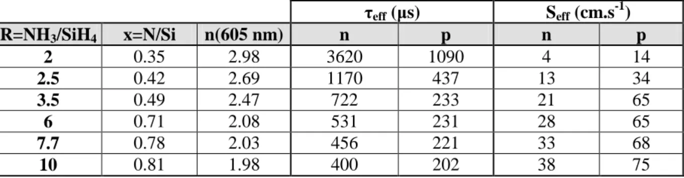
it appears difficult to find a reliable reference for accurate hydrogen concentration determination. However, a relative comparison is still possible: Figure 2 shows the hydrogen spectra for a Si- and a “N-rich” SiN (respectively R = 2 and R = 7.7), adjusting at the same level their respective Si signal (Si28) in the c-Si substrate. The corresponding high hydrogen profiles reveal a really close H-concentration for these distinct materials (n = 2.98 / x = 0.35 and n = 2.03 / x = 0.78 respectively). As it will be discussed below, the relative H-amount in the SiN layer does not appear to be a key parameter for surface and bulk passivation. For this purpose, the study of hydrogen release and diffusion mechanisms gives more valuable information.
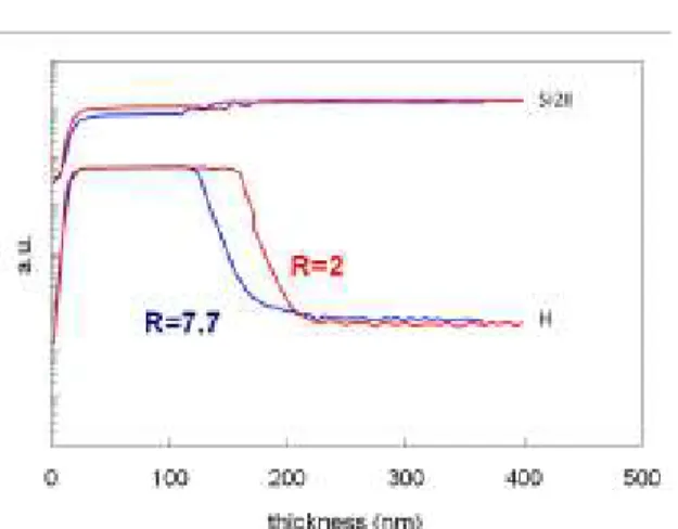
FTIR measurements allow to characterize the bonds involved in the material, and eventually to determine bond densities and thus hydrogen concentration thanks to the method developed by Landford and Rand [16]. We chose not to apply this widely used technique because the employed constants values need first to be calibrated as they seem controversial and dependent on the SiN composition [46]. Nevertheless, these measurements give interesting qualitative information on the involved bonds, consistent with what is reported in the literature. First, the large band centred around 830 cm-1 is attributed to the Si-N bond (stretching mode). Its asymmetry reveals the contribution of several modes: SiNn (stretching mode – 790 cm-1); (Si-H2)n (wagging and bend-scissors – 845 cm-1 and 890 cm-1); N-Si3 (asymmetric stretching mode – 850 cm-1); H-Si-N3 (stretching mode – 1020 cm-1) [47]. Note that these values and their attribution can vary from one author to another. In this region, there is also a feature which is hydrogen related, namely the N−H bending band near 1180cm-1 [48]. Additionally, absorption bands for the N−H stretching mode are observed near 3320cm-1 (see Figure 3). It can clearly be seen that the H bond concentration increases when the N-content in the SiN film is higher. Then, for R < 7.7, the N-H band was hardly detectable. The Si−H stretching modes were observed near 2180cm-1 for the SiN coatings with R < 10, with peak position varying according to Si-content as described by Giorgis et al. [49]. As the surface under the curve is proportional to the total bond density, these measurements support that the film density increases when the Si-content decreases, as reported in the literature [16, 17]. Furthermore, the results show that the N−H and Si−N bond concentrations are increasing functions of the gas flow ratio R (Si-content decreases). In contrast, the Si−H bond concentration decreases as the silicon content of the SiN films is reduced. Hence, there is strong evidence that there is a preferential tendency for the formation of strong Si−N and N−H bonds in the “N-rich” SiN films.
c. Hydrogen desorption
The samples were then annealed at around 800°C for 1 second. Annealing SiN at high temperatures is known to induce the release of hydrogen from the layer, which will passivate defects in the bulk for well chosen annealing temperature and time, breaking first Si−H bonds (~3.1eV), then N−H bonds (~4.1eV) [17]. The high temperature step induced hardly detectable change of the FTIR band amplitudes related to Si-H and N-H bonds. Similarly, SIMS measurements showed no significant change of the H-content in the SiN layer after such a RTA process. The quantity of hydrogen released is too small to be detected by SIMS, as the detection threshold for H is around 1018 cm-3. This observation point out the limits of the techniques used to detect hydrogen. However, some authors demonstrated that only a small part of the hydrogen diffuse out of the SiN layer during this kind of short temperature treatment [17, 50]. The desorbed quantity (~1015-1016 cm-3) seems therefore difficult to detect. Furthermore, Jiang et al. [50] provided evidence that only a tenth of a percent of the hydrogen that is released diffuses effectively in the silicon substrate. If this quantity is small, it is nonetheless sufficient to affect the electrical activity of dislocations and impurities contained
8
in the Si substrate, and thus increase the bulk lifetime as it will be demonstrated in the following.
On the other hand, the high temperature step affected clearly the optical constants of Si-rich SiN. The results, presented elsewhere [32], show that the refractive index as well as the extinction coefficient increase significantly for Si-rich SiN films (n>2.15) while the optical constants remain unchanged for “N-rich” material (n<2.15). This can be correlated to the FTIR measurements showing that, for Si-rich SiN, the maximum of the Si-H band is shifted after the RTA process, indicating local reorganization of the bonds and densification of the layer. This shows that the material is thermally more stable when involving a higher fraction of nitrogen.
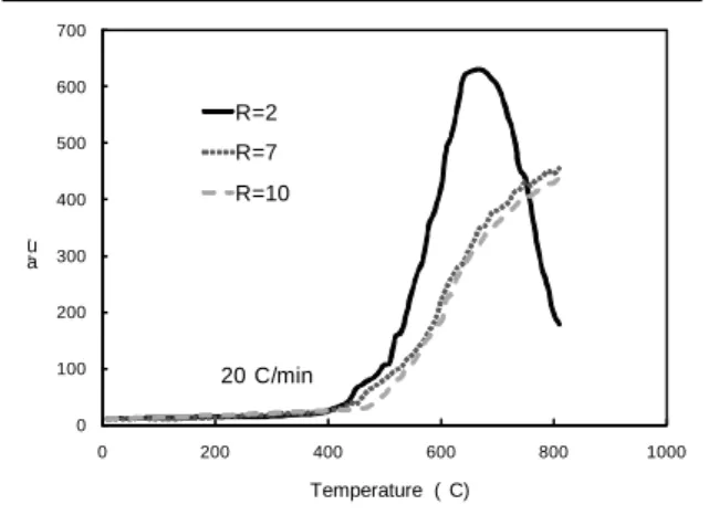
Figure 4 displays the evolution of the hydrogen flow released during TPD measurements for three distinct SiN stoichiometries: R = 2 (n = 2.98 – x = 0.35); R = 7.7 (n = 2.03 – x = 0.78); R = 10 (n = 1.98 – x = 0.81). All the films begin to release hydrogen at around 400°C. For the Si-richest SiN (R = 2), the hydrogen desorption is much faster than for the other samples. Indeed, the gas flow increases drastically from 440 to 680°C then decreases as rapidly from 680 to 810°C. At this temperature, the layer appears to have released the quasi-totality of its hydrogen. On the other hand, H-exodiffusion from “N-rich” SiN is much slower: at 810°C the gas flow still increases, which means that a non-negligible amount of hydrogen remains in the film. For the studied samples, the hydrogen released at temperature as low as 440°C is thus attributed to the breaking of Si-H bonds. These results show as well that Si-H bonds are broken at around 650°C and that N-H bonds still resist to temperatures as high as 800°C. For the two “N-rich” samples (R = 10 and 7.7), the H desorption kinetics are similar, although their N-H and Si-H bond densities are different (Figure 3). Nevertheless, their respective stoichiometries and Si-N bond densities are really close, which indicates similar film densities. Dekkers et al. [9] showed that the diffusion coefficient of hydrogen decreases for increasing SiN density. Hence, the TPD results confirm that hydrogen diffusion and effusion is made easier in a Si-rich SiN, while it is slowed for “N-rich” SiN. The SiN density appears to be a key-parameter of the H-diffusion kinetics.
4. Surface Passivation
a. Capacitance-Voltage measurements
The positive fixed charge density Qf in the different SiN layers was determined thanks to C-V measurements. These charges correspond to electrical defects which charge state cannot vary in function of the electrical polarization of the MIS structure. For the SiN, it is generally admitted that the fixed charges are situated in the first 20nm of the layer [3]. Indeed, the constraints induced in this region give rise to a high defect density that can be electrically charged.
An example of C-V curve is displayed in Figure 5 for SiN with n = 1.98 (R = 10). The high flat band voltages obtained (here VFB = -22.8V) indicate high positive fixed charge densities (here Qf = 7.1×1012 cm-2). The Si dangling bond is the dominant deep defect in SiN films. Its predominant configuration is ⋅Si≡N3 (the so-called K centre), which create a high density of states in the middle of the gap [12, 51, 52]. The K centres, in their stable form N3≡Si+ (K+ centres) contribute primarily to the positive charge Qf. The Nitrogen dangling bond =N¯ can only be observed for stoichiometric and over-stoichiometric SiN (x > 1.33) [51]. Their contribution to the total charge can be neglected in our case (x < 0.81). On the other hand, defects introduced by the thin interface SiOxNy layer (< 2 nm) could increase Qf. The additional positive fixed charge would be generated by the following configurations: O3≡Si·, O2N≡Si· or ON2≡Si· [3]. The important counter-clockwise hysteresis effect observed for all
9
the samples can be attributed to slow states situated near the interface (1 to 3 nm), with a capture cross-section decreasing as these defects are situated farther from the interface [24]. The K centres are amphoteric with three charge states (+, 0, -) and are neutral when one electron is attached [51]. Hence, a strong negative polarization can induce electron emission from K° and K- centres situated near the interface. As these charges are created with the polarization, we will not consider their contribution to the total Qf.
For all the studied samples (Figure 6), the fixed charge density are greater than 1012 cm-2, which is very high in comparison with values reported for silicon oxide (~1010 to 1011 cm-2) [2]. Qf increases as the N-content of the SiN layer increases. This is consistent with the fact that the Si dangling bonds come to be more and more in their K+ (N3≡Si+) configuration. The simultaneous increase of the hysteresis effect with the N-content indicates an increasing slow states density, which hence confirms an increase of the K centre density. Consequently, for the SiN stoichiometries studied in this work (0.35 < x < 0.81), we can suppose that the field-effect passivation will be more efficient for N-rich SiN layers. However, the values obtained for the interface state density Dit are high (Dit = 3×1011 cm-2.eV-1 for the example shown in Figure 5) in comparison with values reported for silicon oxide (~ 1010 cm-2.eV-1) [2]. Even if the field-effect passivation should be efficient for all the stoichiometries, the high interface state density could affect it by increasing the recombination probability.
After the RTA process, Qf decreases for all the samples (Figure 6). This can be attributed to a neutralization of dangling bonds situated in the SiN (K centres) close to the interface by the hydrogen diffused from the SiN layer itself. Nevertheless, the final Qf values are still very high (>1012 cm-2) and the field-effect passivation should still be efficient. Furthermore, the high temperature step induced a strong reduction of Dit from ~1011 to ~1010 cm-2.eV-1 for the samples with R = 7.7 (n = 2.03) and R = 10 (n = 1.98 – the other values were not exploitable). As it will be developed in the following, this can be attributed to hydrogen passivation of surface silicon dangling bonds. This mechanism will be studied carefully as it plays an important role in the surface passivation process.
b. Surface passivation : as-deposited SiN layers
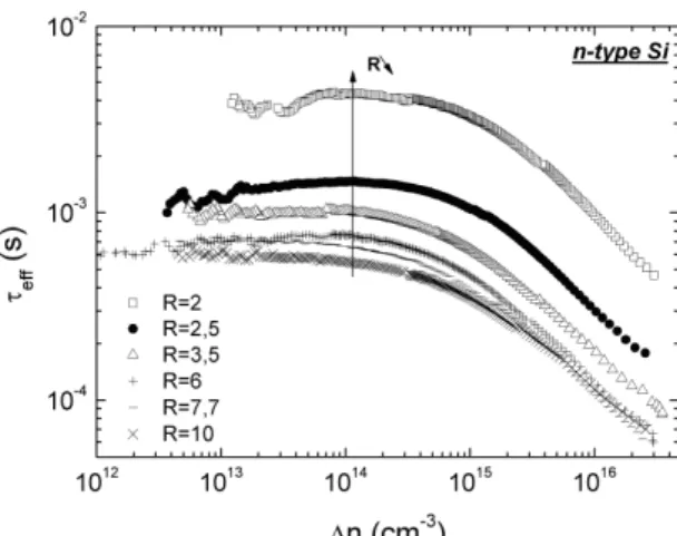
The evolution of effective minority carrier lifetime τeff in function of injection level ∆n is presented in Figure 7 for SiN layers deposited on n-type c-Si wafers. Table 1 shows the corresponding τeff values (∆n = 7×1014 cm-3) for the n-type and p-type samples. It also displays the extracted surface recombination velocities Seff assuming infinite bulk lifetime, which gives the upper limit of Seff (Eq. 3).
Firstly, for a same SiN stoichiometry, surface passivation is better achieved on n-type than on p-type silicon wafers. Following Eq. (1), the surface recombination rate is dependent of Qf (through ns and ps) and Dit, as we have already seen. Another important parameter which affects Seff is the substrate doping level (through ns, ps, n1 and p1). Here, the doping difference is too small to explain the better results obtained on n-type c-Si substrates: NA = 2.8×1015 cm-3 (p-type) and ND = 9.2×1014 cm-3 (n-type). Furthermore, surface recombination velocity depends strongly on the capture cross-sections σn and σp. The better surface passivation obtained for n-type c-Si (see Fig.2) could be explained by a large capture cross-section ratio of minority to majority charge carriers (σn/σp~100 at midgap). This would lead to more critical surface passivation for p-type silicon [31], although values for σn/σp may be discussed [52].
In all cases, the Seff values obtained are very low (see Table 1) and are a good result in comparison with values reported in the literature for low frequency PECVD reactors. Effective lifetime as high as 3.62 ms was found for the Si-richest SiN layer deposited on n-type c-Si, corresponding to Seff as low as 4 cm/s. With this kind of reactor, Schuurmans
10
obtained an optimal value of 45 cm/s for a FZ p-type c-Si with resistivity ρ = 1.9 Ω.cm [27]. Schmidt and Aberle reported values of 30 cm/s and 100 cm/s for FZ p-type samples with respective resistivities of 20 Ω.cm and 1.5 Ω.cm [52]. For n-type substrates (ρ = 10 Ω.cm),
they obtained Seff = 19cm/s. Even if our τeff results remain lower than the ones reported for direct high frequency and remote PECVD reactors [11, 53], the surface passivation quality of the SiN deposited with our LF-PECVD reactor is clearly satisfying, despite the fact that the Si substrate is subjected to ion bombardment during the SiN deposition.
Looking at different SiN stoichiometries, τeff increases when the Si-content of the SiN layer is increased for both the n- and p-type FZ c-Si samples (Table 1). This is consistent with results reported in the literature for different PECVD reactor configurations [53]. It should be noticed that Schmidt and Kerr [54] obtained an optimal effective lifetime for “stoichiometric” SiN (n = 1.9 – HF-PECVD), which they attributed to the use of diluted silane (5% in N2) as precursor gas. Hence, the surface passivation properties of as-deposited SiN seem to be strongly dependent on the deposition system and parameters.
Figure 8 shows the evolution of τeff according to the refractive index n of the different SiN layers, before and after the annealing. This graph displays as well the results obtained with mc-Si substrates: before annealing, the evolution of τeff according to the refractive index is comparable with the one observed with monocrystalline substrates. However, τeff is a global measure that integrates Seff and τb and it becomes more difficult to identify the relative contribution of each parameter in the case of mc-Si samples. Our PCD measurements were completed by Seff and τb cartographies obtained by the µW-PS method. Figures 9 and 10 show the results for the mc-Si substrates coated by Si-rich SiN (R = 2 – n = 2.98) and “N-rich” SiN (R = 6 – n = 2.08), before and after annealing. Seff and τb values are heterogeneous as expected for mc-Si samples: Seff varies for example between few cm.s-1 and more than 1000 cm.s-1 for as-deposited layers (Figure 9.a). Better results are clearly obtained when the Si-rich silicon nitride is used as passivation layer, with a mean value of Sm=215cm.s-1 and Seff remaining lower than 150 cm.s-1 on an important part of the sample surface. On the other hand, Seff is always higher than 150 cm.s-1 for the “N-rich” sample. These results are in agreement with the ones obtained with the FZ c-Si substrates. They confirm that, after LF-PECVD deposition, the different SiN layers provide good surface passivation and that Si-rich SiN leads to the lowest surface recombination velocities.
c. Surface passivation after a high temperature step
After a high temperature step (simulating the co-firing of solar cell contacts), τeff decreases strongly for c-Si samples coated with Si-rich SiN (Figure 8). If we assume that τb remains almost constant after the RTA process, Seff increases strongly from 4 cm.s-1 to 150 cm.s-1 for the n-type substrate coated with the Si-richest SiN (R = 2 – n = 2.98). On the other hand, the surface passivation quality provided by the “N-rich” alloys (R = 10, 6, 7.7) hardly changes and even increases. An identical behaviour was found for mc-Si samples (Figures 8 and 9.b). The cartographies show that the RTA process induced a strong deterioration of the surface passivation quality provided by the Si-rich SiN (R = 2), with Seff greater than 700 cm.s-1 for a large part of the analyzed surface. The entire surface seems affected and there is no clear correlation between the initial and the final Seff value. On the other hand, Seff is strongly reduced for the “N-rich” sample (R = 6): Seff is lower than 150 cm.s-1 on a large part of the substrate area, which results in a low average value (Sm = 350 cm.s-1). It is worth noting however that the regions of the mc-Si wafer which exhibit high surface recombination velocities (> 700 cm.s-1) appear difficult to improve. Nevertheless, for n- and p-type Si samples, the best surface passivation after annealing is obtained for SiN with low refractive index (n ~ 2 – 2.1).
11
d. Discussion
Our results show a high surface passivation quality for as-deposited samples, with Seff decreasing with the Si-content of SiN. At first, this seems in contradiction with the C-V results from which field-effect passivation was supposed to be less efficient in this case. However, it should be reminded that Qf is very high for all the stoichiometries (> 1012 cm-2) and that such fixed charge densities should provide a good field-effect passivation regardless the stoichiometry. On the other hand, Schmidt and Aberle [52] suggested that Qf must be drastically reduced to ~1011cm-2 under illumination (PCD measurements case) in comparison with the values determined by dark C-V measurements: illumination could lift the quasi-Fermi level Φn above the energy level of the K+ centres, leading to their neutralization. This could make the field-effect passivation less efficient under illumination. Whatever this issue is, the interface state density Dit appears to be a key-parameter when comparing different SiN stoichiometries. For Si-rich SiN, an important flow of the very reactive silane (SiH4) during the PECVD process could provide more H-radicals to the plasma. This would contribute to an efficient neutralization of interface states thanks to Si-H bonds, and thus reduce the corresponding Dit. Mäckel and Lüdemann [12] consider that the Si-H bond density in the SiN layer is a quality indicator of surface passivation. As it was demonstrated thanks to FTIR measurements, Si-rich SiN exhibits a higher Si-H bond density, which can be correlated to a better passivation of the dangling bonds at the silicon surface. Furthermore, we can suppose that such layers induce less constraint with the silicon substrate, and hence less surface defects. Hence, the high K+ centres density in “N-rich” SiN appears to be not sufficient enough to compensate the higher interface state density.
In contrast, after a high temperature step, the best surface passivation is provided by low refractive index SiN. The chemical and structural analysis of these SiN layers showed that they are denser and thermally more stable than Si-rich samples. The hydrogen desorption kinetics are also different according to the SiN stoichiometry, Si-rich SiN releasing faster a higher hydrogen concentration than “N-rich” SiN. According to Dekkers et al. [9], a low density material would induce the release of hydrogen in the molecular form (H2). On the contrary, a denser SiN would make the hydrogen desorption slower but its atomic form would be advantaged. We can thus suppose that the hydrogen is widely released in its molecular form out of the sample in the case of Si-rich SiN, with a more “opened” structure. Furthermore, a great part of the Si-H bonds at the SiN/Si interface would be broken by the high temperature step, leading to the increase of Dit and Seff. It is however possible that part of the hydrogen stocked at the interface during the deposition can diffuse in its atomic form towards the Si substrate and participate hence to bulk defects passivation. On the opposite, SiN with a higher N-content implies a denser material and the hydrogen contained in the film would diffuse in its atomic form towards the SiN/Si interface. This is supported by C-V results, which showed a decrease of Dit after annealing for samples with R = 7.7 (n = 2.03) and R = 10 (n = 1.98). As suggested by Sopori [4], atomic hydrogen diffusion would be assisted by defects and the high defect concentration at the SiN/Si interface would make easier the diffusion of this element towards the substrate. Moreover, we can assume that bulk defects reinforce this traps-driven hydrogen diffusion. This would explain why surface passivation changes are dependent of the region observed of the mc-Si substrate (R = 6) and why the relative Seff enhancement is more important for multicrystalline silicon substrates than for monocrystalline ones. Hence, all these results support that low refractive index SiN leads to the best Seff after the RTA process and that this can be attributed to an appropriate SiN structure and density.
12
5. Bulk Passivation
Figure 10 shows the bulk lifetime τb cartographies of the same mc-Si samples before and after the high temperature step. For the as-deposited samples (Figure 10.a), τb is relatively high for the whole surface analyzed: the measured values lay between 100 µs and 300 µs, which demonstrates the high quality of the mc-Si substrates used. However, the sample coated by the Si-rich SiN (R = 2) presents a higher mean value of bulk lifetime (τb = 190 µs). The two mc-Si substrates used were neighbouring wafers of a same ingot and we can assume that they present similar bulk structural properties. Hence, the observed differences could be attributed to hydrogen passivation of bulk defects during the PECVD process. Indeed, a higher SiH4 flow during the SiN deposition could provide higher H-radicals concentration in the plasma and these atoms could penetrate deep in the Si bulk substrate at the considered elaboration temperatures (370°C).
The RTA process induced a clear enhancement of τb for the mc-Si sample coated with “N-rich” SiN (R = 6 – Figure 10.b), the mean value going from 140 µs to 210 µs. This value remained constant for the Si-rich SiN sample. However, a detailed observation of the corresponding cartography shows that bulk lifetime increased for a non negligible part of the sample. Thus, these results confirm that hydrogenation occurs during annealing and increases the minority carrier lifetime in the bulk of the silicon substrate. Furthermore, if we consider that the hydrogen contained in Si-rich SiN (less dense) is widely released in its H2 form, it appears that such molecules will not participate to the defect passivation. In this case, the increase of τb could be due to neutralization of defects thanks to the atomic hydrogen initially stocked at the interface during SiN deposition. It could also be due to diffusion of hydrogen trapped in the bulk of the substrate itself, as some regions show a decrease of τb after annealing. On the other hand, a high increase of τb is observed on the whole surface of the sample coated with the low refractive index SiN. This confirms that important atomic hydrogen diffusion occurs from the SiN towards the mc-Si substrate during the high temperature step, neutralizing the defects situated deeply in the sample. The hydrogen chemical bonding as well as the mass density of the SiN layer appears to be key parameters for an efficient substrate hydrogenation.
6. Conclusion
As it was recently highlighted by other research groups, the SiN mass density (and hence the Si-N bond density) appears to be a good indicator for optimum surface and bulk passivation after annealing. Indeed we showed a direct correlation between hydrogen desorption mechanism and the SiN Si-content. As the latter was correlated to the mass density, a clear relation was found with the SiN ability to release hydrogen in its atomic form, and hence to provide good final surface and bulk passivation. On the other hand, for as-deposited SiN films, a better surface and volume passivation is obtained thanks to Si-rich SiN. Here, a higher gas flow of silane during SiN deposition would lead to a plasma composition richer in hydrogen. The more “opened” structure of such Si-rich layers would facilitate the diffusion of H-radicals towards the silicon substrate during the short PECVD process. Hence, this would result in defect neutralization at the surface and deep in the bulk of the silicon substrate.
This study reveals thus that low refractive index SiN layers (n ~ 2 – 2.1) provide the best surface and bulk passivation properties after the RTA process. This is interesting for photovoltaic applications as such layers can be used efficiently as antireflective coating of mc-Si solar cells. Furthermore, SiN is of great interest for other photovoltaic structures. Indeed, current work is under investigation at INL-INSA to develop an optimized
13
ARC/passivation layer for the front surface of Rear Contacted Cells (RCC). The fabrication of such solar cells does not involve a high temperature firing step. As surface passivation is a crucial issue in this case, a combination of low/high refractive index SiN layers could provide at the same time higher photon transmission through the optimization of the double antireflection coating, and higher surface passivation thanks to the Si-richer SiN layer in contact with the Si substrate. Moreover, investigation is under progress in order to apply SiN as passivation layer of the rear surface of conventional solar cells, which would be an alternative to the thick Al Back Surface Field (BSF) [55]. This issue has been a difficult one for a long time as the high positive charge density has been an important obstacle for proper solar cell operation (see e.g. [56]). However, recent works have showed that the combination of a local BSF and a SiN passivation layer applied to thin substrates can lead to good photovoltaic results [57]. Even if the physical reasons of such results stay unclear, this is encouraging for further investigation. In particular, as we have highlighted here that the SiN chemical structure is dependent on the deposition system and parameters, an interesting research task is the study of SiN deposited thanks to dilute silane. Indeed, as the deposition reactions and kinetics will be clearly different, the obtained material will present a distinct chemical structure in terms of mass density, hydrogen content and positive fixed charge density. Thus, it seems still possible to take advantage of the interesting optical and passivation properties of hydrogenated silicon nitride.
14
References
[1] F. Duerinckx and J. Szulfcik. Defect passivation of industrial multicrystalline solar cells based on PECVD silicon nitride. Solar Energy Materials & Solar Cells 2002, 72, pp. 231-246.
[2] C. Leguit et al. Low temperature surface passivation for silicon solar cells. Solar Energy Materials and Solar Cells 1996, 40, pp. 297-345.
[3] A.G. Aberle Overview on SiN Surface Passivation of crystalline silicon solar cells. Solar Energy Mat. & Sol. Cells 2001, 65, pp. 239-248.
[4] B.L. Sopori, Y. Zhang, R. Reedy. H Diffusion for Impurity and Defect Passivation: A Physical Model for Solar Cell Processing. Proc. of the 29th IEEE-Photovoltaic Specialists Conference, 2002, New Orleans (USA).
[5] T. Lauinger, A.G. Aberle and R. Hezel. Comparison of direct and remote PECVD silicon nitride films for low-temperature surface passivation of p-type crystalline silicon. Proc. of 14th European. Photovoltaic Solar Energy Conference, 1997, Barcelona (Spain), p. 853.
[6] B. Sopori et al. A comprehensive model of hydrogen transport into a solar cell during silicon nitride processing for fire-through metallization. Proc. of the 31st Photovoltaic Specialists Conference, Jan.
2005, Orlando (USA), pp. 1039 – 1042.
[7] V. Yelundur, A. Rohatgi, J.I. Hanoka, R. Reedy. Beneficial impact of low frequency pecvd SiNx :H-induced hydrogenation in high efficiency string ribbon silicon solar cells. Proc. of 19th European. Photovoltaic Solar Energy Conference 2004, Paris (France), pp. 951-954.
[8] J. Hong et al. Influence of the high-temperature ‘‘firing’’ step on high-rate plasma deposited silicon nitride films used as bulk passivating antireflection coatings on silicon solar cells. Journal of Vacuum Science and Technology B 2003, 21(5), pp. 2123-2132.
[9] H.F.W. Dekkers, L. Carnel, G. Beaucarne and W. Beyer. Diffusion mechanism of hydrogen through PECVD SiNx:H for a fast defect passivation of mc-Si solar cells. Proceedings of the 20th European Photovoltaic Solar Energy Conference, June 2005, Barcelona (Spain).
[10] W.D. Eades and R.M. Swanson. Calculation of surface generation and recombination velocities at the Si-SiO2 interface. Journal of Applied Physics 1985, 58, p. 4267.
[11] A. Cuevas, M.J. Kerr and J. Schmidt. Passivation of crystalline silicon using silicon nitride. 3rd World Conference on Photovoltaic Energy Conversion, May 2003, Osaka (Japan).
[12] H. Mäckel and R. Lüdemann. Detailed study of the composition of hydrogenated SiNx layers for high-quality silicon surface passivation. Journal of Applied Physics 2002, 92(5), pp. 2602-2609.
[13] B. Sopori. Dielectric films for Si solar cell applications. Journal of Electronic Materials, 2005, 34(5), pp. 564-570.
[14] J.Y. Lee, J. Divker, S. Rein and S.W. Glunz. Investigation of various surface passivation layers using oxide/nitride stacks of silicon solar cells. Proceedings of the 3rd World Conference on Photovoltaic Energy Conversion, 2003, Osaka (Japan).
[15] A.W. Weeber, H.C. Rieffe, I.G.Romijn, W.C. Sinke, W.J. Soppe. The fundamental properties of SiNx:H that determine its passivating qualities. Proc. of the 31st Photovoltaic Specialists Conference 2005, Orlando (USA), pp. 1043-1046.
[16] W.A. Lanford and M.J. Rand. The hydrogen content of plasma-deposited silicon nitride. Journal of Applied Physics 1978, 49(4), pp. 2473-2477.
[17] J. Hong et al. Structural film characteristics related to the passivation properties of high-rate (>0.5 nm/s) plasma deposited a-SiNx:H. Proc. of the 3rd World Conf. on Photovoltaic Energy Conversion 2003, Osaka (Japan) , p. 1158.
[18] I. Romijn et al. SiNx:H passivation: How to obtain the maximum efficiency for mc-Si solar cells. Workshop on the fundamentals of a-SiNx:H in industrial solar cell processing, 3rd Nov. 2005, IMEC,
Leuven (Belgium). All the presentations are available on-line :
<http://www.ipcrystalclear.info/Paginas/Overige%20webpaginas/Programme%20and%20presentations %20SiNx%20fundamentals%20workshop.aspx> (last consultation 23/05/08)
[19] I.G.Romijn, W.J. Soppe, H.C. Rieffe, A.R. Burgers, A.W. Weeber. Passivating mc-Si solar cells using SiNx:H: Magic or Physics. Proc. 20thEuropean Photovoltaic Solar Energy Conf. 2005, Barcelona (Spain) , pp. 1352-1355.
15
[20] A. Cuevas, F. Chen, J. Tan, H. Mäckel, S. Winderbaum and K. Roth. FTIR analysis of microwave excited PECVD silicon nitride. Proc. of the 4th World Conf. on Photovoltaic Energy Conversion 2006, Waikoloa (USA),pp. 1148-1151.
[21] F. Chen, I. Romijn, A. Weeber, J. Tan, B. Hallam, and J. Cotter. Relationship between PECVD silicon nitride film composition and surface and edge passivation. Proc. of the 22nd European Photovoltaic Solar Energy Conference 2007, Milan (Italy), pp. 1053-1060.
[22] G.E. JELLISON and F.A. MODINE. Parameterization of the optical functions of amorphous materials in the interband region. Applied Physics Letters 1996, 69(3), pp.371-373, 2137.
[23] G.K. REEVES and H.B. HARRISON. Obtaining the specific contact resistance from transmission line model measurements. Electron Device Letters 1982, 3(5), pp. 111-113.
[24] E.H. Nicollian and J.R. Brews. MOS Physics and Technology. New-York: Wiley-Interscience 1982. [25] R.A. Sinton and A. Cuevas. Contactless determination of current-voltage characteristics and
minority-carrier lifetimes in semiconductors from quasi-steady-state photoconductance data. Applied Physics Letters 1996, 69(17), pp. 2510-2512.
[26] A. Cuevas and D. Macdonald. Measuring and interpreting the lifetime of silicon wafers. Solar Energy
2004, 76(1-3), pp. 255-262.
[27] F. Schuurmans. Surface passivation of silicon by PECVD silicon nitride. PhD Thesis 1998, University of Utrecht (The Netherlands), 134 p.
[28] Palais O. And Arcari A. Contactless measurement of bulk lifetime and surface recombination velocity in silicon wafers. Journal of Applied Physics 2003, 93(8), pp. 4686-4690.
[29] A. Cuevas, M. Stocks, D. Mcdonald, M. Kerr and C. Samundsett. Recombination and trapping in multicrystalline silicon. IEEE Transactions on Electron Devices 1999, 46(10), pp. 2026-2034.
[30] H.R. Philipp. Silicon nitride (Si3N4) (Noncrystalline). In: Handbook of optical constants of solids 1985,
vol. 1, Ed. E.D. PALIK. New-York, USA: Academic Press, pp. 771-774.
[31] S. De Wolf, G. Agostinelli, G. Beaucarne and P. Vitanov. Influence of stoichiometry of direct plasma-enhanced chemical vapor deposited SiNx films and silicon substrate roughness on surface passivation. Journal of Applied Physics 2005, 97, p. 063303.
[32] J-F.Lelièvre et al. Comparative study of structural and optical properties of silicon nitride SiNx:H deposited by PECVD. Proc. of the 20th European Photovoltaic Solar Energy Conference 2005, Barcelona (Spain), pp. 1142-1145
[33] A. Dollet, J. P. Couderc and B. Despax. Analysis and numerical modelling of silicon nitride deposition in a plasma-enhanced chemical vapor deposition reactor. Part I: bidimensional modelling. Plasma Sources Science and Technology 1995, 4, pp. 94-106.
[34] H. Caquineau, G. Dupont, B. Despax and J.P. Couderc. Reactor modelling for radio frequency plasma deposition of SiNxHy: Comparison between two reactor designs. Journal of Vacuum Science & Technology A 1996, 14(4), pp. 2071-2082.
[35] J-F. Lelièvre, H. Rodriguez, E. Fourmond, S. Quoizola, M. Lipinski, D. Araujo, G. Bremond, M. Lemiti. Electro-optical characterisation for the control of silicon nanocrystals embedded in SiNx:H films. Physica Status Solidi (c) 2007, 4(4), pp. 1554-1559.
[36] J-F. Lelièvre et al. Evidence of intrinsic silicon nanostructures formation in SiN matrix deposited by various low temperature CVD techniques. Physica Status Solidi (c) 2007, 4(4), pp. 1401-1405.
[37] M.A. Green et al. Progress with all-silicon tandem cells based on silicon quantum dots in a dielectric matrix. Proc. of 21st European. Photovoltaic Solar Energy Conference. 2006, Dresden (Germany), pp. 10-14.
[38] V.A. Gritsenko, K.S. Zhuravlev, A.D. Milov, H. Wong, R.W.M. Kwok, J.B. Xu. Silicon dots/clusters in silicon nitride: photoluminescence and electron spin resonance. Thin Solid Films 1999, 353, pp. 20-24. [39] H.R. Philipp. Optical Properties of Silicon Nitride. Journal of the Electrochemical Society 1973, 120, p.
295.
[40] G.M. Ingo, N. Zacchetti, D.Della Sala and C. Coluzza. X-ray photoelectrons spectroscopy investigation on the chemical structure of amorphous silicon nitride (a-SiNx). Journal of Vacuum Science and Technology 1989, 7(5), pp.3048-3055.
[41] E. Bustarret et al. Configurational statistics in a-SixNyHz alloys: A quantitative bonding analysis. Physical Review B 1998, 38(12), pp. 8171-8183.
[42] Stefan Dauwe. Low temperature surface passivation of crystalline silicon and its application to the rear side of solar cells. PhD Thesis 2004, Hannover Universität (Germany), page 76.
16
[43] J-F. Lelièvre, A. Kaminski, J-P. Boyeaux, R. Monna, M. Lemiti. Optical properties of PECVD and UVCVD SiNx:H antireflection coatings for silicon solar cells. Proc. of the 31st IEEE Photovoltaic Specialists Conference 2005, Orlando (USA), pp. 1111-1114.
[44] J-F.Lelièvre et al. Correlation of optical and photoluminescence properties in amorphous SiNx:H thin films deposited by PECVD or UVCVD. Thin Solid Films 2006, 511-512, p. 103.
[45] G. Morello. Hydrogen content of amorphous PECVD SiNx :H films by infrared spectroscopy and hydrogen forward scattering results. Journal of Non-Crystalline Solids 1995, 187, pp. 308-312.
[46] V. Verlaan et al. Hydrogen evolution in hot-wire deposited SiN with calibrated FTIR proportionality constants. Workshop on the fundamentals of a-SiNx:H in industrial solar cell processing, 3rd Nov. 2005,
IMEC, Leuven, Belgium. Presentation available on-line (see Ref. 18)
[47] I.V. Afanasyev-Charkin et al. Amorphous silicon nitride films of different composition deposited at room temperature by pulsed glow discharge plasma immersion ion implantation and deposition. Journal of Vacuum Science and Technology 2004, 22(6), pp. 2342-2346.
[48] Z. Yin and F.W. Smith. Optical dielectric function and infrared absorption of hydrogenated amorphous silicon nitride films: Experimental results and effective-medium-approximation analysis. Physical Review B 1990, 42(6), pp. 3666-3675.
[49] F. Giorgis et al. Optical, structural and electrical properties of device-quality hydrogenated amorphous silicon nitrogen films deposited by plasma-enhanced chemical vapour deposition. Philosophical Magazine B 1998, 77(4), pp. 925-944.
[50] F. Jiang, M. Stavola, A. Rohatgi, D. Kim, J. Holt, H. Atwater, J. Kalejs. Hydrogenation of Si from SiNx(H) films: Characterization of H introduced into the Si. Applied Physics Letters 2003, 83(5), pp.931-933.
[51] J. Robertson, W.L. Warren and J. Kanicki. Nature of Si and N dangling bonds in silicon nitride. Journal of Non-Crystalline Solids 1995, 187, pp. 297-300.
[52] J. Schmidt and A.G. Aberle. Carrier recombination at silicon-silicon nitride interfaces fabricated by plasma enhanced chemical vapor deposition. Journal of Applied Physics 1998, 85(7), pp. 3626-3633. [53] J. Schmidt and S. Dauwe. Surface Passivation of Silicon Solar Cells using SiNx : The Effect of Space
Charge Recombination. Workshop on the fundamentals of a-SiNx:H in industrial solar cell processing,
3rd Nov. 2005, IMEC, Leuven, Belgium. Presentation available on-line (see Ref. 18)
[54] J. Schmidt and M. Kerr. Highest-quality surface passivation of low-resistivity p-type silicon using stoichiometric PECVD silicon nitride. Solar Energy & Solar Cells 2001, 65, pp. 585-591.
[55] J. Dupuis, E. Fourmond, O. Nichiporuk, F. Gibaja, M. Lemiti. Rear passivation schemes and their applications in industrial silicon solar cells, to be presented in the 23rd European Photovoltaic Solar Energy Conference, 2008, Valencia (Spain).
[56] S. Dauwe, L. Mittelstädt, A. Metz and R. Hezel. Loss mechanisms in silicon nitride rear surface passivation for silicon solar cells. Proc. of the 17th European Photovoltaic Solar Energy Conference,
2001, Munich (Germany).
[57] L. Janßen, M. Rinio, D. Borchert, H. Windgassen, D.L. Batzner and H. Kurz. Thin bifacial multicrystalline silicon solar cells for industrial production. Proc. of 21st European. Photovoltaic Solar Energy Conference, 2006, Dresden (Germany).
17
Tables
Table 1: Effective lifetime τeff and surface recombination velocity Seff of n- and p-type FZ c-Si samples coated with different as-deposited c-SiN (∆n = 7.1014 cm-3).
τeff (µs) Seff (cm.s-1) R=NH3/SiH4 x=N/Si n(605 nm) n p n p 2 0.35 2.98 3620 1090 4 14 2.5 0.42 2.69 1170 437 13 34 3.5 0.49 2.47 722 233 21 65 6 0.71 2.08 531 231 28 65 7.7 0.78 2.03 456 221 33 68 10 0.81 1.98 400 202 38 75
18
Figures
0,2 0,3 0,4 0,5 0,6 0,7 0,8 0,9 1,0 1,8 2,0 2,2 2,4 2,6 2,8 3,0 3,2 x mesured x calculated - Eq. (4) n ( 6 0 5 n m ) x = N/Si PECVD (440kHz)Figure 1: Evolution of the refractive index n(605 nm) according to the SiN stoichiometry
x = N/Si (measured values by XPS and estimated values thanks to Eq. 4) .
Figure 2: Comparison of the hydrogen profile obtained by SIMS for two distinct SiN
compositions (R = 2 / n = 2.98 and R = 7.7 / n = 2.03). The respective silicon signals (Si28) were adjusted at the same level in the Si substrate.
3600 3400 3200 3000 R=7,7 R=10 R=15 A b s o rb a n c e ( a .u .) Wavenumber (cm-1) R=30
Figure 3: Evolution of the N-H stretching absorption band measured by FTIR for different
19 0 100 200 300 400 500 600 700 0 200 400 600 800 1000 R=2 R=7 R=10 a .u . Temperature ( C) 20 C/min
Figure 4: Hydrogen desorption profile according to the temperature obtained by TPD for
three different SiN coatings (R = NH3/SiH4).
-28 -26 -24 -22 -20 -18 0 1 2 3 4 5 6 7 8 9 10 C a p a c it a n c e ( p F ) Bias Voltage (V) 1 kHz 10 kHz 100 kHz
Figure 5: Typical Capacitance-Voltage curve obtained at different frequencies for the sample
with R = 10 (n = 1.98). 2,0 2,2 2,4 2,6 2,8 3,0 1 2 3 4 5 6 7 8 as-deposited RTA fired Qf (x 1 0 1 2 c m -2 ) ni(605nm)
Figure 6: Fixed charge density Qf before and after annealing according to the initial refractive index ni(605 nm). The curves are to guide the eye.
20
Figure 7: Effective lifetime τeff according to the injection level ∆n for n-type samples coated with SiN of different stoichiometries (indicated by the gas flow ratio R = NH3/SiH4).
2,0 2,2 2,4 2,6 2,8 3,0 101
102
103
p type mc-Si p type mc-Si - RTA
τ eff ( µ s ) n type c-Si n type c-Si - RTA p type c-Si p type c-Si - RTA
ni(605nm)
Figure 8: Effective lifetime τeff (∆n = 7.1014 cm-3) before and after annealing according to the SiN initial refractive index ni(605 nm).
21 (a) R = 2 / n = 2.98 / Sm = 215 cm.s -1 R = 6 / n = 2.08 / Sm = 500 cm.s -1 A s -d e p o s it e d (b) R = 2 / Sm = 610 cm.s -1 R = 6 / Sm = 350 cm.s -1 R T A a n n e a le d
Figure 9: Surface recombination velocity Seff cartographies of p-type mc-Si samples (a) after SiN deposition and (b) after RTA firing (Sm correspond to average values).
(a) R = 2 / n = 2.98 / ττττb = 190 µs R = 6 / n = 2.08 / ττττb = 140 µs A s -d e p o s it e d (b) R = 2 / ττττb = 190 µs R = 6 / ττττb = 210 µs R T A a n n e a le d
Figure 10: Bulk lifetime τb cartographies of p-type mc-Si samples (a) after SiN deposition and (b) after RTA firing (The indicated τb values correspond to average values). The lines
22
situated in the lower left angle are measurement artefacts and should not be taken into account.