HAL Id: hal-01162158
https://hal.archives-ouvertes.fr/hal-01162158
Submitted on 15 Jun 2015
HAL is a multi-disciplinary open access
archive for the deposit and dissemination of
sci-entific research documents, whether they are
pub-lished or not. The documents may come from
L’archive ouverte pluridisciplinaire HAL, est
destinée au dépôt et à la diffusion de documents
scientifiques de niveau recherche, publiés ou non,
émanant des établissements d’enseignement et de
Very low-temperature epitaxial growth of Mn5Ge3 and
Mn5Ge3C0.2 films on Ge(111) using molecular beam
epitaxy
Matthieu Petit, Lisa Michez, Charles-Emmanuel Dutoit, Sylvain Bertaina,
Voicu Dolocan, Vasile Heresanu, Mathieu Stoffel, Vinh Le Thanh
To cite this version:
Matthieu Petit, Lisa Michez, Charles-Emmanuel Dutoit, Sylvain Bertaina, Voicu Dolocan, et al.. Very
low-temperature epitaxial growth of Mn5Ge3 and Mn5Ge3C0.2 films on Ge(111) using molecular beam
epitaxy. Thin Solid Films, Elsevier, 2015, 589, pp.427-432. �10.1016/j.tsf.2015.05.068�. �hal-01162158�
Very low-temperature epitaxial growth of Mn
5Ge
3and
Mn
5Ge
3C
0.2films on Ge(111) using molecular beam
epitaxy
Matthieu Petit∗
Aix-Marseille Universit´e, CNRS, CINaM UMR 7325, 13288, Marseille, France. Lisa Michez∗
Aix-Marseille Universit´e, CNRS, CINaM UMR 7325, 13288, Marseille, France. Charles-Emmanuel Dutoit∗
Aix-Marseille Universit´e, CNRS, IM2NP UMR7334, 13397 cedex 20, Marseille, France. Sylvain Bertaina∗
Aix-Marseille Universit´e, CNRS, IM2NP UMR7334, 13397 cedex 20, Marseille, France. Voicu O. Dolocan∗
Aix-Marseille Universit´e, CNRS, IM2NP UMR7334, 13397 cedex 20, Marseille, France. Vasile Heresanu∗
Aix-Marseille Universit´e, CNRS, CINaM UMR 7325, 13288, Marseille, France. Mathieu Stoffel∗
Universit´e de Lorraine, UMR CNRS 7198, Institut Jean Lamour, BP 70239, 54506 Vanduvre-ls-Nancy, France
Vinh Le Thanh∗
Aix-Marseille Universit´e, CNRS, CINaM UMR 7325, 13288, Marseille, France.
Abstract
C-doped Mn5Ge3compound is ferromagnetic at temperature up to 430 K. Hence
it is a potential spin injector into group-IV semiconductors. Segregation and diffusion of Mn at the Mn5Ge3/Ge interface could severely hinder the efficiency
∗Corresponding author
Email address: [email protected] (Matthieu Petit)
of the spin injection. To avoid these two phenomena we investigate the growth of Mn5Ge3and C-doped Mn5Ge3films on Ge(111) substrates by molecular beam
epitaxy at room-temperature. The reactive deposition epitaxy method is used to deposit these films. Reflection high energy electron diffraction, X-ray diffrac-tion analysis, transmission electron microscopy and atomic force microscopy indicate that the crystalline quality is very high. Magnetic characterizations by superconducting quantum interference device and ferromagnetic resonance reinforce the structural analysis results on the thin films quality.
Keywords: Epitaxial growth, Low temperature, Reactive deposition epitaxy (RDE), Molecular Beam Epitaxy (MBE), Mn5Ge3, Ferromagnetic resonance
(FMR)
PACS: 81.15.Hi, 81.05.Bx, 8.35.Ct, 61.05.cp, 68.37.Lp, 76.50.+g, 75.50.Cc
1. Introduction
During the last decade a great deal of effort has been devoted to the con-trol of electron spins in semiconductor devices. Indeed semiconductor spin-tronics is believed to be a promising solution to develop beyond scaled metal-oxide-semiconductor devices. These components would offer several advantages
5
as nonvolatility, lower electric power consumption, increased data processing speed and integration densities [1]. The realization of practical spintronic de-vices requires an efficient electrical injection of spin-polarized electrons from a ferromagnet into the conduction band of a semiconductor, a subsequent spin-polarized detection as well as an effective manipulation of spin in the
semicon-10
ducting channel. Furthermore, the devices should be highly compatible with the already-existing silicon-based technology for easy technological implementation. A perfect control of the growth process of the materials layers and the interfaces between these layers will be required to manufacture efficient spintronic devices. Among other suitable materials Mn5Ge3 presents all the prerequisite
crite-15
ria necessary in spin devices: it is a well known ferromagnet with a magnetic ordering persisting up to the room temperature (TC = 297 K) [2], with an
ex-perimental spin polarization of P = 15±5% [3], and it has been demonstrated that Mn5Ge3thin films could be grown epitaxially on a Ge(111) with the
follow-ing orientation: Mn5Ge3(001)//Ge(111) with [100] Mn5Ge3//[1-10]Ge, without
20
the formation of any other phase [4, 5]. Moreover the value of the Curie tem-perature can be tuned in the range of 297-430 K by doping the Mn5Ge3 layers
by a carbon concentration Cxbetween x = 0 and 0.7. Such an enhancement has
been explained due to MnIIMnII interactions mediated by carbon incorporated
into interstitial sites of the Mn5Ge3 lattice [6]. The crystalline structure and
25
the epitaxial relationship between the Mn5Ge3Cx film and Ge(111) surface are
not modified by the carbon doping. Usually the Mn5Ge3 and Mn5Ge3Cxfilms
are grown by the so-called solid phase epitaxy (SPE) method which requires the co-deposition of Mn and C layers followed by annealing between 600 K and 920 K to activate the diffusion process.
30
Using the Mn5Ge3Cx/Ge heterostructure in the spintronic devices will
re-quire the investigation of the spin-polarized injection into germanium from the Mn5Ge3Cx. Even though very recently spin transport has been demonstrated in
Mn5Ge3/Ge/Mn5Ge3 nanowires [7, 8], spin transport in Mn5Ge3/Ge/Mn5Ge3
thin films has to be studied. Because of the poor quality of germanium
ox-35
ides, very few studies report their use as an efficient tunneling barrier [9]. This drawback leads to the spin injection into Ge directly from Mn5Ge3Cx thanks
to the tunneling effect through a narrow width Schottky barrier. The electrical properties of the Mn5Ge3Cx/Ge(111) Schottky contacts have been investigated
in previous works giving a Schottky barrier (SB) height between 0.30 and 0.56
40
eV [10, 11]. The value of the SB width can be tuned in order to reduce Fermi level pinning at the interface by creating an ultrashallow and ultranarrow high doped layer at the vicinity of the Mn5Ge3Cx/Ge(111) interface [12, 13]. Thus
the growth process of the Mn5Ge3Cxon the Ge(111) should preserve the
ultra-shallow layer. This might not be the case with the SPE method since it needs an
45
annealing to form the Mn5Ge3Cxcompound which can damage the high doped
layer because of dopants and/or Mn diffusion [14].
In this article we propose a room temperature (RT) reactive deposition
taxy (RDE) method for the C-doped Mn5Ge3 deposition that allows to grow
high crystalline quality films with abrupt interface on Ge(111). Low
temper-50
atures are indeed often used to reduce the segregation, diffusion, intermixing and island formation during growth processes of various materials like IV and III-V semiconductors or oxides [15, 16, 17, 18, 19, 20]. We have first focused on the early stage of the C-doped Mn5Ge3 thin films deposition by
follow-ing in-situ the intensity of the patterns of the reflection high-energy electron
55
diffraction (RHEED). We have then combined X-ray diffraction (XRD) and transmission electron microscopy (TEM) to assess the crystalline quality of the thin films. The crystallinity was eventually corroborated by magnetic charac-terizations such as superconducting quantum interference device (SQUID) and ferromagnetic resonance (FMR).
60
2. Experimental details
2.1. Growth process and in-situ RHEED monitoring
Mn5Ge3 and Mn5Ge3C0.2 thin films were grown by MBE (molecular beam
epitaxy) on Ge(111) substrates by means of conventional Ge and Mn Knudsen ef-fusion cells and a carbon sublimation source (SUKO) from MBE-Komponenten.
65
The base pressure of the MBE chamber was 2.7×10⁻⁸ Pa. Prior to deposition
of the thin films, the Ge substrates were chemically cleaned before introduction into the MBE chamber. Then the second part of the cleaning process consisted of an in-situ thermal outgassing at 720 K for several hours followed by flashed annealing up to 1020 K to remove the Ge surface oxide. After this process the
70
Ge(111) surface was checked by RHEED with a beam acceleration voltage of 30kV and exhibits a quite well defined c(2×4) reconstruction. A 15 nm thick Ge buffer layer was then deposited at a substrate temperature of 770 K followed by an annealing at 970 K during 10 minutes to insure a good starting surface prior to the growth of the Mn5Ge3 layers. These last steps were also monitored by in
75
real time RHEED to control the quality of the Ge(111) surface. Mn5Ge3 and
temperature on the Ge buffer layer. Cell fluxes were carefully calibrated using RHEED oscillations and a quartz microbalance to achieve the right stoichiome-try of the layers. The growth was monitored in situ by RHEED, the formation
80
of the Mn5Ge3 and Mn5Ge3C0.2 layers being confirmed by the observation of
the (√3 ×√3)R30◦ reconstruction characteristic of a Mn5Ge3film [5, 21].
2.2. Structural and topological characterizations
X-ray diffraction data were collected using a Panalytical XPert PRO diffrac-tometer with non-monochromatic CuKα1 radiation (λ = 1.541 ˚A). Data were
85
collected over a 2Θ range of 22-92◦ with a step size of 0.004◦. Transmission electron microscopy (TEM) investigations were performed at an accelerating voltage of 300 kV on a JEOL JEM-3010 instrument with a spatial resolution of 1.7 ˚A. Cross-sections samples were prepared with a precision ion polishing system (PIPS). The topographies of the samples were imaged by atomic force
90
microscopy (AFM) with a Nanoscope IIIA Multimode from Digital instruments on a 6×6 µm2 area.
2.3. Magnetic properties
The magnetic characterization of Mn5Ge3 and Mn5Ge3C0.2 have been
per-formed using a SQUID magnetometer Quantum Design MPMSXL working up
95
to 5T. Ferromagnetic resonance measurements were carried out on a conven-tional Bruker EMX spectrometer working at X band (9.39GHz). Samples of 2×2 mm2 were glued on quartz suprazil rode and cooled from room tempera-ture down to 80K. The static magnetic field was aligned perpendicular to the field. A modulation of the static field of 5 Oe at a frequency of 100 kHz is used
100
with a lock in amplifier to increase sensitivity and record the derivative of the FMR signal.
3. Results and discussion
3.1. Structural analysis
We have deposited Mn5Ge3 and Mn5Ge3C0.2 thin films of total thicknesses
105
of 300 nm. The growth rate of these films was 1.4 nm/min. It is well estab-lished that epitaxial Mn5Ge3films on Ge(111) exhibit a (
√
3 ×√3)R30◦surface reconstruction with Mn termination [21]. The RHEED observation of such a reconstruction consists in 1×1 streaks along [-110] azimuth and additional 1/3 and 2/3 ordered streaks between the 1×1 streaks along the [11-2] azimuth. The
110
RHEED technique thanks to its grazing incidence, allows to instantaneously re-veal not only the change in the surface morphology but also the surface structure during film growth and it is the proper tool to probe the very first deposited atomic layers of an epitaxial growth [22]. We followed the evolution of the RHEED pattern versus deposition time of Mn, Ge and C atoms on the Ge(111)
115
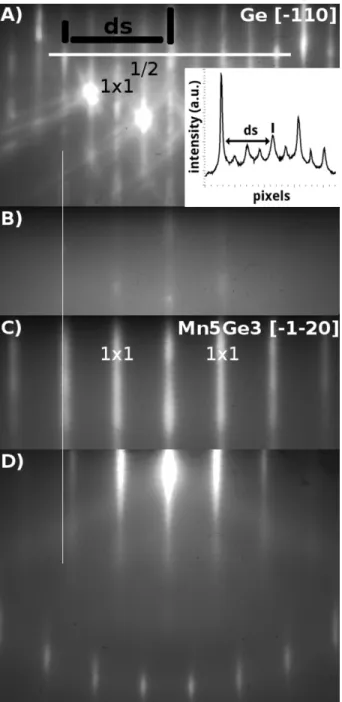
starting surface. This evolution is displayed on fig.1 for the Mn5Ge3C0.2 film.
Fig.1 A) shows the RHEED picture of the Ge[-110] azimuth of the Ge(111) starting surface. Sharp streaks and Kikuchi lines indicate a flat and ordered Ge surface. Fig.1 B) corresponds to the RHEED just after the beginning of the deposit: the Ge(111) surface features are disappearing and the background
120
intensity slightly increases. On fig.1 C) streaks of the Mn5Ge3 (
√
3 ×√3)R30◦ surface are appearing and sharpening as the film thickness increases indicating a 2D growth mode and a flat growth front. Fig.1 D) corresponds to the RHEED pattern at the end of the 300 nm thick deposit. The first Laue region is visi-ble at the bottom of the picture proving a high surface quality. Tapping mode
125
AFM images (not shown here) taken ex-situ after the complete deposition of the 300 nm thick films show flat surfaces with small RMS roughnesses of 1.28 nm and 2.17 nm for the Mn5Ge3C0.2and Mn5Ge3thin films respectively. From
these RHEED and AFM observation, the deposition at RT of the Mn5Ge3and
Mn5Ge3C0.2 thin films occurs in 2D growth mode. We have followed the
inten-130
sity of the RHEED pattern versus deposition time along the white line shown on fig.1 A). The inset on this figure give an example of this intensity profile along
Figure 1: Characteristic RHEED patterns recorded during the growth of the Mn5Ge3C0.2
thin film. A) pattern of the Ge(111) surface (inset: intensity profile of the RHEED image along the white horizontal line), B) pattern below 2 nm thick, C) pattern at a thickness of 4 nm and D) pattern at the end of the growth corresponding to a thickness of 300 nm. The white vertical line is a guide for the eyes positioned along the second 1×1 streak on the Ge[-110] azimuth of the Ge(111) surface.
Figure 2: Evolution of the streak shift ds defined on fig.1 A) versus the thickness of the deposition. Letters A), B), C) refer to the RHEED patterns of fig.1.
this line in the case of the cleaned Ge(111) surface in the Ge[-110] azimuth. The length ds defined also on fig.1 A) is measured between the specular and second 1×1 streaks. It was converted from pixels to angstroms using the streaks of
135
Ge[-110] azimuth as length reference. The variation of ds for the first 4 nm of the deposit is reported on fig.2.
The letters above the x-axis correspond to the different diffraction images in fig.1. The lattice length ds evolves rather quickly from its value on a Ge(111) surface to the value of thick Mn5Ge3C0.2 (0001) oriented films. The error bars
140
express the sharpness of the diffraction streaks used to calculate ds. We observe that the streaks remain blurry till 3 nm as the increase of the range of error bars proves it. It means that the C-doped Mn5Ge3film is formed and relaxes on
the Ge(111) surface over a transition layer of less than 3 nm thick. This value could be compared to the thickness of the ferromagnetic dead layer evaluated in
145
our previous work (fig.2 in ref [23]) which was extrapolated to 1.7±0.3 nm but further analysis are required to determine the nature of this interfacial layer as well as its magnetic properties. The last value of ds - 4.19 ˚A at a thickness of 4.2 nm - is very closed to the bulk lattice parameter of undoped Mn5Ge3which
is 4.15 ˚A. The slight difference may arise from two likely explanations: on one
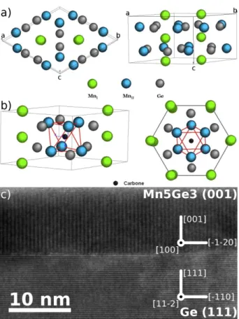
Figure 3: Colour online. a) Mn5Ge3lattice with the two Mn sub-lattices in two different
col-ors. b) carbon atom in the interstitial site of the Mn5Ge3lattice formed by MnIIoctahedron.
c) TEM cross sectional image of a Mn5Ge3thin film showing an atomic flat interface.
hand we measured the lattice shift from the digitalized profile of the RHEED intensity with an accuracy of hundredth angstrom even though the resolution of the aforesaid profile is limited by the size of pixels, on the other hand our value of ds regards a Mn5Ge3C0.2 films: carbon atoms are introduced in the
intersti-tial site of the Mn5Ge3 lattice which can induce an expansion of the in-plane
155
lattice parameter (fig.3 a) and b)) [6].
The TEM picture displayed in fig.3 c) is a typical cross section of the Mn5Ge3
and Mn5Ge3C0.2thin films grown on Ge(111) substrates. The interface is
atom-ically sharp and the well resolved lattice planes extending throughout the whole
160
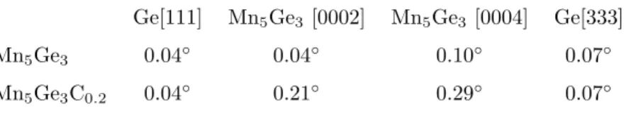
Ge[111] Mn5Ge3 [0002] Mn5Ge3 [0004] Ge[333]
Mn5Ge3 0.04◦ 0.04◦ 0.10◦ 0.07◦
Mn5Ge3C0.2 0.04◦ 0.21◦ 0.29◦ 0.07◦
Table 1: FWMH in degrees of the XRD 2Θ scans peaks of the Ge(111) substrate and Mn5Ge3
and Mn5Ge3C0.2 thin films
image reveal a high crystalline quality of the overgrown layer. We should men-tion that we did not observe threading dislocamen-tions even on TEM images of a larger scale although the lattice mismatch between the Mn5Ge3and Mn5Ge3C0.2
layers and the Ge(111) substrates is 3.7%. This was also the case for the SPE growth process [5].
165
The XRD 2Θ scan displayed in fig.4 a) was recorded on a Mn5Ge3film with
a thickness of 300 nm. The scan presents the Ge[111], [222] and [333] peaks related to the Ge(111) substrate and only the (0002) and (0004) reflections of the Mn5Ge3 film corresponding to the bulk parameters. These peaks are
170
doublets because of the CuKα1 and CuKα2 wavelengths, our XRD apparatus
being not equipped with a monochromator. The other smaller peaks come from the CuKβ and the CuKα1/2 radiations. We did not observe any other phase
even if Mn5Ge3 is not the most thermodynamically stable one according to
the Mn-Ge phase diagram [24] and different phases such as Mn11Ge8, Mn3Ge,
175
Mn5Ge2 have been obtained in the case of growth of MnxGey thin films on
various substrates [25, 26]. Such a phenomenon was already noticed for the SPE method and was attributed to the epitaxial stabilization of the Mn5Ge3
phase on the Ge(111) substrate, both being of a threefold symmetry [5]. Fig.4 b) shows a zoom on the regions of the (0002) and (0004) reflections with a set of
180
two peaks recording on the Mn5Ge3film already presented in fig.4 a) and on a
Mn5Ge3C0.2 film. Both films have a thickness of 300 nm. The full width at half
maximum (FWHM) of the different peaks resulting from the CuKα1wavelength
are summed-up in table 1.
From these values we observed that the crystallinity of the films is good which
Figure 4: a) XRD 2Θ scan of a 300 nm thick film of Mn5Ge3. b) Zoom of XRD 2Θ scans of
Mn5Ge3 and Mn5Ge3C0.2 thin films around the Mn5Ge3 [0002] and [0004] peak positions.
confirms the RHEED and TEM results. However it seems that the addition of carbon affects the crystalline quality. Looking at the peaks position in fig.4 b) and using Bragg’s law, we calculated the lattice parameters along the c axis of both films. The estimated disparity is 0.046 ˚A which means that there is a compression shift of about 1% between the Mn5Ge3 and Mn5Ge3C0.2 films.
190
This shift can be assigned to the variation of the lattice volume induced by the carbon atoms in the interstitial sites of the Mn5Ge3 lattice. The RHEED
data (fig.2) have shown an in-plane expansion of the lattice which seems to be counterbalanced by this lattice shrinking along the Mn5Ge3 (0001) axis. In
ref. [6], Slipukhina et al. calculated the increase of the MnII-MnII atomic
195
distance after introduction of carbon atoms in these interstitial sites and found a variation of 2.8%. This theoritical value on the MnII-MnII atomic distance is
rather consistent with our results regarding the whole lattice alteration. To be complete Gajdzik et al. observed a lattice compression in each direction (0.7% and 1.1% along the a and c axis respectively) caused by the incorporation of C
200
in Mn5Ge3Cx thin films prepared by sputtering at 680 K [27]. The difference
between these results and our observations is assumed to come from the growth processes.
3.2. Magnetic characterizations
Magnetization measurements have been performed on Mn5Ge3and Mn5Ge3C0.2
205
films of 15 nm thickness. The saturation magnetization (Ms) has been estimated
to be 1000 emu/cm3. These values are highly dependent on the knowledge of
the thickness of the films. However we did not notice a significant variation of Mswith carbon concentration, which remains at 1000±100 emu/cm3 in the
range of values generally observed in bulk [28] or layer [23] Mn5Ge3Cx.
210
The temperature dependence of the saturation magnetization measured in an applied field of H=1.0 T for different carbon concentrations is presented in figure 5. In order to compare the influence of the RT-RDE method on the magnetic properties of the Mn5Ge3Cx, we added Ms(T ) curves measured on Mn5Ge3Cx
samples grown by the SPE method [29] with various carbon concentrations:
x=0, 0.25 and 0.6. In the case of this method, the carbon concentration C=0.6 gives the highest Curie temperature at 430 K. Without carbon, no significant discrepancy is found. For low carbon concentrations, the shapes of the Ms(T )
curves slightly differ since the curve of the SPE x=0.25 sample has a rather broad tail towards the high temperatures. The Curie temperature is higher in
220
the case of the RDE x=0.2 sample (Tc=399 K) than in the case of the SPE
x=0.25 sample (Tc=345 K). These observations are explained by the fact that
the homogeneity of the distribution of carbon atoms is greatly enhanced by the RDE growth process compare to the SPE one leading to an improvement of the magnetic properties. To confirm this fact, the magnetizations of the Mn5Ge3
225
and Mn5Ge3C0.2 RDE samples are plotted versus the temperature normalized
by the Tc of each sample (Tc(Mn5Ge3)=296 K, Tc(Mn5Ge3C0.2)=399 K) in
the inset of fig.5. The curves are perfectly superimposed asserting the good homogeneity of the carbon distribution in the Mn5Ge3C0.2 film resulting from
the RDE growth mode. It is known [27] that the ferromagnetic MnII-MnII
230
coupling is enhanced by hybridization through the carbon. A high homogeneity of carbon improves the efficiency of hybridization and increases Tc.
Ferromagnetic resonance (FMR) has been recorded on thin films of Mn5Ge3
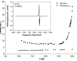
and Mn5Ge3C0.2. The FWHM is presented in figure 6. For the carbon free
235
system (x = 0) at room temperature, the linewidth is large but quickly decreases when decreasing the temperature and reaches an almost constant value of about 7.5 mT when T < 270 K. This is due to the phase transition of Mn5Ge3 from
the paramagnetic phase to the ferromagnetic one at RT. The fluctuation of the magnetization while crossing Tc dramatically increase the linewidth. For
240
Mn5Ge3C0.2, the Curie temperature is much higher with a value estimated at
about 399 K and has no effect on the linewidth in the range of temperature we probed. FWHM is stable, decreasing from 3.5 mT at room temperature down to 2.5 mT at 100 K.
The linewidth of the FMR uniform mode is directly related to the intrinsic
245
quality of the sample. It reflects the intrinsic magnetic damping (homogeneous
Figure 5: (colour online) Normalized magnetization versus temperature for Mn5Ge3 and
Mn5Ge3C0.2samples grown by RDE (applied field H=1.0 T) and for Mn5Ge3Cx samples
(x=0, 0.25, 0.6) grown by SPE (data from fig.2 [29]). Inset: Normalized magnetization versus T/Tcfor the RDE samples.
broadening) and the film inhomogeneities (inhomogeneous broadening) due to a wide variety of parameter variations (film thickness, surface anisotropy, applied field etc.). FMR of Mn5Ge3has been studied in the past [30] showing a linewidth
of many hundreds of mT. The samples grown by SPE do not exhibit clear FMR
250
signal. The sharpness of the FMR linewidth of Mn5Ge3and Mn5Ge3C0.2 grown
using the RDE method is a clear evidence of the high quality of the sample and the great improvement of the growing method.
4. Conclusion
We have demonstrated the reactive deposition epitaxy of Mn5Ge3Cx on
255
Ge(111) substrates at room temperature. Mn5Ge3Cx thin films up to 300 nm
thick were grown. Structural analysis were performed on these films using vari-ous characterization means. The crystallinity was proved to be of good quality with no threading dislocation. The interfaces between the Ge(111) substrates and the Mn5Ge3Cxfilms were atomically sharp and the films surfaces remained
260
measure-Figure 6: Temperature dependence of the FMR full width at half maximum of Mn5Ge3 and
Mn5Ge3C0.2. The magnetic field is set perpendicular to the film and the microwave frequency
was 9.4 GHz. The inset is an example of FMR signal of Mn5Ge3C0.2recorded at 300 K.
ments confirmed the values of the Curie temperature of being similar to those usually found for Mn5Ge3Cxthin films. Moreover very sharp FMR spectra with
a FWHM below 7.5 mT were recorded which is a very significant evidence of the high quality of the thin films grown by our RDE method.
265
Acknowledgements
The authors would like to thank Alain Ranguis for the AFM observations, Mohammad El Zrir, Damien Chaudanson and Serge Nitsche for the TEM prepa-ration and pictures and Cyril Coudreau for the technical support regarding the MBE chambers. The authors thank the interdisciplinary French EPR network
270
RENARD ( CNRS - FR3443). Parts of this work has been carried out thanks to the support of the A*MIDEX project (ANR-11-IDEX-0001-02) funded by the ”Investissements d’Avenir” French Government program, managed by the French National Research Agency (ANR).
References
275
[1] S. A. Wolf, D. D. Awschalom, R. A. Buhrman, J. M. Daughton, S. von Moln´ar, M. L. Roukes, A. Y. Chtchelkanova, D. M. Treger, Spintronics: a spin-based electronics vision for the future., Science (New York, N.Y.) 294 (5546) (2001) 1488–95. doi:http://dx.doi.org/10.1126/science. 1065389.
280
URL http://www.ncbi.nlm.nih.gov/pubmed/11711666
[2] Y. Tawara, K. Sato, On the magnetic anisotropy of single crystal of mn5ge3, Journal of the Physical Society of Japan 18 (6) (1963) 773–777. doi:http: //dx.doi.org/10.1143/JPSJ.18.773.
[3] Y. S. Dedkov, M. Holder, G. Mayer, M. Fonin, A. B.
Preobrajen-285
ski, Spin-resolved photoemission of a ferromagnetic mn5ge3(0001) epilayer on ge(111), Journal of Applied Physics 105 (7) (2009) –. doi:http://dx.doi.org/10.1063/1.3103336.
URL http://scitation.aip.org/content/aip/journal/jap/105/7/ 10.1063/1.3103336
290
[4] C. Zeng, S. C. Erwin, L. C. Feldman, A. P. Li, R. Jin, Y. Song, J. R. Thompson, H. H. Weitering, Epitaxial ferromagnetic mn5ge3 on ge(111), Applied Physics Letters 83 (24) (2003) 5002–5004. doi:http://dx.doi. org/10.1063/1.1633684.
URL http://link.aip.org/link/?APL/83/5002/1
295
[5] S. F. Olive-Mendez, A. Spiesser, L. A. Michez, V. Le Thanh, A. Glachant, J. Derrien, T. Devillers, A. Barski, M. Jamet, Epi-taxial growth of mn5ge3/ge(111) heterostructures for spin in-jection, Thin Solid Films 517 (1) (2008) 191–196. doi:http: //dx.doi.org/10.1016/j.tsf.2008.08.090.
300
URL http://www.sciencedirect.com/science/article/pii/ S0040609008009176
[6] I. Slipukhina, E. Arras, P. Mavropoulos, P. Pochet, Simulation of the enhanced curie temperature in mn5ge3cx compounds, Applied Physics Let-ters 94 (19) (2009) 192505. doi:http://dx.doi.org/10.1063/1.3134482.
305
URL http://link.aip.org/link/APPLAB/v94/i19/p192505/s1&Agg= doihttp://link.aip.org/link/?APL/94/192505/1
[7] J. Tang, C.-Y. Wang, M.-H. Hung, X. Jiang, L.-T. Chang, L. He, P.-H. Liu, H.-J. Yang, H.-Y. Tuan, L.-J. Chen, K. L. Wang, Ferromagnetic germanide in ge nanowire transistors for spintronics application., ACS nano 6 (6)
310
(2012) 5710–7. doi:http://dx.doi.org/10.1021/nn301956m. URL http://www.ncbi.nlm.nih.gov/pubmed/22658951
[8] J. Tang, C.-Y. Wang, L.-T. Chang, Y. Fan, T. Nie, M. Chan, W. Jiang, Y.-T. Chen, H.-J. Yang, H.-Y. Tuan, L.-J. Chen, K. L. Wang, Electrical spin injection and detection in mn5ge3/ge/mn5ge3 nanowire transistors.,
315
Nano letters 13 (9) (2013) 4036–43. doi:http://dx.doi.org/10.1021/ nl401238p.
URL http://www.ncbi.nlm.nih.gov/pubmed/23937588
[9] A. Spiesser, S. Watanabe, H. Saito, S. Yuasa, K. Ando, Effective creation of spin polarization in p-type ge from a fe/geo2 tunnel contact, Japanese
320
Journal of Applied Physics 52 (4S) (2013) 04CM01. doi:http://dx.doi. org/10.7567/JJAP.52.04CM01.
URL http://stacks.iop.org/1347-4065/52/i=4S/a=04CM01
[10] T. Nishimura, O. Nakatsuka, S. Akimoto, W. Takeuchi, S. Zaima, Crystalline orientation dependence of electrical properties of mn
ger-325
manide/ge(111) and (001) schottky contacts, Microelectronic Engineering 88 (5) (2011) 605–609. doi:http://dx.doi.org/10.1016/j.mee.2010. 08.014.
URL http://linkinghub.elsevier.com/retrieve/pii/ S016793171000300X
330
[11] A. Sellai, A. Mesli, M. Petit, V. Le Thanh, D. Taylor, M. Henini, Barrier
height and interface characteristics of au/mn5ge3/ge (1 1 1) schottky contacts for spin injection, Semiconductor Science and Technology 27 (3) (2012) 035014. doi:http://dx.doi.org/10.1088/0268-1242/27/3/ 035014.
335
URL http://stacks.iop.org/0268-1242/27/i=3/a=035014?key= crossref.472100e2753596f2fa58479fdab6460f
[12] G. Scappucci, G. Capellini, W. C. T. Lee, M. Y. Simmons, Ultradense phosphorus in germanium delta-doped layers, Applied Physics Letters 94 (16) (2009) 162106. doi:http://dx.doi.org/10.1063/1.3123391.
340
URL http://scitation.aip.org/content/aip/journal/apl/94/16/ 10.1063/1.3123391
[13] G. Scappucci, G. Capellini, W. M. Klesse, M. Y. Simmons, Phosphorus atomic layer doping of germanium by the stacking of multiple δ layers., Nan-otechnology 22 (37) (2011) 375203. doi:http://dx.doi.org/10.1088/
345
0957-4484/22/37/375203.
URL http://www.ncbi.nlm.nih.gov/pubmed/21857100
[14] A. Spiesser, H. Saito, R. Jansen, S. Yuasa, K. Ando, Large spin accu-mulation voltages in epitaxial mn5ge3 contacts on ge without an oxide tunnel barrier, Physical Review B 90 (20) (2014) 205213. doi:http:
350
//dx.doi.org/10.1103/PhysRevB.90.205213.
URL http://link.aps.org/doi/10.1103/PhysRevB.90.205213
[15] H. R. Lazar, V. Misra, R. S. Johnson, G. Lucovsky, Characteristics of metalorganic remote plasma chemical vapor deposited al2o3 gate stacks on sic metaloxidesemiconductor devices, Applied Physics Letters 79 (7) (2001)
355
973. doi:http://dx.doi.org/10.1063/1.1392973.
URL http://scitation.aip.org/content/aip/journal/apl/79/7/10. 1063/1.1392973
[16] E. Kasper, S. Heim, Challenges of high ge content silicon ger-manium structures, Applied Surface Science 224 (1-4) (2004) 3–8.
doi:http://dx.doi.org/10.1016/j.apsusc.2003.08.022.
URL http://linkinghub.elsevier.com/retrieve/pii/ S016943320301047X
[17] M. Sakuraba, D. Muto, M. Mori, K. Sugawara, J. Murota, Very low-temperature epitaxial growth of silicon and germanium
us-365
ing plasma-assisted cvd, Thin Solid Films 517 (1) (2008) 10–13. doi:http://dx.doi.org/10.1016/j.tsf.2008.08.028.
URL http://linkinghub.elsevier.com/retrieve/pii/ S0040609008008341
[18] R. Ito, M. Sakuraba, J. Murota, Hole tunnelling properties in
370
resonant tunnelling diodes with si/strained si0.8ge0.2 heterostruc-tures grown on si(100) by low-temperature ultraclean lpcvd, Semiconductor Science and Technology 22 (1) (2007) S38–S41. doi:http://dx.doi.org/10.1088/0268-1242/22/1/S09.
URL http://stacks.iop.org/0268-1242/22/i=1/a=S09?key=
375
crossref.0d2afee8703ff1338bcd6c2a5f4b8cd2
[19] M. Yoshimoto, R. Yamauchi, D. Shiojiri, G. Tan, S. Kaneko, A. Mat-suda, Room-temperature synthesis of epitaxial oxide thin films for development of unequilibrium structure and novel electronic functional-ization, Journal of the Ceramic Society of Japan 121 (1409) (2013) 1–9.
380
doi:http://dx.doi.org/10.2109/jcersj2.121.1.
URL http://japanlinkcenter.org/DN/JST.JSTAGE/jcersj2/121.1? lang=en&from=CrossRef&type=abstract
[20] T. Luong, A.Ghrib, M. Dau, M. Zrir, M. Stoffel, V. L. Thanh, R. Daineche, T. Le, V.Heresanu, O. Abbes, M.Petit, M. E. Kurdi, P. Boucaud, H. R.
385
J.Murota, Molecular-beam epitaxial growth of tensile-strained and n-doped ge/si(001) films using a gap decomposition source, Thin Solid Films 557 (2014) 70–75. doi:http://dx.doi.org/10.1016/j.tsf.2013.11.027. [21] C. Zeng, W. Zhu, S. C. Erwin, Z. Zhang, H. H. Weitering, Initial stages of
mn adsorption on ge(111), Physical Review B 70 (205340) (2004) 205340.
390
doi:http://dx.doi.org/10.1103/PhysRevB.70.205340. URL http://link.aps.org/doi/10.1103/PhysRevB.70.205340
[22] A. Nikiforov, B. Kanter, O. Pchelyakov, Rheed investigation of lim-iting thickness epitaxy during low-temperature si-mbe on (100) surface, Thin Solid Films 336 (1-2) (1998) 179–182. doi:http:
395
//dx.doi.org/10.1016/S0040-6090(98)01234-6.
URL http://linkinghub.elsevier.com/retrieve/pii/ S0040609098012346
[23] A. Spiesser, F. Virot, L.-A. Michez, R. Hayn, S. Bertaina, L. Favre, M. Pe-tit, V. Le Thanh, Magnetic anisotropy in epitaxial mn5ge3 films,
Physi-400
cal Review B 86 (3) (2012) 035211. doi:http://dx.doi.org/10.1103/ PhysRevB.86.035211.
URL http://link.aps.org/doi/10.1103/PhysRevB.86.035211
[24] M. Hansen, Constitution of binary alloys, Metallurgy and Metallurgical Engineering Series, McGraw-Hill Book Company, Inc., 1958.
405
[25] O. Abbes, A. Portavoce, V. Le Thanh, C. Girardeaux, L. Michez, Phase formation during mn thin film reaction with ge: Self-aligned germanide process for spintronics, Applied Physics Letters 103 (17) (2013) 172405. doi:http://dx.doi.org/10.1063/1.4827100.
URL http://scitation.aip.org/content/aip/journal/apl/103/17/
410
10.1063/1.4827100
[26] V. Myagkov, V. Zhigalov, a.a. Matsynin, L. Bykova, Y. Mikhlin, G. Bon-darenko, G. Patrin, G. Yurkin, Formation of ferromagnetic germanides by solid-state reactions in 20ge/80mn films, Thin Solid Films 552 (2014) 86–91. doi:http://dx.doi.org/10.1016/j.tsf.2013.12.029.
415
URL http://linkinghub.elsevier.com/retrieve/pii/ S0040609013020920
[27] M. Gajdzik, C. S¨urgers, M. T. Kelemen, H. v. L¨ohneysen, Strongly enhanced curie temperature in carbon-doped mn5ge3 films, Jour-nal of Magnetism and Magnetic Materials 221 (3) (2000) 248–254.
420
doi:http://dx.doi.org/10.1016/S0304-8853(00)00494-7.
URL http://www.sciencedirect.com/science/article/pii/ S0304885300004947
[28] G. Kappel, G. Fischer, A. Jaegle, On the saturation magnetization of mn5ge3, Physics Letters 45 (3) (1973) 267–268. doi:http://dx.doi.org/
425
10.1016/0375-9601(73)90199-0.
[29] A. Spiesser, I. Slipukhina, M.-T. Dau, E. Arras, V. Le Thanh, L. Michez, P. Pochet, H. Saito, S. Yuasa, M. Jamet, J. Derrien, Control of mag-netic properties of epitaxial mn5ge3cx films induced by carbon doping, Physical Review B 84 (2011) 165203. doi:http://dx.doi.org/10.1103/
430
PhysRevB.84.165203.
URL http://link.aps.org/doi/10.1103/PhysRevB.84.165203
[30] M. Terada, M. Sakata, H. Nos´e, Ferromagnetic resonance in thin films of mn5ge3, Journal of the Physical Society of Japan 34 (3) (1973) 619–622. doi:http://dx.doi.org/10.1143/JPSJ.34.619.
435
URL http://dx.doi.org/10.1143/JPSJ.34.619

![Figure 4: a) XRD 2Θ scan of a 300 nm thick film of Mn 5 Ge 3 . b) Zoom of XRD 2Θ scans of Mn 5 Ge 3 and Mn 5 Ge 3 C 0.2 thin films around the Mn 5 Ge 3 [0002] and [0004] peak positions.](https://thumb-eu.123doks.com/thumbv2/123doknet/14660055.739521/12.918.292.630.315.829/figure-xrd-scan-thick-zoom-scans-films-positions.webp)
![Figure 5: (colour online) Normalized magnetization versus temperature for Mn 5 Ge 3 and Mn 5 Ge 3 C 0.2 samples grown by RDE (applied field H=1.0 T) and for Mn 5 Ge 3 C x samples (x=0, 0.25, 0.6) grown by SPE (data from fig.2 [29])](https://thumb-eu.123doks.com/thumbv2/123doknet/14660055.739521/15.918.293.626.193.437/figure-colour-normalized-magnetization-temperature-samples-applied-samples.webp)