HAL Id: hal-01738068
https://hal.archives-ouvertes.fr/hal-01738068
Submitted on 20 Mar 2018HAL is a multi-disciplinary open access archive for the deposit and dissemination of sci-entific research documents, whether they are pub-lished or not. The documents may come from
L’archive ouverte pluridisciplinaire HAL, est destinée au dépôt et à la diffusion de documents scientifiques de niveau recherche, publiés ou non, émanant des établissements d’enseignement et de
Electromechanical switching behavior of individual
molecular complexes of Cu and Ni on NaCl-covered
Cu(111) and Ag(111)
Hermann Walch, Thomas Leoni, Olivier Guillermet, Véronique Langlais,
Andrew Scheuermann, Jacques Bonvoisin, Sebastien Gauthier
To cite this version:
Hermann Walch, Thomas Leoni, Olivier Guillermet, Véronique Langlais, Andrew Scheuermann, et al.. Electromechanical switching behavior of individual molecular complexes of Cu and Ni on NaCl-covered Cu(111) and Ag(111). Physical Review B: Condensed Matter and Materials Physics (1998-2015), American Physical Society, 2012, 86 (7), �10.1103/PhysRevB.86.075423�. �hal-01738068�
Electromechanical switching behavior characterization of
adsorbed single Cu- and Ni- molecular complexes
Hermann Walch
1, Thomas Leoni
1, Olivier Guillermet
1, Véronique Langlais
1,
Andrew Scheuermann
1, 2, Jacques Bonvoisin
1and Sébastien Gauthier
1**Corresponding author: gauthier@cemes.fr, tel. +33 5 62 25 79 80, fax. +33 5 62 25 79 99
1. CEMES, CNRS UPR 8011 et Université de Toulouse, 29 rue Jeanne Marvig, 31055 Toulouse, France
Abstract
In a combined Scanning Tunnelling Microscopy (STM) and non-contact Atomic Force Microscopy (nc-AFM) study, we characterize the reversible switching between two stable states of an organometallic complex, namely bis-dibenzoylmethanato-copper (Cu(dbm)2) adsorbed on an insulating thin film. The switching is due to the transfer of
an electron between the STM tip and the molecule, accompanied by a conformational change, i.e. a transition from a square-planar to a tetrahedral geometry. Evidence is given by STM topography and spectroscopy and nc-AFM electrostatic force measurements. Similar experiments conducted on bis-dibenzoylmethanato-nickel (Ni(dbm)2) show that this complex does not switch under comparable experimental
conditions. We discuss these findings within the framework of crystal field theory stating that the occupation of the d-orbitals determines the favored coordination geometry of a complex. Accordingly, only the copper complex can undergo a conformational change that facilitates stable storing of the additional electron.
1. Introduction
Switching single molecules reversibly and in a controlled manner is considered as a major goal for future nanotechnological applications [1-4]. Recently, a wide variety of molecular switches have been characterized by different techniques, in particular by STM [5-14]. Most of the reported work in this field can be coarsely organized around two families of switchable molecules [5]. In the first one, the structure of the molecule changes by isomerization [6]. One of the most prominent examples in that respect is provided by photoisomerizable molecules such as azobenzene and its derivatives [7-9]. In the second one, different charge states of a molecule (coupled to a more or less important conformation change) are used. Single metallic atoms adsorbed on a thin insulating film [10] constitute a limiting case of this category. Organometallic complexes, which basically consist of a central metal ion coordinated with a set of ligands, also belong to this second family. They offer the possibility of being stable in different redox states that are intrinsically coupled to the spatial arrangement of their ligands. These properties have been studied in great detail in coordination chemistry, mostly for molecules in solution [15].
In this paper, we characterize two such coordination compounds by STM and nc-AFM. One of them exhibits perfect reversible switching behavior induced by the capture or the release of an electron, whereas the other one does not. In a qualitative way, these findings can be understood by applying crystal field theory at the single molecule level. This theory, developed by Hans Bethe and John Hasbrouck van Vleck in the 1930s, could explain magnetic and spectroscopic properties of transition metal complexes. Therein, symmetry arguments are used to simplify the quantum mechanical problem of a central transition metal ion located in the non-spherical electrostatic field created by a set of ligands [16]. As a consequence of the reduced symmetry of the ligand field, degenerate d orbitals of the isolated
When molecules are deposited on surfaces, as in this study, their properties may change drastically. Especially on metal surfaces, it is difficult to relate the electronic properties of the adsorbed molecule to those of the gas phase molecule because of the molecular levels broadening and splitting due to their coupling with the electrons of the metal. However, these effects can be limited by using an ultrathin insulating film adsorbed on a metal surface to decouple the molecules from the surface. This decoupling not only allows the application of STM, but also simplifies its interpretation. The theoretical concepts developed for isolated molecules can then be taken as a basis for measurement analysis. Recently, we have reported on the reversible transfer of a single electron to a Cu(II) complex allowing the control of the charge state and the conformation of this molecule, which can be then considered as a molecular switch [14]. In the present work, firstly, the results and main conclusion on the Cu(II) complex are discussed in more details. Then STM measurements obtained on another complex, where Cu has been replaced by Ni are presented. The results for both molecules are compared and discussed within the framework of crystal field theory.
2. Experimental details
The samples were prepared and characterized in ultrahigh-vacuum with a base pressure below 10-10 mbar. The Cu(111) and Ag(111) single crystal was cleaned by several cycles of Ar+ ion sputtering (600 eV) and subsequent annealing at 500°C. Once the surfaces were clean, NaCl bilayers covering approximately 20 percent of the surface were grown onto the substrate held at 50°C. Afterwards, the molecules were thermally deposited directly onto the cooled samples in the LT STM, a modified Omicron STM equipped with a tuning fork of the qPlus sensor type allowing non-contact atomic force microscopy and electrostatic force measurements. The resonance frequency of the tuning forks used in this study was on the order of 25 kHz and their quality factor was in the range 10000-20000. They were equipped with a glued electrochemically etched tungsten tip allowing the simultaneously measurements of tunneling currents and frequency shifts. Control electronics were provided by SPECS. All images, spectra, and manipulation experiments were performed at a temperature of 5K.
The independence between force and current measurements in combined STM and AFM studies has been questioned recently [17,18]. The tunneling current can influence the measurement of the force for two different types of reasons: (1) the instrument can suffer from material limitations. The qPlus sensor being a purely electrical sensor, capacitive cross-talk between the tunneling current and the force signal is very difficult to eliminate totally, as discussed in ref. 17. (2) A fundamental limitation appears on resistive samples. The current-induced potential drop in the sample generates an electrostatic "phantom" force, as analyzed in ref. 18. In both cases, these couplings appear only for large and/or fast varying tunneling currents. In the work reported here, only very low tunneling current were used, below 1 pA when imaging on NaCl bilayers and below 60 pA for the spectroscopic measurements. In addition, rapid bias voltage changes were avoided, as they induce capacitive currents that can perturb the force measurements. For instance, the time scale for the spectra displayed in figure 4 was on the order of 1 minute. Finally, these coupling effects are expected to make the ∆f(V) spectrum deviate from their expected parabolic behavior, which is not the case as will be
underlined below. For these reasons, we consider that our measurements are free from any tunneling current-force coupling.
Another critical aspect of the experiments reported here concerns the tip characterization. Before performing the spectroscopic measurements, we insured that the following criteria were met. The tip was prepared on a Cu(111) area of the substrate until it displayed a good molecular resolution and an I(V) spectrum showing metallic behavior (finite conductance around 0 bias). We also required that the constant-current ∆f map showed sharp features on molecules, without shadow images due to multiple tip effects.
The syntheses of the two coordination complexes studied here are described elsewhere [19, 20]. Unlike Cu(dbm)2, Ni(dbm)2 crystal was found by X ray diffraction experiments to have a
distorted octahedral geometry due to the integration of the solvent tetrahydrofuran (THF) in the molecular structure. Nevertheless, thermogravimetric analysis showed that the two THF ligands detach at a temperature considerably lower than the sublimation temperature. Hence, pure Ni(dbm)2 can be evaporated after degassing procedures at sufficiently high temperatures.
3. Cu(dbm)2 – a single molecular redox switch
3.1Switching by STM
In a recent study, we introduced the reversible molecular redox switch Cu(dbm)2 [14]. The
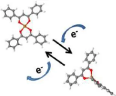
molecule consists of a central Cu2+ ion coordinated with two negatively charged dibenzolylmethane (dbm) ligands. Our results showed that the molecule can be reversibly switched between two stable states from a neutral square planar (SP) to a negatively charged tetrahedral (Td) state[14] as sketched in figure 1.
Figure 1. Molecular models of Cu(dbm)2 in its neutral and charged configuration.
After thermal evaporation, the molecules adsorb in their neutral state in the SP geometry. Since surface diffusion is sufficiently low at 5K, molecules are present both on the NaCl bilayer and on the metallic support. An STM image of Cu(dbm)2 molecules on Cu(111) is
shown in figure 2. The twofold symmetry corresponding to the model in figure 1 can be identified. Some molecules exhibit also a slight distortion of their ligands that can be attributed to an enhanced interaction with specific sites of the metal substrate in contrast to the adsorption on NaCl where no such distorted species are found.
Figure 2. Constant-current STM image of Cu(dbm)2 molecules adsorbed on Cu(111). It= 5pA, Ut = 200 mV.
A typical STM manipulation experiment demonstrating the switch is presented as a series of STM images in figure 3. Four Cu(dbm)2 molecules adsorbed on a bilayer of NaCl on Cu(111)
are labeled in figure 3(a.). One by one, the molecules are switched from the SP to the Td state by applying a voltage pulse of +2V above the center of the molecule (figure 3(e)). A single molecule can be precisely addressed with the STM tip without disturbing its neighbors as it can be seen by the switching events in figure 3(c) to 3(e). In figure 3(c), the STM tip was located above the center of molecule 3 and a voltage pulse was applied resulting in the switching of molecule 3 while molecule 4, located very close remains unaffected. Only when performing the switching procedure above the center of molecule 4, is the transition achieved, as shown in figure 3(e).
The reversibility of the switches is demonstrated in figure 3(e)-(i). Here, applying a voltage pulse of opposite sign on the top of each molecule, i.e. -2 V, restores their initial SP state, as shown in figure 3(i). Note that the remarkable spatial selectivity of the SP to Td transition is maintained for the reverse Td to SP transition, as demonstrated in figure 3(g)-(i). Comparing figure 3(a) with figure 3(i), it can be seen that molecules 1 and 3 have undergone a small rotation. Moreover, similar experiments were performed on a 2-monolayer thick NaCl film deposited on Ag(111) with the Cu(II) complex yielding comparable results, and thus, indicating that the metal substrate does not have a major influence on the switching mechanism.
3.2Charge detection by nc-AFM
Information on the charge state of a species adsorbed on a thin insulating film can be extracted from STM measurements [10,11,13,21]. But a more direct method, based on the measurement of the tip-sample electrostatic force, is provided by nc-AFM [22,23].
Tip-sample electrostatic forces can be distinguished from other forces (van der Waals or chemical forces for instance) by their quadratic dependence on the applied bias voltage. The bias voltage for which the electrostatic force is minimal gives the local contact potential difference (LCPD), the quantity that is mapped with Kelvin Force Probe Microscopy (KPFM), a technique that was implemented with AFM since 1991 [24].
Figure 3. Series of STM images showing the controlled switching transition of the Cu(dbm)2
complex from SP to Td state (from a to e) and the reversible transition from Td to SP state (from f to i). It = 400 fA, Ut = 100 mV. Z scale = 0.28 nm.
In nc-AFM, this quadratic dependence is maintained for the contribution of the electrostatic forces to the resonance frequency shift ∆f. Hence, a constant-height measurement of ∆f as a function of the bias voltage V should give a parabola. Note that this is true only if changes in the structure of the system, such as molecular relaxation or change of conformation do not happen while V is varied. In a simple model, the electrostatic force in the presence of a charge q in the tunnelling junction includes three terms: (1) A purely capacitive term proportional to (V-Vcpd)2 and independent of q. Here Vcpd is the bias voltage that minimizes the electrostatic
force (and consequently maximizes ∆f) when the tip is positioned on the NaCl/Cu(111) substrate, far from any molecule or defect. (2) A term proportional to q2 that describes the interaction of q with its surroundings in the absence of bias. (3) A term proportional to q(V-Vcpd) that originates from the interaction of q with the electric field associated with the bias V
[25,26]. It is this last term that is used to distinguish the sign of the charge q in our measurements as it is responsible for the lateral shift of the maximum of the parabola in a direction that depends on the sign of q. In practise, it has been established that a negative charge induces a shift towards higher voltage [25,26].
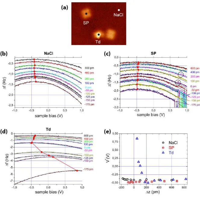
Three sets of ∆f(V) curves acquired on the NaCl substrate, a SP and a Td species, are displayed in figure 4. For each of the curves, the tip was positionned in one of the positions indicated in figure 4(a) while in the constant tunnelling current mode. The distance-controlled loop was then disabled and the tip vertically displaced by the amount ∆z, where positive values of ∆z correspond to an increased distance. The bias V was swept from -1V to +1V
Figure 4. (a) STM image of two SP and one Td molecules. The dots indicate the positions
where the ∆f(V) spectra displayed in (b) for the NaCl substrate, in (c) for the SP and in (d) for the Td species have been acquired. It = 700 fA, Vt = 400 mV. The values of ∆z are indicated
on the right of each spectrum. The fitting parabolas are drawn in black and the positions of the maxima of the parabola in red, related by red lines. (e) Values of the voltages V* corresponding to maxima of the parabolas as a function of ∆z for the NaCl substrate, the SP
and the Td species. Oscillation amplitude A = 240 pm.
(forward direction) first, and then from +1V to -1V (backward direction). For the curves of figure 4(b) and (d), the forward and backward curves were identical except for the frequency noise, which is on the order of 100 mHzpp in these measurement conditions. This indicates
that the measurements were not affected by spatial drift or irreversible changes in the molecule-substrate system. Consequently, only the average curves are shown in these two figures. In contrast, small but significant differences can be observed between the forward and backward curves that are shown in figure 4(c). There are observed for biases in the 0.6-0.8 V interval (see for instance the circles drawn in fig. 4(c)). They are associated with a
conformation change of the molecule whose nature is still under study. In the present work, only the left parts of these curves, for which the forward and backward curves are identical except for the frequency noise, were considered.
With these precautions, the curves were unambiguously identified as parabolas and could be precisely fitted to determine their maxima (see the lines and the red dots in figure 4(b), (c) and (d)). The values of the voltages V* corresponding to these maxima are plotted in figure 4 (e) as a function of ∆z for the NaCl substrate, the SP and the Td species. The ∆z scale of this graph has been corrected for the SP and the Td species by adding to it their height measured on the image of figure 4 (a) (0.085 nm for SP and 0.225 nm for Td). In this way, the ∆z scale becomes a common z scale relative to the substrate.
The first observation that can be made on figure 4(e) is that V* stays approximately constant on NaCl. This behaviour is expected, since on a uniform homogeneous substrate V* gives the LCPD, wich does not depend on the distance. V*SP follows approximately the same
behaviour, meaning that SP is neutral. In contrast, there is a significant shift towards higher bias for Td, as compared to the bare NaCl substrate, and SP when the tip is approached to the surface. According to previous reports, this observation indicates that Td is negatively charged. Therefore, we conclude that SP can be described as a neutral molecule [Cu(II)dbm2]0
and Td as a negative ion [Cu(I)dbm2]-1.
We remark that the shift towards higher bias of V* reaches very high values (more than 1V relative to NaCl). Nevertheless, it is comparable with the maximal value reported for negatively charged Au on NaCl/Cu(111), which is nearly 0.5 V. In any case, the values and distance dependence are related to the detailed structure of the tip and cannot be explained by simple models. More realistic calculations are needed to interpret them [27].
The frequency shift ∆f*=∆f(V*) is plotted in figure 5 for the three species characterized in figure 4 as a function of ∆z. For this bias, the electrostatic force is minimized, and only the term that is proportional to q2 contributes, in addition to the ever-present van der Waals interaction. ∆f* remains similar for NaCl and the SP molecule, but deviates significantly toward large negative values for the Td ion, revealing the presence of a large attractive force. Even if it is not possible to determine the respective contributions of these forces without precise calculations, this observation is consistent with the Td species being charged.
Figure 5. Frequency shift at the maximum of the parabola of figure 4 (b), (c), and (d) as a
function of ∆z.
3. Ni(dbm)2 – comparison of the two complexes
For an in-depth understanding of the switching process, STM measurements were performed on a similar complex, where the Cu ion was replaced by a Ni ion. Similarily to Cu(dbm)2,
Ni(dbm)2 was deposited on a bilayer of NaCl on Cu(111) at low temperature. The molecular
structures are identical, differing only by the chemical nature of the central metal ion. For both, the Cu(II) and Ni(II) ions are coordinated with four oxygen atoms bridging four phenyl rings as depicted in the model (figure 1). Using the procedure described above, attempts were carried out to switch the molecules but without success. Applying bias voltages higher than 2V did not change the square-planar appearance of the molecule (figure 6).
Figure 6. STM image of Ni(dbm)2 molecules adsorbed on NaCl/Cu(111). It=400 fA, Ut=600
mV.
I(V) curves were recorded on the three species at hand, namely, the neutral SP Cu(II) complex, the charged Td Cu(I) complex and the neutral SP Ni(II) complex as shown in figure 7. The spectra on the copper complexes (figure 7(a) and (b)) show that the switch i.e. the capture (figure 7(a)) or the loss (figure 7(b)) of the additional electron is related to a jump in the tunneling current at a bias voltage located in the range where the SOMO (Singly Occupied Molecular Orbital) of the complex contributes, with an onset at about +1.8 V. At this energy just below the switching bias, the molecule appears in STM images suddenly blown up, as could be seen in figure 8(a). These features could be attributed to molecular ion resonances as
mentioned in [28,29]. Further on, a sudden drop in the tunneling current takes place indicating the transition to the Td state as STM images reveal after this event. In the negative range (figure 7(a)), no jump corresponding to a resonance is detected, i.e. when imaging with STM, the molecule keeps its SP four lobes aspect. In a parallel way, the curves recorded on the Td charged copper complex present a similar characteristic, shown in figure 7(b). From 2 V to -1.4 V, the curves are monotone until a conductance peak located at -1.7 V, whose onset is at about -1.4 V is met. At this energy, the molecules appear as blown up in STM corresponding to the resonance and then a sudden drop (absolute value) of the tunneling current indicating the transition back to the SP state. For comparison, the I(V) curve recorded on the nickel complex shows a smoother increase of the tunneling current above 1 V which is not followed by an abrupt drop as for Cu(dbm)2, which is the signature of the electron transfer
accompanied by the molecular conformational change. Moreover, even when increasing the bias to more than 2.5 V, no drop of the tunneling current is observed. For energies higher than 2.5 V, the molecules start to move on the surface and no proper spectrum or stable image could be recorded. Figure 8 shows STM images at about 1.8 V for both molecules displaying the molecular orbitals.
Figure 7. Spectroscopic I(V) curves recorded on (a) Cu(II)(dbm)2, (b) Cu(I)(dbm)2 and (c)
Ni(II)(dbm)2 complexes.
To some extent, a qualitative comparison of the I(V) curves with cyclic voltammetry (CV) curves (not shown) can be made. Indeed, the Cu(dbm)2 complex in electrochemistry exhibits
a partial irreversibility due to the rearrangement of its coordination sphere from planar to tetrahedral during the reduction process [30,31]. The curve shows that oxidation does not take place until after the corresponding reduction has already occurred, which means that the Cu(II) ion is first reduced into Cu(I) before being oxidized again into Cu(II). On the other hand, the CV curve of the Ni(dbm)2 complex is flat without any feature under the same
Figure 8. STM images showing the molecular orbitals recorded on (a) a single Cu(dbm)2 at Ut=1.85 V, It=400 fA and on (b) a single Ni(dbm)2 molecule at 1.8V, 800 fA both adsorbed on
a NaCl bilayer grown on Cu(111). Both images are 4x4 nm2 in size.
4. A model based on crystal field theory
Qualitatively, crystal field theory helps to understand the switching of Cu(dbm)2. It has been
successfully applied to characterize the physical properties of organometallic complexes by taking into account the electronic d levels of the metal ion. Whereas for an isolated metal ion the five d levels are degenerate, these levels split up into characteristic patterns in the inhomogeneous electrostatic field of a lattice or as in our case, of the ligands. The d level splitting diagram of a transition metal ion in a tetrahedral and a square-planar ligand field shown in figure 9, is a standard textbook example [32,33] . Since for a neutral copper atom the d-shell is completely filled with 10 electrons ([Ar]3d104s1), the electronic configuration of the metallic ion in the Cu(II) complex is [Ar]3d9. It is then immediately clear from the diagrams of figure 9 that the square-planar symmetry should be favored relative to the tetrahedral one, mainly because of the large energy gain due to the presence of an electron hole in the very energetically unfavorable dx2-y2 orbital. In the negatively charged Cu(I) complex, the metal is [Ar]3d10, the d orbitals are fully occupied and, according to CFT, there is no crystal-field stabilization energy preference for any coordination symmetry. In fact, the structure is then governed by inter-ligands steric and electrostatic effects, which are not taken into account in CFT, and a tetrahedral geometry is adopted to minimize the repulsive interaction between the ligands.
The same arguments applied to Ni(dbm)2 (Ni: [Ar]3d84s2) show that the Ni(II) complex
([Ar]3d8) and a hypothetical negatively charged Ni(I) complex ([Ar]3d9) should remain in the SP conformation because of the stabilizing effect of one or two holes in the dx2-y2 orbital. Then, it can be concluded that charging the Ni complex would not induce a change in the ligand symmetry. Nevertheless, a charging event would be detected in our experiments, even in this situation, especially on the spectroscopic I(V) curves, since it should be accompanied by major changes in the electronic structure of the complex. As the curve presented in figure 7 for the Ni complex does not present any feature which could be associated with such a change, we conclude that charging Ni(dbm)2 is not possible in our experimental situation.
Figure 9. Splitting diagrams of the d levels in a tetrahedral and a square planar ligand field.
The central copper ion has a formal charge of 2+ which means that there are nine electrons to be distributed over the d-levels. Summing up the energies for nine electrons for both the Td and the SP splitting diagram shows that the crystal field energy of the SP state is lower than
that of the Td state.
Note that CFT does not permit prediction of the stability of neutral species with respect to the charged ones. Adding or removing a charge to the complex involves multi-electronic effects that are not included in this model. The key question is whether an energy barrier between the neutral and the charged species exists. This is discussed in [34] for Au and Ag adsorbed on NaCl/Cu(111). The discussion involves the electron affinity of the neutral species A, the work function φ, the electronic and ionic relaxation energies, ∆el and ∆ion, where ∆el is associated to
the electronic response of NaCl and the metals (in particular it includes the image charge potential) and ∆ion includes the relaxation energy associated with the static dielectric constant
of NaCl. In the case of the copper complex, the relaxation energy associated with the ligands should also be taken into account in ∆ion. Refined calculations are necessary to answer this
question. Nevertheless, it is clear that the rearrangement of the ligands around the central copper ion plays a major role in the charge stabilization. In contrast for the Ni complex, the absence of an important conformation change is clearly related to the fact that it does not accept an extra electron. Other hints towards these conclusions are brought from the electrochemistry experiments already mentioned, and the fact that there exist numerous organometallic complexes of Cu(I), Cu(II) and of Ni(II) but very few of Ni(I).
5. Conclusions
In summary, we presented the reversible switching between two stable states of a copper complex adsorbed on a bilayer of NaCl on Cu(111) and Ag(111). This transition is triggered by the capture or release of an electron from the molecule. STM topography and spectroscopy and nc-AFM electrostatic force measurements were performed to characterize conformational and charge state. Replacing Cu by Ni in these complexes renders the switching impossible. This finding is in agreement with what is known from the studies of these complexes in solution. It is also in line with the qualitative arguments provided by crystal field theory. The fact that these molecular properties survive adsorption on a solid substrate is a consequence of the electronic decoupling from the metallic substrate brought by the NaCl bilayer. This is also
effect [28,29]. Nevertheless, it should be stressed that the role played by the NaCl layer is less important in the present case than when investigating the switching behavior of an atom adsorbed on the same substrate (NaCl bilayer/Cu(111)) as performed recently for Au [10,22]. In these studies, the NaCl layer not only electronically decouples the species from the metallic substrate, but its ionic relaxation also plays a major role in the charge trapping. In a way, it assumes the role played by the ligands in the molecular complexes that are under study here. We expect that these conclusions will be confirmed by detailed calculations, which are obviously needed to reach a full understanding of these systems.
Acknowledgements
This work was in part supported by World Premier International Research Center (WPI) Initiative on Materials Nanoarchitectonics, MEXT, Japan and by the European Commission within the project ARTIST (Contract No. 343421). A.S. gratefully acknowledges financial support from the NSF Chemistry REU program. The images have been processed with the WSXM software [35].
References
[1] C .Joachim, J. Gimzewski and A. Aviram, Nature 408, 541 (2000).
[2] J. E.Green, J. W. Choi, A. Boukai, Y. Bunimovich, E. Johnston-Halperin, E. DeIonno, Y. Luo, B. A. Sheriff, .K Xu, Y. S. Shin, H.-R. Tseng, J. F. Stoddart and J. R. Heath, Nature 445, 414 (2007).
[3] C. P. Collier, E. W. Wong, M. Belohradsky, F. M. Raymo, J. F. Stoddart, P. J. Kuekes, R. S. Williams, J. R. Heath, Science 285, 391 (1999).
[4] A. Livoreil, C. O. Dietrich-Buchecker and J.-P. Sauvage, J. Am. Chem. Soc. 116, 9399 (1994).
[5] S. Jan van der Molden and P. Liljeroth, J. Phys.: Condens. Matter 22, 133001 (2010). [6] K. Morgenstern, Prog. Surf. Science 86, 115 (2011).
[7] B.-Y. Choi, S.-J. Kahng, S. Kim, H. Kim, H. W. Kim, Y. J. Song, J. Ihm, and Y.
Kuk, Phys. Rev. Lett. 96, 156106 (2006).
[8] C. Dri, M. V. Peters, J. Schwarz, S. Hecht and L. Grill, Nature Nanotech. 3, 649 (2008). [9] A. Safiei, J. Henzl and K. Morgenstern, Phys. Rev. Lett. 104, 216102 (2010).
[10] J. Repp, G. Meyer, F. E. Olsson, M. Persson, Science 305, 493 (2004).
[11] G. Mikaelian, N. Ogawa, X. W. Tu and W. Ho, J. Chem. Phys. 125, 131101 (2006). [12] F. Mohn, J. Repp, L. Gross, G. Meyer, M. S. Dyer, and M. Persson, Phys. Rev. Lett. 105 266102 (2010).
[14] T. Leoni, O. Guillermet, H. Walch, V. Langlais, A. Scheuermann, J. Bonvoisin and S. Gauthier, Phys. Rev. Lett. 106, 216103 (2011).
[15] D. B. Rorabacher, Chem. Rev. 104, 651 (2004). [16] H. Bethe, Ann. Phys. 5, 133 (1929).
[17] Z. Majzik, M. Setvín, A. Bettac, A. Feltz, V. Cháb and P Jelínek, Beilstein J. Nanotechnol. 3 249 (2012).
[18] A. J. Weymouth, T. Wutscher, J. Welker, T. Hofmann and F. J. Giessibl, Phys. Rev. Lett.
106, 226801 (2011).
[19] B.-Q. Ma, S. Gao, Z.-M. Wang, C.-S. Liao, C.-H. Yan and G.-X. Xu J. Chem. Cryst. 29, 793 (1999)
[20] V. Soldatov, A. T. Henegouwen, G. D. Enright, C. I. Ratcliffe and J. A. Ripmeester, Inorg. Chem. 40, 1626 (2001).
[21] J. Repp, G. Meyer, S. Paavilainen, F. E. Olsson, M. Persson, Phys. Rev. Lett. 95, 225503 (2005).
[22] L. Gross, F. Mohn, P. Liljeroth, J. Repp, F. J. Giessibl, G. Meyer G, Science 324, 1428 (2009).
[23] T. König T et al., J. Am. Chem. Soc. 131, 17544 (2009).
[24] M. Nonnenmacher, O. M. P. Boyle and H. K. Wickramasinghe, Appl. Phys. Lett. 58, 2921 (1991).
[25] R. Stomp, Y. Miyahara, S. Schaer, Q. Sun, H. Guo, P. Grutter, S. Studenikin, P. Poole, and A. Sachrajda, Phys. Rev. Lett. 94, 056802 (2005).
[26] Y. Azuma, M. Kanehara, T. Teranishi, Y. Majima, Phys. Rev. Lett. 96, 016108 (2006). [27] F. Bocquet, L. Nony and C. Loppacher, Phys. Rev. B 83 035411 (2011).
[28] J. Repp, G. Meyer, S. Stojkovic´, A. Gourdon and C. Joachim, Phys. Rev. Lett. 94, 026803 (2005).
[29] C. V. Villagomez, T. Zambelli, S. Gauthier, A. Gourdon, C. Barthes, S. Stojkovic´ and C. Joachim, Chem. Phys. Lett. 450, 107 (2007).
[30] V. Amendola, L. Fabbrizzi, L. Linati, C. Mangano, P. Pallavicini, V. Pedrazzini V and M. Zema, Chem. Eur. J. 5, 3679-88 (1999).
[31] J. R. Bradbury, J. L. Hampton, D. P. Martone and A. W. Maverick, Inorg. Chem. 28, 2392 (1989).
[34] F. E. Olsson, S. Paavilainen, M. Persson, J. Repp and G. Meyer, Phys. Rev. Lett. 98, 176803 (2007).
[35] I. Horcas, R. Fernández, J. M. Gómez-Rodríguez, J. Colchero, J. Gómez-Herrero and A. M. Baro, Rev. Sci. Instrum. 78, 013705 (2007).