(SrTiO
3) single crystal
Dong Su, Anna Infortuna, Paul Muralt, and Nava Settera)
Ceramics Laboratory, Swiss Federal Institute of Technology (EPFL), Lausanne CH-1015, Switzerland Marco Cantoni
Interdisciplinary Center for Electron Microscopy (CIME), Swiss Federal Institute of Technology (EPFL), Lausanne CH-1015, Switzerland
(Received 18 April 2006; accepted 25 September 2006)
Strontium barium niobate (Sr2.5Ba2.5Nb10O30) thin films were deposited on (001)
SrTiO3single-crystalline substrates by pulsed laser deposition. The growth nature was
investigated by transmission electron microscopy (TEM). Selected-area electron diffraction and high-resolution transmission electron microscopy revealed the existence of six types of grains. These grains grew on the substrate in a partially epitaxial fashion. Geometrical models were built, which were confirmed by TEM observations. Based on the TEM results and geometrical analysis, a crystallographic model was developed. The strain nature resulting from the growth columns is discussed in this report.
I. INTRODUCTION
The tungsten-bronze (TB) structure strontium barium niobate (Sr5xBa5−5xNb10O30, SBNx) is a uniaxial
ferro-electric at room temperature, and its monocrystals exhibit large piezoelectric, pyroelectric, and electro-optic coef-ficients.1,2The para-to-ferroelectric phase transition oc-curs in the temperature range from 333 to 523 K, de-pending on the compositional parameter x. The large spontaneous polarization along the unique c axis leads to a very strong dielectric anomaly. The relatively low criti-cal temperature of SBNxmakes it an excellent candidate
for pyroelectric infrared detectors. In view of these ex-cellent single-crystal properties, there is an interest in investigating SBN thin films for applications in electro-mechanical and optical microsystem.3
In this work, epitaxial growth of SBNx thin films is
investigated. Currently, there is no commonly available TB crystalline substrate. The most commonly used sub-strates are (001) oriented perovskite single crystals, such as MgO (NaCl-tpye structure) and SrTiO3, because they
have very low lattice mismatch along the c axis of SBNx.
4–8
Thus, the interesting question arises: How is the TB structure accommodated on (001) perov-skites? Growth of SBNx⳱0.56 and SBNx⳱0.61 on (100)
MgO single crystals was studied by Thony et al. and
C.M. Rouleau et al., respectively.6,7 Their results show the growth relationship to be SBNx〈100〉//MgO〈310〉.
Tanaka and co-workers reported the same growth rela-tionship SBNx〈100〉//STO〈310〉 in SBNx⳱0.5thin film on
(001) STO single crystal.8They also indicated that in the configuration of SBNx〈100〉//STO〈310〉, the lattice
mis-match calculated is less than 1%, while the mismis-match for SBNx〈100〉//MgO〈310〉 is −6.2%. STO is a more suitable
substrate for SBN epitaxial growth because it has a smaller misfit strain than MgO. Although a growth rela-tion of SBN〈100〉//MgO〈310〉 was reported in their work, the growth nature of a TB-type SBN on perovskite sub-strate is still unclear.
In this work, we deposited epitaxial SBNx⳱0.5(SBN50,
SBN hereafter) thin films on (100) SrTiO3(STO) single
crystals by pulsed laser deposition (PLD). The growth nature was investigated by transmission electron micros-copy (TEM). According to the lattice parameters’ rela-tionship between SBN and STO, the growth models were built. By diffraction simulating, we were able to compare the TEM results and the prediction of our models. The growth mechanism was discussed in terms of the lattice-mismatch strain between the film and the substrate.
II. EXPERIMENTAL PROCEDURE
SBN thin films were deposited on (001) STO sub-strates by PLD with a KrF excimer laser ( ⳱ 248 nm). The targets were prepared by mixing SrCO3, BaCO3, and
Nb2O5 powders in acetone and calcined at 1373 K for
a)
Address all correspondence to this author. e-mail: [email protected]
12 h in air. The deposition temperature was 1013 K in oxygen atmosphere of 200–400 mTorr. The laser energy and repetition rate were 200–400 mJ and 10 Hz, respec-tively. Atomic steps for SrTiO3 (1% Nb doped)
sub-strates were observed via atomic force microscopy (AFM) prior to deposition. The crystallization of SBN thin films was examined by reflection high-energy elec-tron diffraction (RHEED), which showed a high degree of roughness on the film surface. The detailed experi-mental procedure can be found elsewhere.9
Cross-section samples of SBN thin films were cut along the [100] direction of STO. The cut slides were glued face to face by jointing SBN film surfaces. TEM specimens were prepared by mechanical grinding, pol-ishing down to 25m, followed by Ar-ion milling with a Gatan-PIPS (Pleasanton, CA). Plane-view samples were prepared by similar methods from the substrate side. The conventional diffraction contrast images and diffraction patterns were obtained in a Philips CM20 TEM (Hillsboro, OR). High-resolution transmission electron microscopy (HRTEM) was taken using a CM-300 FEG TEM.
III. RESULTS AND DISCUSSION A. Growth models
At room temperature, the unit cell lattice parameters are a⳱ b ⳱ 1.246 nm and c ⳱ 0.3952 nm for SBN (No. 39-0265 in the Powder Diffraction File database) and a⳱ b ⳱ c ⳱ 0.3905 nm for STO (No. 79-0174).10,11It can be seen that the value of cSBNis close to the value of
aSTO, which means that it is possible for SBN to grow
epitaxially on STO substrate. On the other hand, the value of aSBNis much larger than the value of aSTO. This
arrangement would lead to growth of SBN on STO that is not completely epitaxial, unlike cube-on-cube growth in system of perovskite on perovskite. The relationships between lattice parameters of SBN and STO are:
|aSTO| ≈ |cSBN| , (1) 共|aSTO|兲 2 + 共3|a STO|兲 2≈ 共|a SBN|兲 2 . (2)
To minimize the interface energy, the lattice of the SBN film would have the maximum match with the STO substrate on the growth. Therefore, from a geometrical view, six types of possible growth models can be de-duced. The relationships of the lattice vectors are as fol-lows:
Model 1: cSBN ≈ aSTO, and (3|bSTO|) 2
+ (|cSTO|) 2
≈ (|aSBN|) 2
Model 2: cSBN ≈ aSTO, and (|bSTO|) 2
+ (3|cSTO|) 2
≈ (|aSBN|) 2
Model 3: cSBN ≈ bSTO, and (3|aSTO|) 2
+ (|cSTO|) 2
≈ (|aSBN|) 2
Model 4: cSBN ≈ bSTO, and (|aSTO|) 2
+ (3|cSTO|) 2
≈ (|aSBN|) 2
Model 5: cSBN ≈ cSTO, and (3|aSTO|) 2
+ ( |bSTO|) 2
≈ (|aSBN|) 2
Model 6: cSBN ≈ cSTO, and (|aSTO|) 2
+ (3 |bSTO|) 2
≈ (|aSBN|) 2
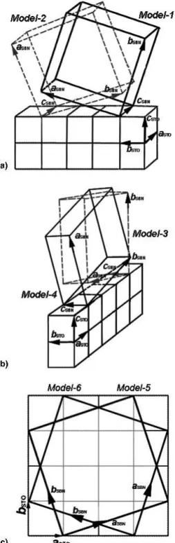
The illustrations of these models are shown in Figs. 1(a)–1(c). In models 1–4, the c axis of SBN grows along the a or b axis of STO, and at the same time, the a or b axis of SBN tilts 18.4° away from the interface of the SBN and STO. In models 5 and 6, the c axis of SBN grows along the c axis of STO, and the a or b axis of SBN tilts in-plane 18.4° away from the a axis of STO. This means SBN grows on STO in the manner of a unit cell match. Other than the cube-on-cube growth in perovskite, these growths are a kind of partially epitaxial growth. An eigen angle, 18.4° [arctg(1/3)], between aSBN
and aSTOis found in all models. The angle 18.4° can be
calculated from relationship (2). This rotation angle re-sults from the tilting between the octahedra in SBN and the vectors of the SBN unit cell. We note that a model similar to models 5 and 6 have been reported in Ref. 6–8. In the following section, we will compare the TEM re-sults with our models.
B. Experimental results
Figure 2 shows the x-ray diffraction (XRD) pattern of SBN thin films on STO single crystals. Splitting can be seen in SBN (001) and SBN (002) peaks, which results from the overlap of SBN (001) and (002) peaks with (310) and (620) peaks, respectively. This result is in agreement with our models, in which the [001] and [130]/[310] zone axes are perpendicular to the film.
A bright-field image of a cross-section SBN film is shown in Fig. 3, which is taken near the [100] axis of STO substrate. Columnar grain structure is observed. In-side the grains, misfit dislocations and a few of threading dislocations are seen. Figure 4(a) shows a selected area diffraction (SAED) pattern from an area including one column and a part of substrate. It is indicated that the STO [100] zone axis accounts for the strong spots, and another pattern is from SBN [001] zone axis, which has a 18.4° rotation from STO [100]. Figure 4(b) is the pat-tern calculated by means the program JEMS based on model 1, which corresponds well with Fig. 4(a).12 Figure 4(c) shows a SAED pattern taken on two grains as well as the substrate. Figure 4(c) includes two series of SBN [001] diffraction patterns, which indicate these two neighbor grains grow with the 〈100〉 zone axis rotated ±18.4° from the STO [100] zone-axis, as indicated in models 1 and 2, respectively.
The SAED pattern from another grain and substrate is shown in Fig. 5(a). Other than the STO [100] zone axis, it presents a [130] zone diffraction pattern of SBN as well
as weak incommensurate superlattice reflections in plane (0, 0, h+1/2). Figure 5(b) is taken from both this grain and the adjacent grain. Besides the SBN [130] (or [310]) zone-axis pattern, both the incommensurate superlattice reflections and vertical SBN [3¯10] (or [13¯0]) zone-axis pattern are observed. A corresponding schematic repre-sentation is shown in Fig. 5(c), where three sets of pat-terns in Fig. 5(b) are represented. First, the strong spots identical in Figs. 5(a) and 5(b) result from the grain with SBN [310] (or [130]) parallel with STO [001], indicated by filled circles. As simulated by JEMS, the (3k, −k, h) type spots are from reflections of the zero Laue-zone, and the (3k±1, −k, h) type spots are from reflections of the first Laue-zone. These spots indicate grain growth by models 3 and 4. Second, the vertical spots from the SBN [3¯10] (or [13¯0]) zone-axis are from the adjacent grains with SBN[001] parallel to STO [001]. These spots indi-cate grain growth by models 5 and 6. Lastly, the streak-like spots are observed on (0, 0, h+1/2) planes. As re-ported in the literature,13–15 these spots are incommen-surate reflections induced by [NbO6] octahedra tilting. It FIG. 1. Illustrations of the growth geometry of SBN on STO.
(a) Model 1: [001]SBN//[100]STO, and [130]SBN//[001]STOor aSBN
ro-tates −18.4° from bSTO; Model 2: [001]SBN//[100]STO, and [310]SBN//
[001]STOor aSBNrotates (18.4–90°) from bSTO. Models 1 and 2 are
seen along STO [100]. (b) Model 3: [001]SBN//[010]STO, and
[130]SBN//[001]STOor aSBNrotates (18.4°-90°) from aSTO; Model 4:
[001]SBN//[010]STO, and [310]SBN//[001]STOaSBNrotates −18.4° from aSTO. Models 3 and 4 are seen along STO [010]. (c) Model 5:
[001]SBN//[001]STO, and [130]SBN//[010]STO or aSBN rotates +18.4°
from aSTO; Model 6 [seen along STI(001)]: [001]SBN//[001]STO, and
[1¯30]SBN//[010]STOor aSBNrotates −18.4° from aSTO; Models 5 and 6
are seen on STO [001]. (+) indicates clockwise rotation, (−) indicates means counterclockwise rotation.
FIG. 2. XRD pattern of SBN thin film on (001) STO single crystal. SBN (001) and (002) peaks show splittings. The STO(200) peak shows no splitting.
FIG. 3. Bright-field image of SBN thin film on STO substrate (cross-section).
FIG. 4. (a) SAED pattern along STO[100] from a cross-section sample. The lattice units of SBN and STO are marked. (b) Calculated SAED pattern by JEMS. (c) SAED pattern along STO [100] from another area of the cross-section sample.
FIG. 5. (a) Cross-sectional SAED pattern of SBN/STO taken along STO [100]. (b) Cross-sectional SAED pattern from two grains. (c) Corresponding schematic representation of (a) and (b). The spots from the zero and first [130] Laue zones of SBN are respectively marked by large and small filled circles; the spots from adjacent grain are indicated by (×), and the spot-streaks of incommensurate reflec-tions are indicated by (—).
is believed the incommensurate superlattice reflections suggest the SBN thin film is orthorhombic phase instead of tetragonal phase. In fact, the existence of (0, 0, h+1/2) superlattice reflections can help to distinguish the SBN [001] and SBN [130] zone axes, which have very similar diffraction patterns at the zero Laue zone.
Figure 6 is a HRTEM micrograph of a cross-section showing the boundary between two SBN grains. The fast Fourier transformations (FFT) on each grain are the same. The FFT pattern of Fig. 6 is shown in inset, where weak superlattice streaklike spots are observed. There-fore, it can be concluded that the two grains have the orientation relationship [001]SBN//[001]STO.
Conse-quently, this boundary is an inverse (domain) boundary separating the two grains of models 5 and 6.
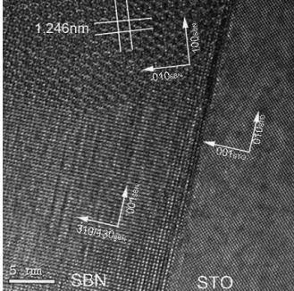
Figure 7 shows a HRTEM image of the film and sub-strate. Two SBN grains are observed with the growth relationships of [001]SBN//[100]STO and [130]SBN
or [310]SBN//[001]STO (model 1 or 2) for grain one
a n d [ 0 0 1 ]S B N/ / [ 0 1 0 ]S T O, a n d [ 1 3 0 ]S B N o r
[310]SBN//[001]STO(model 3 or 4) for grain two.
Addi-tionally, the angle between SBN[100] and STO [010] is measured as 18.4°, which confirms the observation in model 1.
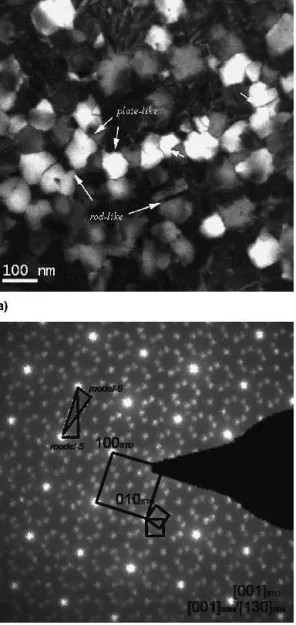
TEM investigations were preformed on plane-view samples. A dark-field image from the plane-view is shown in Fig. 8(a). The STO substrate has been removed by ion milling, and only SBN grains are seen. Therein, two types of grains can be observed; one is platelike (bright), and the other is rodlike (dark). These grains are also seen in AFM observations (not shown). The inverse boundary separating the model 5 grain and the model 6
grain can be observed. Figure 8(b) is the corresponding SAED pattern, in which two series of diffraction patterns correspond to the SBN [001] zone axis and one series of diffraction pattern corresponds to STO [001] zone axis. The patterns of two SBN [001] zone axes are from the planelike grains (models 5 and 6), and they have ±18.4° with the STO [001] zone axis, while the SBN [310]/[130] zone axis from the rodlike grains has the same pattern as STO [001]. These results are in agreement with the XRD pattern shown above, where strong SBN [001] and [130]/ [310] peaks are reported.
With the help of diffraction simulation by JEMS, the grains of models 1–6 were identified by SAED and HRTEM.
C. Crystallographic models and discussion From a crystallographic view, models 1–4 are equiva-lent, as are models 5 and 6. So it is crucial to discuss these six models at the atomic scale. STO is a typical perovskite with Ti in the center of oxygen octahedra (B-site) and Sr at the A site. Comparatively, the unit cell of SBN contains a framework of oxygen octahedral, and the tunnels among them are occupied by Sr and Ba ions. The bonds inside the oxygen octahedron are stable and difficult to break. Therefore, in the growth of SBN on STO, the octahedra structure will be adapted to maintain integrally and become the framework of growth. From the energy point of view, the octahedra of SBN would mainly overlap with the octahedra of STO to reduce the interface energy. According to these analyses and the six geometrical models shown previously, two crystallo-graphic models are developed from the unit models of SBN and STO, as shown in Figs. 9(a) and 9(b), which
FIG. 6. HRTEM image of SBN thin film along the STO [100] zone-axis, showing the boundary of SBN grains. The inset is a FFT of HRTEM image, and the streaklike spots (0, 0, h+1/2) are marked with arrows.
FIG. 7. HRTEM image of SBN thin film along STO [100] zone-axis showing the interface between SBN and STO.
account for models 1–4 and models 5 and 6, respectively. One SBN unit cell has 10 octahedra on the boundary (shared with the neighboring unit cell) and 4 octahedra in the center. There is a relative rotation between them. Therefore, the maximal overlapping of octahedra be-tween film and substrate can be achieved through two possible ways while keeping the growth epitaxial: In the case of Fig. 9(a), 4 oxygen octahedra on one side of the SBN unit cell boundary overlap maximally with the oc-tahedra of the STO substrate. Figure 9(b) shows another case where the 4 octahedra in the center overlap maxi-mally with the octahedra of STO.
From the growth models, it is indicated in Fig. 9(a) that growth has a different mismatch nature along the two directions on the interface between SBN and STO. The strains are 1.2% along aSTOand 0.9% along bSTO. In the
growth shown in Fig. 9(b), the strains are 0.9% along both aSTOand bSTO. [As mentioned above, at room
tem-perature, the unit cell of SBNx⳱0.5should be an
orthorhom-bic cell instead of the tetragonal cell that we used here. However, due to the lack of the knowledge on how the SBN slabs array (see Refs. 13 and 14), it is difficult to determine the realistic strain between the SBN and SBN. What we show here can be considered a reasonable es-timation on the strain at high temperature.] The differ-ence between strains along a and b directions is very small, which makes the different types of grains possible under the growth condition. The existence of dislocations can further relax strain in thin films and thus benefit the epitaxial growth of SBN film on STO single crystals.
Our models are based on the lattice parameters rela-tionship between the SBN and STO. However, these
FIG. 8. (a) Dark-field image from plane-view SBN thin film; (b) corresponding SAED pattern of (a).
FIG. 9. Schematic graphs for SBN crystallographic growth on STO: (a) out-of-plane 18.4° rotation from STO and (b) in-plane 18.4° rota-tion from STO.
quasi-epitaxial models are not limited to these two par-ticular materials, and these models can be applied to the epitaxial growth of tungsten-bronze thin film on other perovskite single crystal, such as MgO and LaAlO3,
within the tolerance of epitaxial growth. Most recently, Jia et al. studied the growth of another TB-type material Ca1.4Ba3.6Nb10O30 (Ca0.28Ba0.72Nb2O6 in their paper;
CBN) on STO single crystals using an advanced negative Cs imaging technique.16
The same growth patterns were found in the CBN/STO system, though the lattice mis-matches in CBN/STO are 0.83% along a axes and 1.58% along c axes. Normally, the strain in thin film formed by PLD is strongly affected by various factors such as oxy-gen pressure, substrate temperature, pulse energy, quality of target, and film thickness. Therefore the growth nature of thin film is also affected. For example, the change of oxygen pressure can lead to the epitaxial growth of perovskite thin film varying from Frank–van Merwe (FM) (layer-by-layer) type to Volmer–Weber (VW) type. The identical models in SBN/STO and CBN/STO sug-gest that our current model is applicable to different stress state. We expect that the same growth model also works in SBN ceramics to reduce the internal strain.
We found that various conditions of surface treating to substrate can also affect the actual growth nature by changing the growth energy.17 Other than the lattice-mismatch strain, the properties of the interface also play an important role in the epitaxial growth. This can be understood within the frame of the coincident site lattice approaches16,18
; the surface treating can definitely influ-ence the distribution of the atoms on the surface and lead to a change in the surface energy. In this case, an energy-favorable model will dominate the growth.
IV. CONCLUSIONS
In summary, TB-type SBN thin films were deposited on (001) SrTiO3 single crystals. Based on relationships
of the lattice parameters, six geometrical models of growth were built and a 18.4° rotation between film and substrate was found as a characteristic of this partially epitaxial growth. These results were confirmed by TEM. A kind of incommensurate superlattice reflection on (0, 0, h+1/2) was observed. Crystallographic models were produced to explain how SBN grows on STO. The lattice mismatches and surface chemical energy were found to play an important role in this quasi-epitaxial growth.
ACKNOWLEDGMENTS
The authors thank Prof. Stadelmann (EPFL) for his help in JEMS simulation. Dong Su thanks Dr. Changhui LEI and Mr. K. Hatter (UIUC) for their helpful
discus-sion. This work was supported in part by the Swiss Sci-ence Foundation and was done in part in the framework of the European Network MIND.
REFERENCES
1. R.R. Neurgaonkar, J.R. Oliver, W.K. Cory, L.E. Cross, and D. Viehland: Piezoelectricity in tungsten bronze crystals.
Ferro-electrics 160, 265 (1994).
2. A.M. Glass: Investigation of the electrical properties of Sr1–xBaxNb2O6with special reference to pyroelectric detection. J. Appl. Phys. 40(12), 4699 (1999).
3. R.R. Neurgaonkar, R. Ratnakar, W.K. Cory, J.R. Oliver, M.D. Ewbank, and W.F. Hall: Development and modification of photorefractive properties in the tungsten bronze family crystals.
Opt. Eng. 26(5), 392 (1987).
4. P.D. Trivedi, P. Tayebati, and M. Tabat: Measurement of large electro-optic coefficients in thin films of strontium barium niobate (Sr0.6Ba0.4Nb2O6). Appl. Phys. Lett. 68, 3227 (1996).
5. H-F. Cheng, G-S. Chiou, K-S. Liu, and I-N. Lin: Ferroelectric properties of (Sr0.5Ba0.5)Nb2O6thin films synthesized by pulsed
laser deposition. Appl. Surf. Sci. 113, 217 (1997).
6. S.S. Thony, K.E. Youden, J.S. Harris, Jr., and L. Hesselink: Growth of epitaxial strontium barium niobate thin films by pulsed laser deposition. Appl. Phys. Lett. 65, 2018 (1994).
7. C.M. Rouleau, G.E. Jellison, Jr., and D.B. Beach: Influence of MgO substrate miscut on domain structure of pulsed laser depos-ited SrxBa1–xNb2O6as characterized by x-ray diffraction and
spec-troscopic ellipsometry. Appl. Phys. Lett. 82, 2990 (2003). 8. K. Tanaka, O. Nakagawara, M. Nakano, T. Shimuta, H. Tabata,
and T. Kawai: Epitaxial growth of (Sr,Ba)Nb2O6 thin films by
pulsed laser deposition. Jpn. J. Appl. Phys. 37, 6142 (1998). 9. A. Infortuna, P. Muralt, M. Cantoni, A. Tagentsev, and N. Setter:
Microstructural and electrical properties of (Sr,Ba)Nb2O6 thin
films grown by pulsed laser deposition. J. Eur. Ceram. Soc. 24, 1573 (2004).
10. B. Scheetz, D. Nelson, L. Zellmer, D. Smith: ICDD, Grant-in-Aid, Penn State University, University Park, PA (1988).
11. S.A. Howard, J.K. Yau, and H.U. Anderson: Structural character-istics of Sr1−xLaxTi3+as a function of oxygen partial pressure at
1400 °C. J. Appl. Phys. 65, 1492 (1989) and Calculated from ICSD using POWD-12++ (1997).
12. P. Stadelmann: EMS—A software package for electron-diffraction analysis and HREM image simulation in material sci-ence. Ultramicroscopy 21, 131 (1997).
13. J. Schneck, J.C. Toledano, R. Whatmore, and F.W. Ainger: In-commentsurate phases in ferroelectric tetragonal tungsten bronzes. Ferroelectrics 36, 327 (1981).
14. L.A. Bursill and J.L. Peng: Incommentsurate superstructures and phase transition of strontium barium niobate (SBN). Acta
Crys-tallogr., Sect. B 43, 49 (1987).
15. H-Y. Lee and R. Freer: High-order incommentsurate modula-tions and incommentsurate superstructures in transparent Sr0.6Ba0.4Nb2O6(SBN40) ceramics. J. Appl. Crystallogr. 31, 683
(1998).
16. C.L. Jia, J. Schubert, T. Heeg, S.B. Mi, H.Y. Chen, B. Joschko, M. Burianek, M. Muhlberg, and K. Urban: Tailoring the orienta-tions of complex niobate films on perovskite substrates. Acta
Mater. 54, 2383 (2006).
17. A. Infortuna, P. Muralt, M. Cantoni, and N. Setter: Epitaxial growth of (SrBa)Nb2O6thin films on SrTiO3single crystal
sub-strate. J. Appl. Phys. 100, 104110 (2006).
18 W. Bollmann: Crystal Defects and Crystalline Interfaces (Springer-Verlag, Berlin, Germany, 1970).
![FIG. 5. (a) Cross-sectional SAED pattern of SBN/STO taken along STO [100]. (b) Cross-sectional SAED pattern from two grains.](https://thumb-eu.123doks.com/thumbv2/123doknet/14925974.663950/4.945.138.424.109.1060/cross-sectional-saed-pattern-cross-sectional-pattern-grains.webp)