Publisher’s version / Version de l'éditeur:
Vous avez des questions? Nous pouvons vous aider. Pour communiquer directement avec un auteur, consultez la première page de la revue dans laquelle son article a été publié afin de trouver ses coordonnées. Si vous n’arrivez pas à les repérer, communiquez avec nous à [email protected].
Questions? Contact the NRC Publications Archive team at
[email protected]. If you wish to email the authors directly, please see the first page of the publication for their contact information.
https://publications-cnrc.canada.ca/fra/droits
L’accès à ce site Web et l’utilisation de son contenu sont assujettis aux conditions présentées dans le site LISEZ CES CONDITIONS ATTENTIVEMENT AVANT D’UTILISER CE SITE WEB.
Journal of Micro/Nanolithography, MEMS, and MOEMS, 18, 4, 2019-10-01
READ THESE TERMS AND CONDITIONS CAREFULLY BEFORE USING THIS WEBSITE. https://nrc-publications.canada.ca/eng/copyright
NRC Publications Archive Record / Notice des Archives des publications du CNRC :
https://nrc-publications.canada.ca/eng/view/object/?id=7aef03bc-f157-4f22-a9f5-7a1d9d73def5
https://publications-cnrc.canada.ca/fra/voir/objet/?id=7aef03bc-f157-4f22-a9f5-7a1d9d73def5
NRC Publications Archive
Archives des publications du CNRC
This publication could be one of several versions: author’s original, accepted manuscript or the publisher’s version. / La version de cette publication peut être l’une des suivantes : la version prépublication de l’auteur, la version acceptée du manuscrit ou la version de l’éditeur.
For the publisher’s version, please access the DOI link below./ Pour consulter la version de l’éditeur, utilisez le lien DOI ci-dessous.
https://doi.org/10.1117/1.JMM.18.4.040901
Access and use of this website and the material on it are subject to the Terms and Conditions set forth at
Review of microshutters for switchable glass
Lamontagne, Boris; Fong, Norman R.; Song, In-Hyouk; Ma, Penghui;
Barrios, Pedro; Poitras, Daniel
Review of microshutters for
switchable glass
Boris Lamontagne
Norman R. Fong
In-Hyouk Song
Penghui Ma
Pedro Barrios
Daniel Poitras
Boris Lamontagne, Norman R. Fong, In-Hyouk Song, Penghui Ma, Pedro Barrios, Daniel Poitras, “Review of microshutters for switchable glass,” J. Micro/Nanolith. MEMS MOEMS 18(4),
Review of microshutters for switchable glass
Boris Lamontagne,a,b,*Norman R. Fong,aIn-Hyouk Song,a,†Penghui Ma,aPedro Barrios,aand Daniel Poitrasa
aNational Research Council Canada, Ottawa, Ontario, Canada bCarleton University, Ottawa, Ontario, Canada
Abstract
Background: Switchable glasses allow the control of light transmission—an attractive property for applica-tions such as car sunroofs, aircraft windows, building windows, augmented reality, imaging, and displays. Commercialized switchable glasses have severe limitations, such as speed, cost, and operating conditions, among others. Microshutters, a type of switchable glass with very distinctive properties, are reviewed, as they are a technology that could significantly improve some or all of the shortcomings mentioned above.
Aim: We will summarize the various types of microshutters and tentatively identify various critical designs, fab-rication schemes, and performance criteria by the many research groups implementing them and investigating their properties.
Approach: We will describe the various approaches used to control light transmission through microelectro-mechanical systems. It will compare their performances and comment on fabrication and implementation challenges.
Conclusions: Microshutters have performance levels that could make them good candidates for switchable glasses. Many research groups have investigated various approaches to fabricate microshutters and have shown that they can be implemented reliably on a small scale, with fast actuation, low power, and high contrast and are relatively easy to manufacture. Work is needed to demonstrate that they can be scaled-up and still be economical to produce.
© 2019 Society of Photo-Optical Instrumentation Engineers (SPIE) [DOI:10.1117/1.JMM.18.4.040901]
Keywords: Micro-opto-electro-mechanical systems; shutters; smart structures; spatial light modulators. Paper 19038V received May 11, 2019; accepted for publication Sep. 6, 2019; published online Oct. 8, 2019.
1 Introduction
Most species on Earth require access to sunlight for their physical and mental health. In ancient Greece and China, dwellings were oriented to take advantage of the sun.1Even after much technological advancements, houses are still not constructed to save energy using the sun, even in view of climate changes. Aeschylus, a playwright of ancient Greece, would surely consider us to be barbarians based on our houses' orientations.1 New buildings incorporate more and more windows but too often with curtains or unaesthetic blinds.“Switchable glass,” also referred to as smart glass or smart windows, utilizes light-blocking elements directly embedded into or onto the glass. This technology could transform the way we interact with exterior and daylighting. Windows could be more energy-efficient than regular walls, by adjusting the solar heat gain when needed. Moreover advanced facades could provide better access to daylighting, a significant well-being improvement for workplaces and homes. Moreover, public health could benefit from these advancements; for example, the positive effect of daylighting through glass on microbial control inside of buildings was recently demonstrated.2
Smart windows and switchable glass technologies (dynamic glazing) allow control of light transmission. Switchable glass gives access not only to a better human
interaction with exterior life but also to an optimized use of sun energy according to the seasons, leading to significant building as well as vehicle energy savings.3–10
Switchable glass technologies can be classified as either passive or active. Microshutters are considered active since their state (open or closed) can be remotely controlled based on users’ requests. Currently, the most popular types of active switchable glasses are based on electrochromism (EC), suspended particle devices, or liquid crystal devices (LCDs).10–16 Electrochromic switchable glass was consid-ered very promising from 2000 to 2010, but after several dec-ades of research-development (R-D), thousands of patents, dozens of startups, and one decade of commercial availabil-ity, one has to acknowledge that there are important issues (such as speed, memory, tint, cost, blockage, and stability) that still prevent wide customer acceptance. Each switchable technology has the potential to find a niche application depending on its performance; moreover, it may be time to turn our efforts toward other switchable technologies, for example, a technology quite different from the rest, namely microshutters. Microshutters can take different shapes, but this review will concentrate on microshutters made of curl-ing electrodes actuated by electrostatic forces. They could almost be considered in the same family as cantilevers. “Microblinds” are microshutters developed by the National Research Council (NRC) Canada. They have been described in a limited number of publications [in Ref.17(republished three times under requests) and slideshare18]. Microblinds
were also compared with other switchable glass technologies in review papers14,15and market reports.19–21Several groups *Address all correspondence to Boris Lamontagne, E-mail:boris.lamontagne@
nrc.ca
†Present address: Texas State University, San Marcos, Texas
J. Micro/Nanolith. MEMS MOEMS 18(4), 040901 (Oct–Dec 2019)
have worked on various versions of microshutters, namely NRC,17New Visual Media Group (NVMG),22,23University of Kassel,24,25 Institut National d’Optique (INO),26
University of Tokyo,27Samsung,28U.S. Air Force (USAF),29 Korea Advanced Institute of Science and Technology (KAIST),30,31 Microelectronic Center of North Carolina (MCNC),32 Fiat,33,34 and University of Stuttgart.35 These groups used various versions of curling electrodes actuated by electrostatic forces for switchable glass applications (window, display, imaging, eyewear, etc.). Other groups have studied the use of curling electrodes for microfluidics,36 interconnects,37and energy storage.38,39
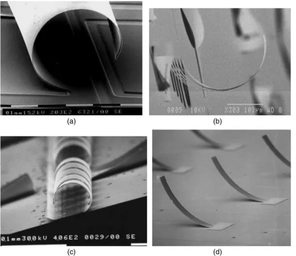
This review will describe the various approaches used in controlling the light transmission using microshutters based on curling electrodes and microelectromechanical system (MEMS) principles. It will compare performances and comment on challenges. Figure1presents an example of trapezoidal microblinds developed and fabricated at NRC.
1.1 Microelectromechanical System Microshutters MEMS devices are now everywhere, including in pressure sensors, accelerometers, inkjet printers, microphones, tele-communications switches, projectors, etc. They are also often identified as “micromachines” or “micro systems technology.” MEMSs usually have a mobile part that is actuated by either external forces (pressure, movement, etc.) or internal forces, such as electrostatic–magnetic forces. Their small sizes make them very sensitive to exter-nal or interexter-nal forces, as well as very robust mechanically. Their fabrication processes are derived from microelec-tronic manufacturing. Most MEMS devices are made or built on silicon (Si) substrates with some exception on glass substrates. Electrostatic MEMSs are particularly attractive because of their efficiency (high-energy density and large forces), design simplicity, fast response, and low power consumption.40
This review focuses on microshutters fabricated on glass substrates to control the light transmission. Other groups such as the one at NASA41 have worked on microshutter arrays based on Si substrates The devices described in this review are similar to cantilevers (basic MEMS structure). Nevertheless, microshutters have the top mobile electrode curling up based on stress gradient. The last layer(s) depos-ited get freestanding or mobile after etching away the
sacrificial or release layer. When applying a voltage (electric field) between the bottom and the top electrodes, the top electrodes roll down onto the surface, thus blocking the light transmission.
1.2 Materials
The choice of materials being deposited for the various layers is critical for the reliability of MEMS devices.42It also deter-mines their operating conditions as well as their manufactur-ing cost over large areas. The bottom electrode is usually a transparent conductive oxide (TCO), such as indium tin oxide (ITO), tin oxide (SnO2), zinc oxide (ZnO), or even silver (Ag)-based conductive layers. These layers will reduce the light transmission by a certain amount; some of them may also significantly reduce the transmission of near-infrared light critical for maximum solar heat gain in cold climates. The insulating or dielectric layer(s) are critical as well since a high electric field will exist between both electrodes. Most research groups have usedSiO2as an insu-lating layer (a common dielectric for microelectronics), whereas some others have usedSiNx,Al2O3, and polymers. The reliability of the microshutters depends strongly on the performances (for example, breakdown voltage and leakage current) of the dielectric layer(s).43–46 A sacrificial (or release) layer is then deposited on the dielectric. The top electrode is usually made of metal (Cr, Al, Au, sometimes combined with a dielectric layer). Once the sacrificial layer is etched away, the top electrode becomes freestanding and mobile.
The choice of materials is also critical for the general reli-ability of the device, for example, their stabilities in chemical environment (humidity, oxygen), temperature cycling, or UV exposure are keys for long-term reliability. In this context, hard, high melting point, inorganic materials are often pre-ferred over less stable materials. Some switchable glass tech-nologies that are sensitive to UV have added UV-blocking layers or stabilizers at the expense of reducing the UV (long wavelengths) benefits of daylight.
1.3 Fabrication Steps
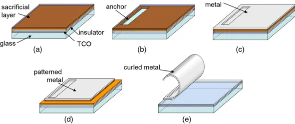
Most microshutters are based on standard microelectronic fabrication processes, such as e-beam evaporation, magnet-ron sputtering, optical lithography, and plasma etch and deposition. Figure2presents the main fabrication steps for the microshutters presented in this work.
The lithography (layer patterning) steps are particularly critical for defining the various planar geometries. More lithography steps result in an increased cost of manufactur-ing. These steps could be performed using conventional opti-cal lithography (contact or projection) or printing techniques or could be laser-based.
The gradient of stress in the top electrode determines the curling behavior. The control of the stresses is crucial in order to get reproducible and uniform results (radius of cur-vature, actuation voltage, etc.) Many groups17,26,31have used magnetron sputtering to deposit the top electrode to tune the intrinsic stresses. University of Tokyo27has used evapo-ration techniques, relying on material dependent stresses. Other groups22,27,32 have taken advantages of the different coefficients of thermal expansion (CTEs) of bilayers. Universities of Kassel24 and Stuttgart35 have used plasma-enhanced vapor deposition (PECVD) layers with stress
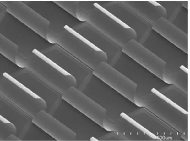
Fig. 1 Scanning electron microscopic (SEM) image of an array of trapezoidal microblinds (microshutters) fabricated at the NRC.
gradient. Controlling and characterizing the stress are the keys to reproducible and reliable devices.
The release of the mobile top electrode is performed by removing (etching) the sacrificial layer. This could be done by dry etching or wet etching, depending on the nature of the layers. The choice of the sacrificial layer is often made in such a way that it can be selectively removed without attack-ing the remainattack-ing layers in the device such as the dielectric layer and the top electrode. For example, NRC’s microshut-ters (microblinds) use a very thin sputtered amorphous Si layer as a sacrificial layer, which is etched away using fluo-rine-based plasmas or wet chemistries. This release step is delicate and can lead to fabrication issues such as improper curling up.29 Some groups28–31 have included special and
extra patterning steps (such as corrugation) to promote the proper release or curling behavior.
1.4 Design
Depending on the required performances, individual micro-shutter area may vary from a few square microns to a more macroscopic order (cm2). They can be individually con-nected together or grouped by areas. The patterning steps required for manufacturing the microshutters may be viewed as a weakness, compared to other switchable glasses technol-ogies, but it can also be considered a strength for applications that demand selectively actuated areas or even individually addressed microshutters using passive or active matrix thin film transistor (TFT) technologies. For this purpose, and for facilitating the dimming or improving the reliability of the devices, various groups have chosen to also pattern the bottom electrode.
Most research groups did not report any analytical or mathematical approaches to design their devices. However the U.S. Air Force29 used mathematical expressions devel-oped for cantilevers. Other groups performed modeling using simulations software such as Fiat (Ansys), NRC (Comsol), and INO (Intellisuite).
1.5 Actuation
Microshutters are based on MEMS devices, more specifi-cally on capacitive MEMSs. There are many publications43,44
describing how to reliably actuate capacitive MEMS devices. The most popular methodology to actuate electrostatically driven microshutters is by using bipolar square waves at frequency around 100 to 1000 Hz. It is also possible to actuate them using DC voltages. The operation voltage varies from 10 V to a few hundred volts depending on the dielectric used, its size, the release layer thickness, and the top electrode (stress and thickness). There is a lot of know-how behind the actuation especially when millions of micro-shutters are simultaneously actuated on the same device. 2 Various Versions of Microshutters
As mentioned in Sec.1, many versions of microshutters have been reported in the literature and on the web. This section will briefly describe each of the many versions reported in the published literature and compare them.
2.1 New Visual Media Group, United States
NVMG has developed electropolymeric shutters based on shrinkable polymer-laminated using rolls.22 They may be considered milli- or mini-shutters instead of microshutters because of their size of the order of millimeters and larger. They follow the work done by Charles G. Kalt some 30 years ago (resulting in more than 20 patents, for example, Ref.47). These devices are included in this review since their working principle (electrostatic forces unrolling a mobile electrode) is the same as the usual microshutters. Moreover, they are the only ones commercially available on large area. The stressed curling top electrode is based on shrinkable polymer (1- to5-μm thick). Once rolled up into multiple turn coils, their diameter is around 1 to 5 mm or greater. The dielectric is based on polymer (4- to10-μm thick). Their fabrication involves roll laminator and adhesives. The operation voltage usually ranges between 100 and 500 V DC.
Most of the details are available from their patents, but they also have a website23 where videos demonstrating the technology are available.
2.2 National Research Council Canada
NRC’s microshutters have been called microblinds.17
Fig. 2 Typical fabrication scheme for microshutters. (a) Glass substrate coated with TCO, insulator, and sacrificial layer; (b) patterning and etching of the sacrificial layer to define the anchor; (c) deposition of the top electrode; (d) patterning the geometry of the microshutters by etching the top electrode; and (e) releasing the microshutters by removing the sacrificial layer.
Details about microblinds are available through few conference proceeding paper,17patent, and web presence.18,48
Their video has been quite popular, and they have been cited in few reviews on switchable glass14,15and market reports.19–21 They successfully tried various TCOs. The desired stress gradient in the top electrode is obtained using magnetron sputtering (varying deposition conditions) [Fig.3(a)]. They optimized the dielectric to improve the reliability. The thin sacrificial layer (a:Si, 40-nm thick) and the thin top electrode allow the microblinds to be operated at relatively low volt-ages (around 20 V). Their fabrication scheme is relatively simple. Nevertheless, it leads to an impressive blockage in closed state (around 99.9%). The microblinds can be fabri-cated by regular microelectronic or flat panel display (FPD) technologies but also possibly using laser patterning for yielding a much lower fabrication cost.
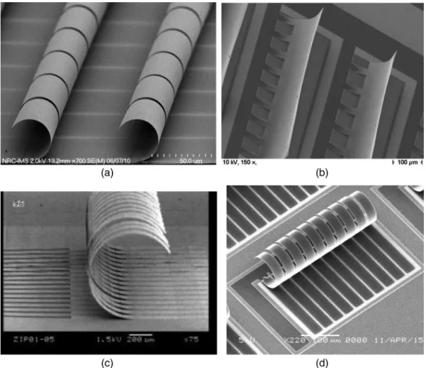
2.3 University of Kassel, Germany
University of Kassel has been developing optical MEMS micromirrors for daylight steering.24,25 They are a kind of microshutters with curling hinges and a flat micromirror [Fig.3(b)]. Their micromirrors are also actuated by electro-static voltages (40 to 100 V). Their sacrificial layer is usually based on photoresist, and their usual stress gradient is obtained using PECVD. Many papers and dissertation
theses in which they described the various fabrication schemes are available.
2.4 Institut National d’Optique, Canada
INO developed microshutters for spectrometry applications.26 They are not aimed for large areas but mainly to cover slits in front of spectrometers. Each individual microshutter has a length of 1 mm and a width of60 μm [Fig. 3(c)]. Contrary to most microshutters, they do not use TCO as a bottom electrode, but rather side electrodes made of Al layer. The dielectric isSiNx, the sacrificial layer is based on photoresist, and the top electrode is based on MoCr. The stress gradient is obtained by varying deposition conditions during the mag-netron sputter deposition.
2.5 University of Tokyo, Japan
The University of Tokyo developed microshutters using stress gradient based on evaporated metal on SiO2 at 180°C.27 The different CTEs create the stress gradient at room ature but may make them sensitive to the operating temper-ature. Each individual shutter is200-μm long, 30-μm wide, and0.3-μm thick [Fig.3(d)]. The sacrificial layer is photo-resist. The closing speed is around 3 ms and the operating voltage is 55 V.
Fig. 3 SEM images of microshutters developed at (a) NRC, (b) University of Kassel (reproduced from Ref. 25 with permission of Springer), (c) INO (reproduced from Ref. 26 with permission of SPIE), and (d) University of Tokyo (reproduced from Ref. 27 with permission of IEEE).
2.6 Samsung, Korea
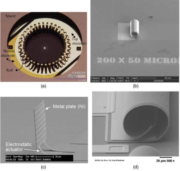
Samsung developed a 2-mm diameter iris shutter for camera using MEMS microshutters.28,49 The iris is formed out of 36 individual 1.4-mm-long triangular shutters [Fig. 4(a)]. On their first reported attempt, they used SiNx∕Al bilayer top electrode. Their second report pointed out a detrimental temperature sensitivity when usingSiNx∕Al; they switched to Mo/Mo for better results. Mo/Mo describes two layers of Mo with different intrinsic stresses and ideal insensitivity to temperature. Their operating voltage is 30 V. They used corrugation to improve the curling and dimples to reduce stiction.
2.7 United States Air Force
USAF Research Laboratory developed microshutters for adaptive coded aperture imaging and nonimaging applica-tions.29They used AlZnO as the TCO on fused silica, and the dielectric isSiNx. The sacrificial layer is0.5-μm photo-resist and the top electrode is made of Ti and Au [Fig.4(b)]. Their research compared models of the DC actuation to their fabricated devices. These shutters used corrugations
to improve the curling up but also revealed the difficulty of releasing depending on the geometry of the microshutters. 2.8 Korea Advanced Institute of Science and
Technology
KAIST developed cascaded microshutters for variable trans-mission in next-generation displays.30,31Their microshutters
are composed of ITO/SiO2/photoresist (sacrificial)/Ti-Au and require four patterning steps, including one to make cor-rugations [Fig.4(c)]. The gradient of stress in the top elec-trode is based on different intrinsic stresses of sputtered Ti and Au layers. They measured a pull-in voltage of 20 V and a closing speed of20 μs. Reliability testing of the first-level microshutters revealed some dielectric charging; never-theless, they estimated their lifetime to 500 billion cycles. 2.9 Microelectronic Center of North Carolina,
United States
MCNC and the University of Florida developed microshut-ters for protecting optical sensors.32Their microshutters are based on polyimide as the dielectric and Al as a sacrificial
Fig. 4 Images of microshutters developed at (a) Samsung (reproduced from Ref. 28 with permission of IEEE), (b) USAF (reproduced from Ref. 29 with permission of SPIE), (c) KAIST (reproduced from Ref. 31 with permission from SID), and (d) MCNC (reproduced from Ref. 32 with permission from SPIE).
layer [Fig.4(d)]. The top electrode is based on a sandwich of polyimide/Cr/Au/polyimide. The stress gradient is induced during the curing of the polyimide. They also experienced curling issues. Their operating voltage is around 100 to 300 V; the closing speed is measured as18 μs. They reported that low operating voltages yield longer lifetime, and 450 million cycles were tested.
2.10 Fiat, Italy
They developed microshutters for display and spectroscopy applications [Fig.5(a)].33,34They did not reveal much about the fabrication; nevertheless, their microshutters are rela-tively big (0.5 to 2 mm) and required around 80 V actuation voltage. Modeling results were obtained in collaboration with the Université de Bordeaux.
2.11 University of Stuttgart, Germany
Following a collaboration with NRC, University of Stuttgart decided to implement microshutters with their TFT expertise.35 Their microshutters are mainly aimed toward display application with low aperture ratio (15%) [Fig.5(b)]. They are fabricated on TFT-based active matrices with a wet-etched Si sacrificial layer (150 to 200 nm thick).
The top electrode is SiNx with gradient of stress obtained during PECVD, and a molybdenum-tantalum (MoTa) con-ductive layer (total thickness around 500 nm). The operating voltage is around 30 V, and they estimated a response time below50 μs.
3 Comparison of the Various Approaches
Table1presents the various versions of microshutters devel-oped as a function of year (first publication known to us), material choice (bottom electrode, dielectric, sacrificial, top electrode), sizes, and fabrication processes. The references shown usually correspond to the latest publications. The first dates correspond to the date of first publication (paper or patent), although we recognize that work started before pub-lications were made. Many of the research groups developed microshutters several years ago and stopped the R-D project for unknown reasons. Most of the groups used ITO for the bottom electrode. There is a diversity of materials (polymer, Si, and Al) used for the sacrificial layer. This choice is critical for the fabrication (ability to etch quickly, manufacturing cost) as well as for the operating voltage. The ability to coat a very thin sacrificial layer without pinholes reduces the actuation voltage and thus increases the microshutter life-time. Most of the microshutters have sizes around200 μm;
Fig. 5 SEM images of microshutters developed at (a) FIAT (reproduced from Ref. 34 with permission of Springer), (b) University of Stuttgart (reproduced from Ref. 35 with permission of SID), (c) Philipps (repro-duced from Ref. 36 with permission from The Royal Society of Chemistry), and (d) PARC (repro(repro-duced from Ref. 37 with permission of SPIE).
Table 1 Comparison of the variou s micr oshu tters depen ding on materials an d fabrica tion. Mater ials Fab rication R esearch gr oup Ref. Time Botto m elec trode Dielec tric Sacr ificial Top elec trode Size Process es, comm ents N VMG 22 2007 to presen t TCO Pol ymer (4 -to 10 -μ m thick) Shrin kable polyme r laye r (1 -to 5 -μ m thick ) with Al, NiCr, SS (1 00-to 500-A thick) Centi meter (r: 0.5 to 2 mm or greater ) Tem peratur e-induce d stress, elec tropolymeric, roll lam inat or NR C 17 2005 to presen t SnO 2 , ITO, Ag low-e SiO 2 , SiN x ,A l2 O3 Si and others, ar ound 40 nm Cr and others, 1000 A 50 to 30 0 μm (r: 10 to 100 μm) Opt ical or laser patter ning, magn etron sputte ring U niversity of Ka ssel 24 2003 to presen t ITO, ZnO or Ag low-e SiO 2 , polyme r Phot oresist, 0 .5 μm SiO 2 – SiN x – Al – Cr 150 × 400 μm PEC VD stress and Al thick ness, opti cal lith o or imp rintin g IN O 26 2008 to 2009 Al SiN x Pol yimid e MoC r 60 × 1000 μm( r∶ 370 μm) Str ess control led during sputte r dep U niversity of Toky o 27 2015 to 2016 ITO, 200 nm SiO 2 , 200 nm Phot oresist, 0.5 to 2 μm SiO 2 , 200 nm ∕Al, 100 nm 200 × 100 μm( r∶ 70 μm) Al evap orated at 180°C on SiO 2 Sa msung 49 2009 to 2011 ITO PEC VD SiO 2 0: 5 μm Pery lene SiN x – Al (3500/3 000 A), Mo/Mo Iris, 2-mm diame ter, 36 1.4-m m-long triangular shutte rs (r: 230 to 500 μm) Sim ilar CTE is mu ch better . Cor rugations and dim ples are patt erned. Air Force 29 2008 AlZn O SiN x Phot oresist, 0 .5 μm Ti –Au 200 × 50 Cor rugation, difficulty to ro ll them up depen ding on geome try KAIS T 31 2010 to 2016 ITO, 0 .2 μm SiO 2 , 0 .5 μm Phot oresist, 0 .2 μm Ti –Au 100 nm 200 × 160 μm Fou r pat terning steps, different intrin sic stress of sputte red Ti and Au MCN C 32 2000 to 2002 ITO Pol yimid e, 0 .5 μm Al Pol yimid e– Cr –Au – poly imide Vario us sizes 50 μmt o 1 mm (r: 50 to 100 μm) PI cured at 40 0°C Fia t 33 1999 to 2005 ITO 458 μm to 2.4 mm U niversity of Stu ttgart 35 2016 to presen t MoT a SiN x Si, 150 to 200 nm MoT a on stresse d SiN x (4 00 to 600 nm) 200 μm (r: 64 to 300 μm) Str uctural SiN x with stre ss gr adient, re lease by wet etchi ng the Si
those dimensions should make them reliable (MEMS) as well as practically invisible to the eye.
There are different strategies used to make the top elec-trode. This is a very crucial step: the gradient of stress in the top electrode needs to be well controlled and uniform over relatively large areas depending on the applications.
It seems that more reproducible and uniform stress gra-dients are expected with magnetron sputtered layers (given the fact that targets can be over 4-m long and that it is a low-temperature process) than with evaporated, PECVD, or thermally cured layers for large areas.
Moreover, as Kim and Hong (Samsung)49 pointed out,
with experimental results, that stress gradients in the same material is much more temperature-stable than in bilayers such asAl∕SiNx. The different CTEs may have detrimental effects on switchable glass, unless used on thermally acti-vated switchable glass.
Contrary to most switchable glass, microshutters require patterning steps to define the anchors and the microshutters. These steps are usually based on optical lithography and represent a major manufacturing cost. Most microshutters require two patterning steps, but many research groups reported a required extra one for corrugating the top elec-trode. This extra step makes it easier to release and curl up successfully the top electrode but increases the manufac-turing costs. Two groups have investigated other patterning approaches, such as imprinting (University of Kassel) and laser patterning (NRC). These approaches could lead to much lower manufacturing costs.
As for the reliability, many researchers have proven experimentally that the microshutters (at least on small areas) are very reliable, cycling them millions of time.24,30,32
Table 2 presents the various microshutters based on their actuation voltages, speeds, demonstrated sizes, visible transmissions, and applications. The required performances depend on the application; however, there are obvious general advantages in low operating voltage, high contrast, temperature stability (no CTE gradient in top electrode, high-melting-point materials), UV durability (inorganic), and low manufacturing cost (thin layers and simple patterning).
The operating voltage is a critical parameter for many applications and the electric field is critical for the reliability of the devices. They depend on the dielectric, the mechanical properties of the top mobile electrode, the radius of curva-ture, the thicknesses of dielectric, space, and top electrode. The operating speed is inversely proportional to the size and thickness of the microshutters.
Scaling-up. Most research reports on microshutters are for devices covering only small areas. Although a few groups have made devices on opaque wafers, most work is designed to control light transmission (switchable glass) on small areas, such as spectrometer slits and eyeglasses, or large areas, such as car sunroof, aircraft windows, or even building windows. The electrostatic principle of operation scales to large areas as demonstrated by NVMG.22,23 FPDs based on LCDs are functionally similar to switchable glass and integrate additional complex electronics. These devices are made on glass panels as large as 3.4 m and require many high
Table 2 Comparison of the various microshutters depending on performances.
Research group Ref. Actuation Speed
Demo size (active area)
Max/min transmission
contrast Applications comments
NVMG 22 100 to 500 V second 5000 cm2 High contrast Macro-curling shutters, commercialized, eight U.S. patents issued, impressive demos
NRC 17 15 to 25 V Around40 μs to close
20 cm2 60/0.1 to 600 High contrast, low voltage
University of Kassel 24 40 to 100 V 100 cm2 80/5 to 16 Mirror steering sunlight; lifetime>50 years, startup
INO 26 110 V 2 ms to close, 7 ms to open
<1 cm2 Low contrast Space instrumentation (slit for spectrometer), substrate: sapphire
University of Tokyo 27 55 V 3 ms 0.25 cm2 53/36 Implemented on TFT Samsung 49 30 V 1 to 2 ms Iris of
0.04 cm2 High contrast Shutter for camera
Air Force 29 Low contrast Adaptive coded aperture imaging
KAIST 31 20 V 20 μs to close Small Low contrast Active transparent display MCNC 32 100 to 300 V 18 μs 5 cm2 Low contrast Eyelid for protection Fiat 33 80 V 0.1 ms Low contrast Display
University of Stuttgart 35 25 to 45 V <50 μs (model) 2 cm2 Low contrast Display, implemented on TFT, low transmission
resolution patterning steps. Large area microshutter panels are less complex than LCD panels but can be fabricated with similar manufacturing processes lines. Most research groups already used glass as a substrate and fabrication processes already employed in large scale manufacturing.
The operation voltage does not depend on the size of the area covered by the microshutters (voltage driven). Nevertheless, the total current will not only depend on area but also mostly depend on the operation frequency. The NRC modeled the effect of size, electrodes’ resistivities, dielectric and operation frequency on actuation. They found that scaling-up is not limited by the voltage distribution if the right materials and geometries are used. Realistically, it makes sense to target small- and mid-sized applications, before addressing the building window market. As pointed out earlier, laser processing could allow the microshutters to become a very competitive switchable glass technology for large areas such as building windows.
4 Weaknesses and Challenges
Microshutters are very different from the current most common switchable glass technologies, such as EC. For example, microshutters are particularly fast switching, with-out unintentional tint, low power consumption, superior for solar use-control, and area-selective. Moreover, the microshutters with single material top electrode and without organic materials might be temperature-stable and UV-durable. One of the requirements for many applications, such as car sunroof and augmented reality, is the possibility to implement the switchable glass on curved glass substrates. EC did not succeed yet to reach that goal. Some micro-shutters based on high-melting-temperature materials (e.g., Ref.17), can be implemented on glass substrates to be bent. Nevertheless, microshutters still have weaknesses, such as visual disturbance, required enclosure/encapsulation, manu-facturability on large areas at low cost, reliability, and stress control. For example, the microshutters once curled up become tiny opaque lines that induce Fresnel diffraction, resulting in haze or visual disturbance. This diffraction is inherent to the technology, but it is also possible to reduce the resulting haze to an indiscernible level. There is a real market pull to develop such a switchable glass. The micro-shutters might not replace completely the competitive tech-nologies. However, for applications where speed, contrast, durability, and temperature stability are critical, they might be the best candidate.
5 Conclusion
Microshutters have very interesting performance levels, making them good candidates for switchable glasses or light modulators. Many research groups have investigated various approaches to fabricate microshutters. They proved that microshutters can be reliable on small scale, fast, low power, high contrast, and relatively easy to manufacture. There is a need to prove that they can also be scaled-up and cost-competitive.
Acknowledgments
We wish to thank Heping Ding, Kelly Laliberté, Richard Dudek, Mark Malloy from NRC, Rob Vandusen from Carleton University, and Patrick Schalberger from University of Stuttgart.
References
1. K. Butti and J. Perlin, A Golden Thread: 2500 Years of Solar Architecture, Cheshire Books, Palo Alto, California (1980). 2. A. K. Fahimipour et al.,“Daylight exposure modulates bacterial
com-munities associated with household dust,”Microbiome6(1), 175–187
(2018).
3. D. R. Roberts,“Preliminary assessment of the energy-saving potential of electrochromic windows in residential buildings,” Technical report NREL/TP-550-46916, National Renewable Energy Laboratory (2009). 4. A. H. Sadek and R. Mahrous,“Adaptive glazing technologies: balancing the benefits of outdoor views in healthcare environments,”Sol. Energy
174, 719–727 (2018).
5. S. Attia et al.,“Current trends and future challenges in the performance assessment of adaptive façade systems,”Energy Build.179, 165–182
(2018).
6. A. Piccolo et al.,“Energy performance of an electrochromic switchable glazing: experimental and computational assessments,”Energy Build.
165, 390–398 (2018).
7. A. Cannavale, U. Ayr, and F. Martellotta,“Innovative electrochromic devices: energy savings and visual comfort effects,”Energy Procedia
148, 900–907 (2018).
8. J.-M. Dussault, L. Gosselin, and T. Galstian,“Integration of smart windows into building design for reduction of yearly overall energy consumption and peak loads,”Sol. Energy86(11), 3405–3416 (2012).
9. E. Syrrakou, S. Papaefthimiou, and P. Yianoulis, “Eco-efficiency evaluation of a smart window prototype,”Sci. Total Environ.359(1–3),
267–282 (2006).
10. J. Al Dakheel and K. T. Aoul,“Building applications, opportunities and challenges of active shading systems: a state-of-the-art review,”
Energies10(10), 1672–1703 (2017).
11. Y. Wang, E. L. Runnerstrom, and D. J. Milliron,“Switchable materials for smart windows,”Annu. Rev. Chem. Biomol. Eng.7, 283–304 (2016).
12. R. Baetens, B. P. Jelle, and A. Gustavsen,“Properties, requirements and possibilities of smart windows for dynamic daylight and solar energy control in buildings: a state-of-the-art review,” Sol. Energy Mater. Sol. Cells94(2), 87–105 (2010).
13. M. Casini,“Active dynamic windows for buildings: a review,”Renew. Energy119, 923–934 (2018).
14. J. Marchwiński, “Architectural evaluation of switchable glazing tech-nologies as sun protection measure,”Energy Procedia57, 1677–1686
(2014).
15. Y. P. Singh and M. S. Gupta,“Future of intelligent windows,” Int. J. Res. Eng. Technol. 4(3), 17–26 (2016).
16. S. D. Rezaei, S. Shannigrahi, and S. Ramakrishna,“A review of conven-tional, advanced, and smart glazing technologies and materials for improving indoor environment,” Sol. Energy Mater. Sol. Cells159,
26–51 (2017).
17. B. Lamontagne et al.,“The next generation of switchable glass: the micro-blinds,” in Proc. Conf. Glass Perform. Days, Tampere, Finland (2009).
18. B. Lamontagne,“Smart automotive headlamp based on arrays of optical shutters,” 2012, https://www.slideshare.net/BorisLamontagne/smart-automotive-headlamp-based-on-arrays-of-optical-shutters(17 September 2019).
19. MarketsAndMarkets,“Smart glass market by technology (Suspended particle display, electrochromic, liquid crystal, photochromic, thermo-chromic), application (architecture, transportation, consumer electronics), and geography—Global Forecast to 2023 2017,” Report Se-2552, 2017,
https://www.marketsandmarkets.com/Market-Reports/smart-glass-market-907.html(17 September 2019).
20. Research and Markets,“The global market for smart glass and windows to 2030,” 2018, ID:4615164, https://www.researchandmarkets.com/ research/7p62fr/global_smart?w=5(17 September 2019).
21. BCC Research,“Global markets and technologies for smart glass,” 2018, Report AVM065D, https://www.bccresearch.com/report/ download/report/AVM065D(17 September 2019).
22. E. Schlam, J. Finch, and J. Koskulics,“Highly reflective electrostatic shutter display,” in Proc. Int. Disp. Workshops, Sendai, Japan (2017). 23. New Visual Media Group, https://newvisualmediagroup.com/index
.php/technology(17 September 2019).
24. H. Hillmer et al.,“Optical MEMS-based micromirror arrays for active light steering in smart windows,”Jpn. J. Appl. Phys.57(8S2), 08PA07
(2018).
25. Q. Li et al.,“Design of self-assembling micromirror arrays for light guiding applications,”Microsyst. Technol.16, 895–899 (2010).
26. S. Ilias et al.,“Programmable optical microshutter arrays for large aspect ratio microslits,”Proc. SPIE7099, 70992D (2008).
27. K. Mori et al.,“A MEMS electrostatic roll-up window shade array for house energy management system,” IEEE Photonics Technol. Lett.
28(5), 593–596 (2016).
28. C. Kim, K. Jung, and W. Kim,“A wafer-level micro mechanical global shutter for a micro camera,” in Proc. IEEE 22nd Int. Conf. Micro Electro Mech. Syst., pp. 156–159 (2009).
29. D. Langley, S. Rogers, and L. Starman,“Fabrication studies for scaling photonic MEMS micro-shutter designs,” Proc. SPIE 7096, 709601
(2008).
30. K.-H. Lee, J. Chang, and J.-B. Yoon,“High performance microshutter device with space-division modulation,” J. Micromech. Microeng.
20(7), 075030 (2010).
31. K.-S. Lim et al.,“Wide bandwidth reflective microshutter blind panel for transparent organic light-emitting diode display,” inSID 2016 Int. Symp., San Francisco, Vol. 47, no. 1, pp. 1389–1391 (2016). 32. S. Goodwin-Johansson et al., “Reduced voltage artificial eyelid for
protection of optical sensors,”Proc. SPIE4695, 451–458 (2002).
33. P. Roux et al.,“Fem modelling of an electro-optical micro-shutter,”
Sens. Actuators A: Phys.119(1), 1–7 (2005).
34. M. Pizzi et al.,“Electrostatically driven film light modulators for display applications,”Microsyst. Technol.10(1), 17–21 (2003).
35. P. Schalberger, S. A. A. Nusayer, and C. Raichle,“Parallel fabrication for integration of electronic and microelectromechanical systems,” in SID 2016 Int. Symp., San Francisco, Vol. 47, no. 1, pp. 731–734 (2016). 36. J. Toonder et al.,“Artificial cilia for active micro-fluidic mixing,”Lab
Chip8(4), 533–541 (2008).
37. M. A. Rosa et al., “A novel external electrode configuration for the electrostatic actuation of MEMS based devices,” J. Micromech. Microeng.14(4), 446–451 (2004).
38. P. Deb Shuvra and S. McNamara,“The strain capacitor: a novel energy storage device,”AIP Adv. 4, 127158 (2014).
39. C. C. B. Bufon et al.,“Self-assembled ultra-compact energy storage ele-ments based on hybrid nanomembranes,”Nano Lett. 10, 2506–2510 (2010).
40. Y. Zhang and Y.-P. Zhao,“Flexural contact in MEMS stiction,”Int. J. Solids Struct.49(17), 2203–2214 (2012).
41. D. E. Burns et al.,“2-D electrostatic actuation of microshutter arrays,”
J. Microelectromech. Syst.25(1), 101–107 (2016).
42. V. T. Srikar and S. M. Spearing,“Materials selection for microfabricated electrostatic actuators,”Sens. Actuators A102, 279–285 (2003).
43. W. M. van Spengen,“Capacitive RF MEMS switch dielectric charging and reliability: a critical review with recommendations,”J. Micromech. Microeng.22, 074001 (2012).
44. H. Camon and C. Ganibal,“Advantages of alternative actuating signal for MEMS actuators,” Sens. Actuators A: Phys. 136(1), 299–303
(2007).
45. R. Saha et al.,“Analysis of pull-in-voltage and figure-of-merit of capaci-tive MEMS switch,”Trans. Electr. Electron. Mater.17(3), 129–133
(2016).
46. Y. Huang et al.,“MEMS reliability review,”IEEE Trans. Device Mater. Reliab.12(2), 482–493 (2012).
47. C. G. Kalt,“Electro-static device with rolling electrode,” patent USPTO US 4094590A (1976).
48. B. Lamontagne, “Micro-blinds for smart glass,” 2011, https://www .youtube.com/watch?v=RqwL2egaqYY.
49. C.-H. Kim and S. Hong,“Study on the reliability of the mechanical shutter utilizing roll actuators,” inProc. IEEE 24th Int. Conf. Micro Electro Mech. Syst., Cancun, Mexico, pp. 501–504 (2011).
Boris Lamontagne received his PhD in engineering physics from École Polytechnique, Montréal, in 1992. Postdocs in Paris and Quebec city were followed by a researcher employment at the National Research Council (NRC) in 1995. His research interests are fabrication of photonic and MOEMS devices.
Norman R. Fong is a research associate at the NRC, Ottawa, Ontario, Canada. He received his PhD in electrical engineering from Carleton University (2015) with research focus on micro- and nano-fabrication of integrated plasmonics and microelectromechanical system (MEMS) sensors.
In-Hyouk Song received his PhD in electrical engineering from Louisiana State University, Baton Rouge, Louisiana, in 2005. He served as a research associate at Ecole Polytechnique de Montreal, Montreal, and NRC, Ottawa, Canada. Since 2010, he has been at the Department of Engineering Technology, Texas State University, Texas, where he is currently an associate professor. His research efforts have focused on developing the physical and biosensing device combining MEMS techniques.
Penghui Ma received his PhD from University of Western Ontario in 1997. He is a senior research officer at NRC, Canada. His main research interests are in thin-film depositions, multilayer optical coat-ings, and their applications.
Pedro Barrios received his BSc degree in electronic engineering from the IUPFAN, Venezuela, in 1989, and his MS degree and PhD in electrical engineering from the University of Pittsburgh in 1993 and 1997, respectively. He worked as a postdoc at the NanoFAB Center of Texas A&M University from 1998 to 1999 and at the EE Department of the University of Notre Dame from 1999 to 2000. Currently, he pursues research in fabrication of optoelectronic devices on III–V semiconductors at the NRC of Canada in Ottawa.
Daniel Poitras received his PhD in physics engineering from Ecole Polytechnique Montreal with a thesis on plasma-deposited optical films and coatings in 2000. Currently, he is working as a senior researcher at the NRC of Canada. His main fields of interest are the application, design, fabrication, and characterization of optical coat-ings, with a recent focus on waveguide facet optical coatings.