A Column-Row-Parallel ASIC Architecture for 3D
Wearable / Portable Medical Ultrasonic Imaging
by
Kailiang Chen
B.E., Tsinghua University (2007)
S.M., Massachusetts Institute of Technology (2009)
Submitted to the Department of Electrical Engineering and Computer
Science
in partial fulfillment of the requirements for the degree of
Doctor of Philosophy
at the
MASSACHUSETTS INSTITUTE OF TECHNOLOGY
February 2014
c
Massachusetts Institute of Technology 2014. All rights reserved.
Author . . . .
Department of Electrical Engineering and Computer Science
January 31, 2014
Certified by . . . .
Charles G. Sodini
LeBel Professor of Electrical Engineering
Thesis Supervisor
Certified by . . . .
Anantha P. Chandrakasan
Joseph F. and Nancy P. Keithley Professor of Electrical Engineering
Thesis Supervisor
Accepted by . . . .
Leslie A. Kolodziejski
Chair, Department Committee on Graduate Students
A Column-Row-Parallel ASIC Architecture for 3D Wearable
/ Portable Medical Ultrasonic Imaging
by
Kailiang Chen
Submitted to the Department of Electrical Engineering and Computer Science on January 31, 2014, in partial fulfillment of the
requirements for the degree of Doctor of Philosophy
Abstract
This work presents a scalable Column-Row-Parallel ASIC architecture for 3D wear-able / portwear-able medical ultrasound. It leverages programmwear-able electronic addressing to achieve linear scaling for both hardware interconnection and software data acqui-sition. A 16x16 transceiver ASIC is fabricated and flip-chip bonded to a 16x16 ca-pacitive micromachined ultrasonic transducer (CMUT) to demonstrate the compact, low-power front-end assembly. A 3D plane-wave coherent compounding algorithm is designed for fast volume rate (62.5 volume/s), high quality 3D ultrasonic imaging. An interleaved checker board pattern with I&Q excitations is also proposed for ul-trasonic harmonic imaging, reducing transmitted second harmonic distortion by over 20dB, applicable to nonlinear transducers and circuits with arbitrary pulse shapes.
Each transceiver circuit is element-matched to its CMUT element. The high voltage transmitter employs a 3-level pulse-shaping technique with charge recycling to enhance the power efficiency, requiring minimum off-chip components. Compared to traditional 2-level pulsers, 50% more acoustic power delivery is obtained with the same total power dissipation. The receiver is implemented with a transimpedance amplifier topology and achieves a lowest noise efficiency factor in the literature (2.1 compared to a previously reported lowest of 3.6, in unit of mP a ·qmW/Hz). A source follower stage is specially designed to combine the analog outputs of receivers in parallel, improving output SNR as parallelization increases and offering flexibility for imaging algorithm design. Lastly, fault-tolerance is incorporated into the transceiver to deal with faulty elements within the 2D MEMS transducer array, increasing yield for the system assembly.
Thesis Supervisor: Charles G. Sodini
Title: LeBel Professor of Electrical Engineering Thesis Supervisor: Anantha P. Chandrakasan
Acknowledgments
Finishing my Ph.D. is not possible without the enduring love from my parents and wife. I would like to thank them for all their support. Recently we have been through difficult moments together, but I look forward to the good days to come.
I feel extremely fortunate to work under the joint supervision of Prof. Charlie Sodini and Prof. Anantha Chandrakasan. I am grateful to Charlie, who is a great teacher for me inside and outside of school. I learned from him to always try to seek for insight and intuition behind a problem. I also learned from him to be down-to-earth, yet persistent, both in research and in life. I enjoyed our conversations, softball games played together for MTL, Redsox games, and of course, the Hong Kong trip. All of them are unforgettable.
I would like to express my gratitude to Anantha. Even as the Department Head with an incredibly busy schedule, I was able to receive ample guidance from him. He is always resourceful and creative, which sets me a standard for a good researcher.
I would like to thank Prof. Greg Wornell for being in my thesis committee and providing insights about imaging system trade-offs; Prof. Harry Lee for providing many clever circuit design ideas; Dr. Kai Thomenius for teaching me a lot of ul-trasonics know-how; Dr. Brian Brandt for continued support for my test setup and career development; Prof. Thomas Heldt, Tom O’Dwyer, Dr. Dennis Buss, Dr. Peter Holloway, and Mr. Haiyang Zhu for many useful technical discussions. I am thankful for all their help to my project.
I am grateful to people who helped me with the hardware system assembly, which is the key to the successful project demonstration. The ASIC fabrication is gener-ously made possible through the TSMC University Shuttle Program. The CMUT samples are obtained from Prof. Butrus (Pierre) Khuri-Yakub’s research group at Stanford University; students Byung Chul Lee, Anshuman Bhuyan, and Jung Woo Choe offered me many handy tips to work with the device. The CMUT-PCB-ASIC flip-chip bonding assembly was done with the help of Dr. Helen Kim and MIT Lin-coln Laboratory. The acrylic oil tank and the 3D translation stage were designed and
built with the assistance of MIT Central Machine Shop.
It has been a pleasant journey because of my colleagues in the Sodini/Lee lab and the Anantha group. In particular, I would like to thank Bonnie Lam, Sabino Pietrangelo, Joohyun Seo, and Katherine Smyth for a lot of intriguing discussions about ultrasonics. Also, I would like to thank Sunghyuk Lee, SungWon Chung, Wei Li, and Marcus Yip for the tremendous help during my tape-outs. Daniel Piedra, Allen Hsu, Bin Lu, and Jerome Lin taught me how to operate a probe station to take accurate measurements on a bare silicon die. Moreover, I would like to thank David He, Amanda Gaudreau, Philip Godoy, Jack Chu, Grant Anderson, Doyeon Yoon, Xi Yang, Eric Winokur, Maggie Delano, Daniel Kumar, Bruno Do Valle, and many more for being great labmates with whom I could hang out and have fun. Last but not least, Coleen Milley and Margaret Flaherty have been very supportive in logistics, who always make sure everything in lab runs smoothly.
This project is funded by the C2S2 Focus Center, one of six research centers funded under the Focus Center Research Program (FCRP), a Semiconductor Research Corporation entity; Texas Instruments; and the MIT Center for Integrated Circuits and Systems (CICS).
Contents
1 Introduction 23
1.1 Motivation . . . 23
1.2 The Challenge for Implementing a 3D Wearable / Portable Ultrasonic Imaging Device . . . 24
1.3 Contribution . . . 25
1.4 Thesis Organization . . . 26
2 Background Information 29 2.1 Ultrasonic Imaging Modes . . . 29
2.2 The Beam-formation Principle . . . 32
2.3 Ultrasonic Transducers . . . 34
2.4 Field II Simulation Program . . . 36
3 The Column-Row-Parallel Architecture for 3D Ultrasonic Imaging 39 3.1 The Prior Art of Architectures for 3D Ultrasonic Imaging . . . 39
3.2 The Motivation of the Column-Row-Parallel ASIC Architecture . . . 42
3.3 The Column-Row-Parallel ASIC Architecture . . . 44
3.4 The Functionality of the Column-Row-Parallel Architecture . . . 49
3.5 Summary . . . 54
4 3D Ultrasonic Imaging System Experiments 55 4.1 The Hardware System Assembly . . . 55
4.1.2 The PCB-ASIC Connection . . . 60
4.1.3 The Flip-Chip Bonding Assembly Process . . . 62
4.1.4 Mounting onto the Oil Tank . . . 66
4.2 Plane-wave Coherent Compounding for Fast Volume Rate 3D Ultra-sonic Imaging . . . 68
4.2.1 PWCC for 2D Imaging . . . 69
4.2.2 Extending PWCC to 3D Imaging on the Column-Row-Parallel Architecture . . . 71
4.2.3 PWCC3D Results: Simulations and Measurements . . . 77
4.2.4 Discussion . . . 85
4.3 Interleaved Checker Board Tx Apertures with I&Q Excitations for HD2 Reduction in Ultrasonic Harmonic Imaging . . . 88
4.3.1 THI Principle and Previous Methods . . . 89
4.3.2 Tx HD2 Suppression on the Column-Row-Parallel Architecture 91 4.3.3 Experimental Results . . . 93
4.4 Annular Ring Apertures for Forward-looking Imaging Applications . . 96
4.4.1 Annular Ring Apertures on Column-Row-Parallel Architecture 96 4.4.2 Annular Ring Imaging Results . . . 99
4.5 Summary . . . 101
5 Design of the 16x16 Ultrasonic Transceiver Array ASIC with Column-Row-Parallel Architecture 103 5.1 High-Level Description of the Ultrasonic Imaging Transceiver Circuits and the Architecture Logic Implementation . . . 103
5.2 Tx Circuit Design . . . 107
5.2.1 Multi-Level Pulsing for Efficient CMUT Driver . . . 108
5.2.2 3-Level Pulser Circuit Design . . . 111
5.2.3 Tx Path Design for 2D Ultrasonic Transducer Arrays . . . 114
5.3 Rx Circuit Design . . . 116
5.3.2 LNA Transistor-Level Implementation . . . 120
5.3.3 Rx Path Design for 2D Ultrasonic Transducer Arrays . . . 122
5.4 Biasing . . . 129
5.5 The Fault-Tolerant ASIC Design for Faulty MEMS Devices . . . 131
6 ASIC Characterization 137 6.1 Tx Ultrasonic Power and Efficiency Measurement . . . 137
6.1.1 Measuring Acoustic Output Power . . . 138
6.1.2 Measuring Tx Efficiency . . . 141
6.2 LNA Characterization . . . 144
6.3 The Tx Beam-Steering Experiment . . . 149
6.4 The Pulse-Echo Experiment . . . 151
7 Conclusion 155 7.1 Summary of Contributions . . . 155
List of Figures
2-1 The typical signals and the operation for B-mode ultrasound. . . 30 2-2 Simplified block diagram of a ultrasound BF system, figure courtesy
of [27]. . . 32 2-3 A typical Field II flow diagram for ultrasonic system behavioral
simu-lation. . . 37
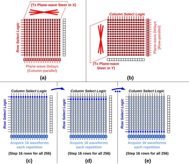
3-1 Column-parallel architecture implementations in the literature: (a) a 1D transducer array mechanically translated to scan the 3D space, ele-vation beam-formation is done by a synthetic virtual source technique, figure courtesy of [3]; (b) a 2D array operated to receive row-by-row, elevation beam-formation is done by sub-array delay-and-sum across the column using analog delay lines, figure courtesy of [55]. . . 41 3-2 The column-row addressing scheme implemented on a 256x256 2D
transducer array: (a) row-by-row transmit addressing; (b) column-by-column receive addressing; (c) the “Maltese cross” beam-pattern. Figure courtesy of [38]. . . 43 3-3 A column-row addressing architecture implemented at the circuit-level,
with column and row interconnections that reduce the system channel count and provide maximum flexibility for algorithms. . . 44 3-4 Column-Row-Parallel architecture block diagram, the CMUT and ASIC
3-5 (a) The block-level implementation of one transceiver channel and (b) the per-element logic implementation. Column and row select logic is implemented with shift registers that can be reprogrammed in “N ” time (implementation detail will be shown in Figure 5-2). . . 47 3-6 (a) Tx input port multiplexing, implemented with digital logic; (b) Rx
output port multiplexing, implemented with analog pass-gates. . . 49 3-7 The architecture configured in a column-parallel mode for the Tx
aper-ture. The configuration is broken down and illustrated in steps (a) through (d) to help understanding. Two rows are activated as the Tx aperture and beam-formation along azimuth (X) direction is achieved. 51 3-8 The architecture configured in a row-parallel mode for the Rx aperture.
Five columns are activated as the Rx aperture and beam-formation along elevation (Y) direction is achieved. . . 52 3-9 More use examples of the proposed architecture: (a) a diagonal Rx
aperture; (b) a checker board Tx aperture for ultrasonic harmonic imaging; (c) & (d) annular ring Tx and Rx apertures for forward-looking ultrasonic imaging applications. . . 53
4-1 System integration diagram showing the flip-chip bonding connection between CMUT and ASIC through a PCB interposer. The figure also shows the mechanical setup for imaging experiments, including an oil tank and a 3D translation stage. . . 56 4-2 The picture of the hardware system setup. . . 57 4-3 The block diagram of the hardware system setup. . . 57 4-4 The 16x16 CMUT die drawings: (a) the footprint of the CMUT; (b)
the CMUT flip-chip bonding pad metal structure drawing, courtesy of [40]. . . 58
4-5 The two different PCB designs made to fit CMUT footprints: (a) the PCB version A’s footprint for CMUT with a gap distance of 250µm; (b) the PCB version B’s footprint for CMUT with a gap distance of 373.75µm, only 1x16 pads are made on the PCB side due to space limitations. . . 59 4-6 The drawing of a PCB pad defined with a solder mask, and bumped
with a solder ball. The PCB pad is used to do flip-chip bonding to the CMUT die. . . 60 4-7 The ASIC die drawings: (a) the footprint of the ASIC, containing the
center 18x16 pads to be element-matched and connected to CMUT through the PCB interposer, and the surrounding I/O pads; (b) the PCB interposer layout design that allows the ASIC I/O pads to be routed out to the PCB edges. . . 61 4-8 The ASIC flip-chip bonding pad metal structure drawings: (a) the
hor-izontal view of a flip-chip bonding pad in ASIC; (b) the cross-sectional view of the ASIC flip-chip bonding pad. . . 62 4-9 The CMUT-PCB-ASIC two-step flip-chip bonding process: (a) first
step, the bonding between PCB and ASIC; (b) second step, the bond-ing between PCB and CMUT, with ASIC already bonded to PCB. . . 63 4-10 The CMUT-ASIC connection result pictures: (a) the bonded
PCB-ASIC assembly shows good connectivity; (b) the solder bumps at the PCB’s CMUT side is reflowed after PCB-ASIC bonding, any deforma-tion would be restored. . . 64 4-11 The PCB-CMUT bonding connection is verified by pulling off the test
CMUT die from the PCB after bonding and reflow. (a) & (b) show the CMUT connection posts remain on the PCB after the pull, indicating good connectivity. . . 64 4-12 The finished CMUT-PCB-ASIC assembly: (a) cross-sectional view of
the sandwich stack; (b) CMUT side assembly picture; (c) ASIC side assembly picture. . . 65
4-13 The acrylic tank drawings: (a) the tank dimension drawing; (b) the mounting between the oil tank and the CMUT-PCB-ASIC assembly. 66 4-14 The illustration of how PWCC works for 2D ultrasonic imaging,
cour-tesy of [68]. . . 69 4-15 The principle of coherent compounding used in PWCC, courtesy of [68]:
(a) the imaging space; (b) the beam-formation delay calculation when the transmitted plane-wave is normal to the transducer surface (α = 0o); (c) the beam-formation delay calculation when the transmitted plane-wave is steered to an angle of α. . . 70 4-16 The signal processing flow for PWCC3D on the Column-Row-Parallel
architecture. . . 73 4-17 The PWCC3D implementation on the Column-Row-Parallel
architec-ture: (a) Tx beam-steering along azimuth (X) direction using column-parallel mode; (b) Tx beam-steering along elevation (Y) direction using row-parallel mode; (c)-(e) Rx signal acquisition, sweeping through 16 rows for each transmit angle. . . 76 4-18 The sequence of operation to implement PWCC3D on the
Column-Row-Parallel architecture. . . 77 4-19 The setup of the wire phantom imaging experiment using PWCC3D
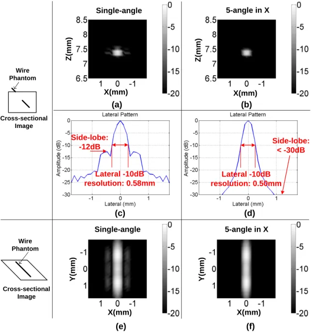
algorithm: (a) a single plane-wave is transmitted to image the wire phantom; (b) five different Tx angles are used along the azimuth di-rection for PWCC3D. . . 78 4-20 Simulation results of a wire phantom: (a) vertical cross-sectional
im-age produced from single angle plane-wave insonification; (b) verti-cal cross-sectional image produced from 5-angle coherent compounded wave insonification; (c) lateral resolution plot from single plane-wave; (d) lateral resolution plot from 5-angle plane-waves; (e) horizon-tal sectional image from single plane-wave; (f) horizonhorizon-tal cross-sectional image from 5-angle plane-waves. . . 80
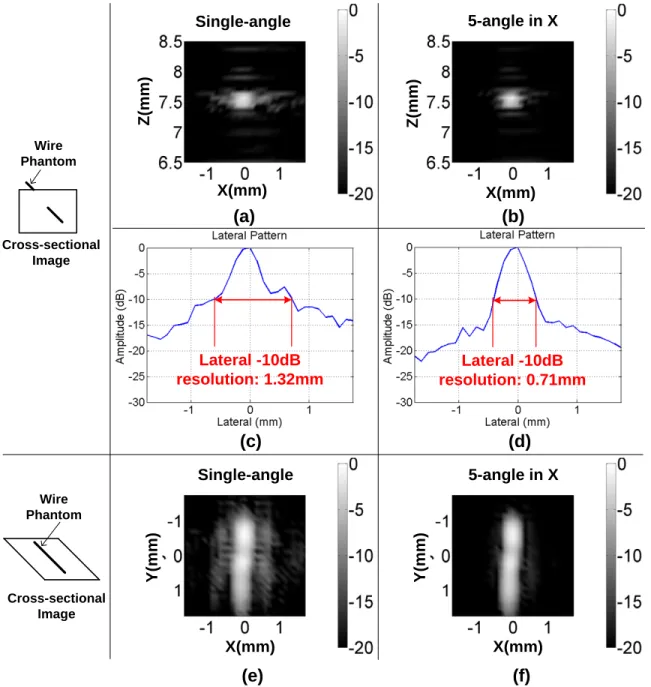
4-21 Measurement results of a wire phantom: (a) vertical cross-sectional image produced from single angle plane-wave insonification; (b) verti-cal cross-sectional image produced from 5-angle coherent compounded wave insonification; (c) lateral resolution plot from single plane-wave; (d) lateral resolution plot from 5-angle plane-waves; (e) horizon-tal sectional image from single plane-wave; (f) horizonhorizon-tal cross-sectional image from 5-angle plane-waves. . . 81 4-22 The setup of the ring phantom imaging experiment using PWCC3D
algorithm: (a) a single plane-wave is transmitted to image the phan-tom; (b) five different Tx angles are used along the azimuth direction and another five Tx angles along the elevation direction to image the phantom with PWCC3D. . . 82 4-23 Measured horizontal cross-sectional images of a ring phantom: (a)
single-angle Tx plane-wave; (b) 5-angle Tx plane-wave compounding along azimuth direction; (c) 5-angle Tx plane-wave compounding along elevation direction; (d) compounding across all angle azimuth and 5-angle elevation directions. . . 83 4-24 Measured vertical cross-sectional images of a ring phantom: (a)
single-angle Tx plane-wave; (b) compounding across all 5-single-angle azimuth and 5-angle elevation directions; (c) lateral resolution plot of ring image from single-angle Tx plane-wave; (d) lateral resolution plot of ring image from 5-angle X and 5-angle Y plane-waves. . . 84 4-25 Simulated XZ cross-sectional images showing the three cysts in one
slice image: (a) image generated from single-angle plane-wave; (b) image generated from 5 azimuth-angle and 5 elevation-angle plane-waves compounded; (c) the cross-sectional image location in 3D space. 85 4-26 Simulated YZ cross-sectional images showing the cyst at (−3, 0, 25)mm:
(a) image generated from single-angle plane-wave; (b) image generated from 5 azimuth-angle and 5 elevation-angle plane-waves compounded; (c) the cross-sectional image location in 3D space. . . 86
4-27 Simulated YZ cross-sectional images showing the cyst at (0, 0, 35)mm: (a) image generated from single-angle plane-wave; (b) image generated from 5 azimuth-angle and 5 elevation-angle plane-waves compounded; (c) the cross-sectional image location in 3D space. . . 86
4-28 Simulated YZ cross-sectional images showing the cyst at (3, 0, 45)mm: (a) image generated from single-angle plane-wave; (b) image generated from 5 azimuth-angle and 5 elevation-angle plane-waves compounded; (c) the cross-sectional image location in 3D space. . . 87
4-29 Implementation of checker board Tx aperture on the proposed archi-tecture. . . 91
4-30 Simulation comparison between the conventional and I&Q methods: (a) fundamental component spatial intensity for conventional; (b) fun-damental component spatial intensity for I&Q; (c) HD2 spatial inten-sity for conventional; (d) HD2 spatial inteninten-sity for I&Q. . . 94
4-31 Annular ring mode imaging implemented in Column-Row-Parallel ar-chitecture: (a) Tx and Rx aperture setup; (b) Tx aperture imple-mented in the proposed architecture, all active elements are driven in-phase; (c) Rx aperture with the biggest ring shape, all active el-ements’ analog outputs are combined; (d) Rx aperture with the 2nd ring shape; (e) Rx aperture with the 3rd ring shape; (f) Rx aperture with the smallest ring shape. . . 97
4-32 Annular ring mode dynamic beam-formation scheme. . . 98
4-33 Annular ring configuration example, off-center: (a) Tx and Rx aperture setup; (b) Tx aperture implemented in the proposed architecture; (c) Rx aperture with the biggest ring shape; (d) Rx aperture with the 2nd ring shape; (e) Rx aperture with the 3rd ring shape; (f) Rx aperture with the smallest ring shape. . . 100
4-34 Cross-section slices of the wire phantom 3D images from simulation and measurement: (a) simulated XZ slice; (b) measured XZ slice; (c) simulated YZ slice; (d) measured YZ slice; (e) simulated XY slice; (f) measured XY slice. . . 102
5-1 A re-plot of Figure 3-5 in Section 3.3. (a) The block-level implementa-tion of one transceiver channel and (b) the per-element logic implemen-tation. Column and row select logic is implemented with shift registers that can be reprogrammed in “N ” time (implementation detail will be shown in Figure 5-2). . . 105 5-2 Circuit implementation for the logic control: (a) multiplexing for
per-element enable bits; (b) Tx row / column selection logic; (c) Rx row / column selection logic. . . 106 5-3 (a) The transmitter load model of a CMUT element used in this work.
(b) An exemplary 2-level square wave pulse applied onto CMUT. (c) An exemplary 3-level pulse applied onto CMUT. . . 109 5-4 Circuit schematic of the four-channel 3-level pulsers with the
middle-voltage generation (all transistors are high middle-voltage devices). . . 111 5-5 The digital control circuits for the pulser: (a) the signal flow and block
diagrams; (b) the non-overlapping signal generator; (c) the level shifter implementation; (d) the control signal timing diagram. . . 113 5-6 Tx design for the 2D array: (a) 2D pulser schematic; (b) MUX
imple-mentation. . . 115 5-7 Small signal model and noise sources of the CMUT element and the
LNA. . . 117 5-8 Transfer functions when the LNA optimality condition is reached. . . 118 5-9 Transfer function examples when the LNA optimality condition of fi ≈
fp is not reached: (a) fi < fp, (b) fp < fi. . . 118
5-11 The LNA schematic, implemented in the TIA topology. All transistors are low voltage devices except the HV Rx Switch M10. . . 121 5-12 Design optimization for input stage transistors: (a) transistors are sized
at the boundary of strong and weak inversion; (b) transistor width is optimized for the lowest noise figure. . . 122 5-13 The signal and noise combining with two Rx channels in parallel: (a)
two channels on the same line, shown in Thevenin’s equivalent circuit at LNA outputs; (b) two channels on the same line, shown in Norton’s equivalent circuit at LNA outputs (c) two channels combined, showing the resultant signal and noise amplitudes. . . 124 5-14 The LNA schematic, implemented in the TIA topology. All transistors
are low voltage devices except the HV Rx Switch M10. “vip” node is also buffered with a source follower to output (not shown). . . 127 5-15 Parallelism with even more Rx channels by utilizing intermediate line
buffers to preserve the circuit performance. . . 129 5-16 The biasing circuit for the 2D array. . . 130 5-17 The technique used for detecting and isolating the short CMUT
el-ements: (a) front-end transistors in each channel and their control voltages; (b) the effective circuit connection of all 256 channels with CMUT elements. . . 133 5-18 Two successful 16x16 CMUT-ASIC assemblies with short CMUT
ele-ments (marked in red) isolated by the ASIC. The rest of the eleele-ments are functional and their sensitivity performance is expressed by the brightness of the elements, which will be described in detail in Section 6.4. . . 134
6-1 The photo of the lab setup for measuring the acoustic output power and the Tx efficiency. . . 139 6-2 Acoustic output power and Tx efficiency measurement setup. . . 140
6-3 Normalized RMS pressure along the transducer axial axis, measure-ment vs. simulation. The measuremeasure-ment deviates from the simulation in the near field because the hydrophone tip is too close to the trans-ducer surface, distorting the pressure field. . . 140 6-4 (a) Tx efficiency measurement setup and pulse shape definition. (b)
Measured time-domain waveform of the optimal 3-level 3.3MHz pulses, ∆=20ns, ∆/T=0.067 . . . 142 6-5 Tx efficiency measurement results using different 3-level pulse shapes
by varying the ∆/T ratio and at different frequencies. . . 143 6-6 The die photo of the four-channel ultrasonic imaging transceiver test
chip. . . 148 6-7 The die photo of the 256-channel 16x16 2D ultrasonic imaging transceiver
test chip. . . 149 6-8 (a) Measured ultrasonic lateral beam profile, steered to the center
(broadside). (b) Measured beam profile, with 30ns delay between chan-nels. . . 150 6-9 The setup of the pulse-echo experiment for characterizing the complete
ultrasound channel. . . 151 6-10 The key waveforms from the pulse-echo experiment, showing the
ul-trasound channel characteristics. (a) The transmitted pulse waveform. (b) The received echo waveform. (c) The spectrum of the received echo waveform. . . 152 6-11 A re-plot of Figure 5-18 in Section 5.5. Two successful 16x16
CMUT-ASIC assemblies with short CMUT elements (marked in red) isolated by the ASIC. The rest of the elements are functional and their sensi-tivity performance is expressed by the brightness of the elements. . . 153
7-2 CMUT-ASIC assembly alternatives to eliminate the interposer PCB: (a) TSV technology for interconnecting ASIC I/Os to the main test-ing PCB; (b) Applytest-ing flip-chip bondtest-ing technology for CMUT-ASIC interconnection and wire-bonding for ASIC I/Os. . . 159
List of Tables
4.1 Simulated HD2 improvement of the I&Q method. . . 95
4.2 Measured HD2 improvement of the I&Q method. . . 95
5.1 SNR improvement from Rx channel parallelism, theory prediction and measurement. . . 127
6.1 Measured Power and Efficiency Comparison at 3.3MHz for the 1D ASIC and CMUT (40pF capacitance per element) . . . 143
6.2 Measured Optimal 3-level Pulser Performance Summary for the 1D ASIC and CMUT (40pF capacitance per element) . . . 144
6.3 Measured Optimal 3-level Pulser Performance Summary for the 2D ASIC and CMUT (2pF capacitance per element) . . . 144
6.4 CMUT Pulser Performance Comparison . . . 145
6.5 Measured LNA Performance Summary for the 1D ASIC [5] . . . 145
6.6 Measured LNA Performance Summary for the 2D ASIC . . . 146
Chapter 1
Introduction
1.1
Motivation
Ultrasonic imaging is an important modality for medical diagnosis. Compared to other imaging modalities, ultrasound is relatively low cost, harmless to human health, and has decent resolution. Modern ultrasonic imaging systems are becoming increas-ingly complex and powerful, yet compact, benefiting from Moore’s law [1]. Laptop-size ultrasound systems have gained comparable performance to the traditional cart-size machines; hand-held devices, such as the GE Vscan [2], indicates the trend toward highly integrated ultrasonic imaging solutions to enable portable or even wearable ultrasound applications in hospital and at home.
Traditional 2D medical ultrasonic imaging systems have been in wide use for decades. A 2D imaging system uses a 1D ultrasonic transducer probe and gener-ates rectangular or sector-shape 2D cross-sectional images of human tissue or organs. These systems exist predominantly in hospital settings where professional sonogra-phers are available to operate the system. They would carefully angle and position the probe against the human body, so as to produce satisfactory 2D medical images for diagnosis. This process is manual and requires extensive training for the operators, adding complexity and extra cost to the diagnostic procedure.
On the other hand, 3D medical ultrasonic imaging systems provide a full view of human tissue or organs in space, rather than cross-sectional views in 2D imaging
systems. The 3D volumetric image data represent a more comprehensive set of data which could be more easily interpreted to help locate target of medical interest. As a result, the manual search of the “best” 2D slice image performed by the sonographers holding a 1D probe is possible to be substituted with an automated search algorithm in a 3D imaging system. Furthermore, by leveraging advanced microelectronics tech-nology, a compact and low-power ultrasonic hardware system can be built to enable wearable / portable self-monitoring ultrasonic imaging devices at home. Therefore, one could imagine an automated imaging system that continuously tracks human tis-sue or organs of interest and produces long-term medical information with minimum reliance on experienced sonographers.
1.2
The Challenge for Implementing a 3D
Wear-able / PortWear-able Ultrasonic Imaging Device
A typical 1D array for a 2D imaging system has an element count of as high as one thousand. The interconnection from the transducer elements to the interfacing electronics are co-axial cables. When it comes to 3D imaging systems, 1D ultrasonic transducer arrays had been used historically to acquire the 3D volumetric data, by being mechanically translated [3] or rotated [4] to cover the whole 3D space. A slice of 2D image is formed at each physical position of the 1D array. Multiple 2D slice images are stitched together to form the 3D volumetric image. These mechanical approaches have many disadvantages. For example, the image resolution tends to be poor due to the relatively large incremental step size of the mechanical movement; the image frame rate or volume rate could be limited by the mechanical movement speed; the system integration tends to be bulky and system power consumption is high because a mechanical motor is needed.
More recently, 2D ultrasonic transducer arrays made from a micromachining pro-cess have become more available and proven to be more suitable for 3D ultrasonic imaging. As a result, the mechanical movement is replaced by electrical addressing;
the coarse motor stepping is replaced by the much finer element-to-element spacing; the image frame rate or volume rate is no longer limited by the speed of mechanical movement; and system size and power are reduced to allow long-term wearable / portable hardware solutions.
However, an electronic system working with a 2D array is much harder to be built. Most notably, the interconnection between a 2D transducer array and its sup-porting electronics is a bottleneck. Because a NxN 2D transducer array contains N2
transducer elements, if a dedicated electronic channel is provided for each transducer element to control the transmit and receive operation, the active channel count of the electronic integrated circuits is also N2. Therefore, as the transducer array size
grows, it is very difficult to keep up with the N2 growth of active channels. The
hardware complexity, instantaneous power dissipation, and interconnect count would quickly become unmanageable.
1.3
Contribution
To overcome the interconnect problem in interfacing to a 2D ultrasonic transducer array for 3D ultrasonic imaging, this thesis proposes new solutions at the circuit, architecture and algorithm levels.
At the circuit-level, the analog front-end (AFE) transmitter (Tx) and receiver (Rx) circuits need to be optimized for power efficiency, performance and size, in order to work optimally with the ultrasonic transducer elements [5, 6]. For the transmitter, a 3-level pulse-shaping high voltage pulser is designed to drive the transducer elements with improved power efficiency and minimum off-chip components. For the receiver, a low-noise amplifier (LNA) is implemented with a transimpedance amplifier (TIA) topology to achieve excellent noise, power and bandwidth trade-offs, offering a low power, high efficiency receiver solution. The transceiver front-end circuit is designed to be element-matched to the transducer, replacing traditional cable connections with flip-chip bonding assembly between the 2D transducer die and the 2D electronics ASIC die. The compact, cable-less assembly avoids excessive parasitic capacitance
from the cable and leads to an integrated, low-power solution for wearable / portable applications.
At the architecture-level, the addressing and control mechanism for the 2D array of elements needs to be designed carefully to not only reduce hardware and inter-connect complexity, but also to maintain enough support for software flexibility. A Column-Row-Parallel architecture is proposed to reduce the AFE interconnect re-quirement from N2 to N . At the same time, the highly programmable architecture design guarantees strong support for system-level algorithm needs. It is compatible to existing widely used beam-formation algorithms, and provides possibilities of using the 2D array differently for new applications.
At the algorithm-level, beam-formation algorithms are also indispensable to com-press and generate beamformed ultrasonic data to form the 3D volumetric images. The algorithm design is tightly connected with architecture design and we propose new ways of using the 2D array to achieve fast volume rate imaging with adequate image quality, as well as a new way of reducing transmitter second harmonic distor-tion (HD2). Extensive in-vitro experiments have been carried out to validate and evaluate the beam-formation algorithms and hardware system performance, includ-ing various 3D imaginclud-ing algorithms, ultrasonic harmonic imaginclud-ing mode, Tx efficiency characterization, and pulse-echo characterization [5–7].
1.4
Thesis Organization
This thesis is organized into the following chapters:
Chapter 2 introduces the needed background information for the discussion of 3D ultrasonic imaging systems in this thesis. This includes a brief description of various ultrasonic imaging modes, the beam-formation principle, and the transducer types.
Chapter 3 first lists previous solutions to 3D ultrasonic imaging. A different ar-chitecture that offers better system trade-offs is motivated. The overview of the proposed Column-Row-Parallel architecture is then described, which shows the po-tential to reduce hardware interconnection complexity while maintaining software
flexibility. Several examples of operation illustrate the architecture functionality to perform column-parallel addressing, row-parallel addressing, or special patterns.
Chapter 4 presents ultrasonic imaging applications that show what the Column-Row-Parallel architecture is capable of, without going into circuit details yet. It starts with the hardware system assembly description. The CMUT-PCB-ASIC flip-chip bonding assembly process is discussed in detail and the whole electrical + mechanical test setup is shown. Three Column-Row-Parallel application examples are given af-terwards. 3D Plane-wave coherent compounding (PWCC3D) algorithm is proposed and demonstrated as a fast volume rate, high quality 3D imaging solution. Annular ring aperture mode is presented for forward-looking intravascular ultrasound (IVUS) and intracardiac echocardiography (ICE) applications. And a checker board pattern is used for second harmonic suppression for ultrasonic harmonic imaging mode.
Chapter 5 provides circuit design details for a 16x16 Column-Row-Parallel test chip working with a 16x16 CMUT. The implementation of architecture control logic, transmitter, receiver, and biasing circuits are described. The transmitter and re-ceiver circuit design reflects the optimization considerations for the specific target transducer, in which the sensory interface for capacitive source / load is used. On the other hand, the control logic and the biasing circuits reflect the architecture imple-mentation, which is general to different transducer types. The last section explains the fault-tolerance against transducer defects incorporated by the transceiver circuit implementation, which is critical for front-end electronics working with MEMS de-vices with large element count.
Chapter 6 shows various circuit characterizations, which are complementary to the system experiments described in Chapter 4. The transmitter and the receiver are characterized as individual blocks; their circuit performance is summarized. Several acoustic / electrical characterizations are also carried out, including the Tx beam-steering demonstration, and pulse-echo experiment.
Finally, Chapter 7 concludes the work with a summary of contributions and lists directions for future work.
Chapter 2
Background Information
This chapter provides the needed background information about ultrasonics, in prepa-ration for the discussion of 3D ultrasonic imaging systems.
2.1
Ultrasonic Imaging Modes
Ultrasonic imaging systems are generally active imaging systems. The system stim-ulates the transducers to transmit ultrasonic waves into the medium (human body); the reflected ultrasonic echoes are then received and processed to generate images, which visualize the medium [8–10] or provide flow information through Doppler pro-cessing [11–15].
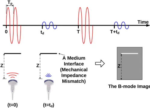
Medical ultrasound systems use different “imaging modes” to assist various diag-noses [8,9]. For visualization of the tissue anatomy, the most common imaging modes include A, B, C and M modes [9, 10]. The B-mode is the most common mode and its typical operation is shown in Figure 2-1. The imaging system uses a 1D transducer array and pulsed ultrasonic waves to probe the tissue medium, in order to acquire a 2D grayscale image of the tissue. At time 0, the transmitter circuit drives the transducer to emit the ultrasonic pulse as shown by the red pulse. The pulse travels through the tissue at the sound speed c, typically 1540m/s in human soft tissue [16]. When it hits some medium interfaces, the mechanical impedance mismatch at each interface generates reflected ultrasonic waves. An interface at depth Z leads to a
Time 0 td T T+td Z A Medium Interface (Mechanical Impedance Mismatch) Tp Z (t=0) (t=td) Z
The B-mode Image
Figure 2-1: The typical signals and the operation for B-mode ultrasound.
received ultrasonic echo at time td = 2Z/c, as shown by the blue pulse. Because
the echo amplitude is proportional to how large the mechanical impedance mismatch is, the amplitude information is translated to the grayscale intensity of pixels in the image. Meanwhile, the time delay from the received echo to the transmit instance (td)
translates to the depth, indicating the interface location in the image. A simplified grayscale image is also shown in the figure.
The transmit-receive action is repeated after time T , such that the B-mode image can be continuously updated in time. The period T is called the pulse repetition period (PRP), and it needs to be long enough to ensure that all ultrasonic echoes from the previous transmission are back. Given that the ultrasonic wave travels at the sound speed of about 1540m/s and the typical image depth of 7.5cm, one transmit-receive repetition will take approximately 100µs (2 × 7.5cm ÷ 1540m/s = 97µs). The reciprocal of PRP is called the pulse repetition frequency (PRF), which is the number of pulses per second. It is a term frequently used in active imaging systems such as the ultrasound, sonar or radar systems. A typical PRF in ultrasound is 10kHz corresponding to the 100µs PRP. Depending on applications, commonly used PRFs can be from 5 to 20kHz.
The red transmit pulse shown in Figure 2-1 is composed of 2 bursts of sinusoids with a cycle period of Tp. While it shows a typical case, the sinusoidal pulse shape
can be replaced by other pulse shapes, such as discrete level pulses, which will be discussed in this thesis. The number of bursts in one transmission can also be variable depending on applications. Generally speaking, more bursts lead to stronger reflected echoes, while less bursts lead to better image axial resolution because of the shorter pulse duration. B-mode imaging commonly employs 2-5 bursts per transmission; and PW Doppler imaging (see next paragraph) employs as many as 20 bursts to improve signal strength in the received echoes.
Besides direct visualization of tissue anatomy, the Doppler effect is used to ob-tain blood flow velocity information inside human body [17]. There are mainly three Doppler modes: Continuous Wave (CW), Pulsed Wave (PW) and Color Flow Mode (CFM) Doppler [11–15]. The CW Doppler is the earliest mode, which transmits con-tinuous ultrasonic waves into human body and detects Doppler frequency shift from the echo waves [13]. It is simple and reliable, but lacks range information. The PW Doppler improves upon the CW mode by repeatedly sending pulsed ultrasonic waves into the medium [14]. The time of flight of the received echoes contains the range information, and the slight timing difference between consecutive echo pulses reflects the object movement1. Sub-sampling at the PRF is usually carried out before the
spectrum analysis for the PW Doppler frequency shift [11]. The CFM Doppler is used to present velocity information as a color-coded image, which is often overlaid on top of a B-mode image. Time-domain autocorrelation based signal processing techniques are often used to speed up the CFM processing [15]. The velocity estimation accuracy is good enough for color-coded visualization.
Many more imaging modes exist. For example, the Harmonic Imaging mode uses the second harmonic of the pulse to provide high resolution images [18–22]; the Power Mode Doppler visualizes the magnitude of Doppler signal, rather than the frequency
1It is important to point out that in the PW mode, the Doppler effect does not come from the
frequency shift of a single received echo pulse, since a short pulse is broadband, and therefore it is difficult to detect the small Doppler frequency shift (typically less than 100KHz). Besides, the frequency-dependent attenuation through the tissue complicates the task even more. Instead, it is the velocity-dependent time delay across several pulses, that carries the velocity information.
!.!,/' !$$%2 /54054 3)'.!, 6!2)!",% $%,!93 !22!9 &/#!, 0/).4 !$#
Figure 2-2: Simplified block diagram of a ultrasound BF system, figure courtesy of [27].
shift, to help identify the existence of low flows and velocities [23]. Furthermore, many imaging modes are used together as Duplex or Triplex modes for the best visualization [24, 25].
2.2
The Beam-formation Principle
Beam-formation (BF) is heavily involved in ultrasonic imaging, to increase the signal-to-noise ratio (SNR), to focus the ultrasound beam to deliver more power, and to steer the beam to scan the imaging space [8, 9, 12, 26, 27]. The beamforming algorithms are based on the delay-and-sum principle, which is shown in Figure 2-2. When a focus is specified, delays are calculated for each ultrasound channel, so that the pulses from different channels travel the same distance between the corresponding transducer elements and the focus.
The implementation of beam-formation can be either analog or digital, and the beam-formation can be achieved at both the transmitting and receiving paths. Be-cause of the denser integration, higher flexibility, and lower power consumption, dig-ital beamforming is favored in modern systems.
Ultrasonic imaging systems are often operating at both the near field (or Fresnel zone) and the far field (or Fraunhofer zone) regions [28–30]. For a round-shape, non-focused, single element transducer, the boundary between the near field and the far
field regions is usually defined at2:
L = D
2
4 · λ, (2.1)
in which the D is the diameter of the transducer surface and the λ is the ultrasound wavelength.
In the near field, the pressure amplitude varies drastically, with many local max-imums and minmax-imums. This complex characteristic is caused by the constructive and destructive interference wave patterns of ultrasound beam. In the far field, the pressure amplitude decreases monotonically with distance and the ultrasound beam diverges at the angle θ defined as: sin (θ) = 1.22Dλ.
At the boundary of the near and far field, where the distance is roughly given by Equation (2.1), the maximum pressure amplitude, or equivalently the maximum ultrasound intensity, is reached; and the beamwidth is minimized at the same time. According to [28–30], the effective beamwidth is approximately equal to half of the transducer diameter D; the pressure amplitude is therefore about 2 times of the pressure amplitude at the transducer surface.
Because of this unique property, it is advantageous for ultrasonic imaging to op-erate close to the near and far field interface, for best SNR and lateral resolution. As a simple numerical example, a typical single element transducer for an intracranial pressure (ICP) measurement has a diameter of about 1.5cm [32, 33]. The typical op-erating frequency is 2MHz and the typical ultrasound speed in human soft tissue is 1540m/s [16], giving a wavelength of 0.77mm. The interface distance calculated from Equation (2.1) is therefore 7.3cm, which is about the same distance from the target brain blood vessel to the transducer3.
Because the system operates heavily in near field region, time-domain techniques for beamforming and processing are common in ultrasonic imaging. Consequently,
2Depending on applications, there are many different definitions [31]. The one used in this article
is most widely used in medical ultrasound area.
3For transducers with more complex shapes and structures, the equations presented above will
be slightly different by some factors. But the effective aperture size D can be used to approximate the element diameter, and the conclusions about near field and far field more or less stay the same.
the ultrasound pulses are short-duration, wideband signals to facilitate time based algorithms.
In additional to the basic delay-and-sum beam-formation principle, several tech-niques are often used to improve the visualization, creating a more homogeneous image quality throughout the full depth [8, 9, 12]. They have been applied to imaging experiments of our work.
• Dynamic focusing: Instead of a fixed array delay pattern for a fixed focal point in the space, the dynamic focusing technique implements a continuously moving focal point across different imaging depth. The array elements are con-trolled to focus signals at a shallow depth at the beginning; as time progresses (corresponding to depth increase), the array delay pattern is gradually modified to move the focal point into deeper depth until the end of the imaging depth. Compared to a single focal point, dynamic focusing generates high detail res-olution and high contrast resres-olution for all depths. It can be relatively easily implemented by a digital beamformer at the receive side.
• Constant F-number imaging: F-number (F #) is the ratio of focal length (f ) to the imaging aperture diameter (D), as in (2.2).
F # = f
D. (2.2)
It is an important concept in optics, photography, and ultrasound. In ultra-sound, the constant F-number imaging technique keeps a constant F # by grad-ually enlarging the active aperture (D) as the focused imaging depth (f ) grows larger. The result of this technique is a constant lateral resolution and it is often used in conjunction with the dynamic focusing technique.
2.3
Ultrasonic Transducers
Currently, 1D ultrasonic transducer arrays for 2D medical ultrasound images is the common practice [8, 12, 34–36]. The transducer arrays are usually built with
piezo-electric materials. Element count of an array can be as high as one thousand. The interconnection to the electronics are co-axial cables.
3D ultrasonic imaging can be achieved by translating or rotating a 1D transducer array over the space [3, 4], but the accuracy and speed is limited by the mechanical movements. As a result, 2D transducer arrays and the supporting 2D electronics are more desirable for 3D ultrasonic imaging. There are commercial 3D imaging systems utilizing 2D transducer arrays. For example, Philips Matrix X6-1 is a 2D array that contains 9,212 elements [37]. However, cables are still needed for the interconnections between the transducer probe and the data acquisition system, which might not be the best solution for 3D imaging, due to the high channel count. Additionally, the 2D transducers have been built from piezoelectric materials [37,38], where manual dicing is often needed to separate individual array elements. The interconnection and yield problems are challenging as the array gets larger and the element size gets smaller.
The capacitive micromachined ultrasonic transducer (CMUT) [39–41] is an alter-native to the traditional piezoelectric transducers (PZTs). The CMUT technology of-fers advantages such as improved bandwidth, ease of fabricating large arrays, and po-tential for integration with electronics with the through-silicon vias (TSVs) [40,42,43] or monolithic CMUT-CMOS integration [44–46].
But there are also challenges for CMUT. Most importantly, the output power and efficiency are still relatively low, partly due to the large parasitic device capacitance. The primary reason for the large parasitic capacitance is the physical structure of the CMUT element, which forms a parallel-plate capacitor [41]. As a result, the transmitter and receiver circuitry that interfaces to CMUT is different from that for PZT. They need to be designed appropriately to prevent excessive performance degradation caused by the load that is much more capacitive and higher impedance. The piezoelectric micromachined ultrasonic transducers (PMUTs) also emerge as another possible 2D transducer solution for 3D imaging [47–51]. It combines the piezoelectric material with micromachining techniques, trying to exploit the benefits from both worlds. The piezoelectric material tends to provide transduction with relatively high efficiency and good linearity, while the micromachining process helps
create fine-pitched 2D arrays with higher yield and reliability. As a technology in its early research phase, it has shown initial success of a 5x5 working array [47]. More works are being done to address problems with this technology, including how to enhance the device bandwidth to generate images with better axial resolution; and how to reduce the intrinsic device parasitic capacitance from the high permittivity of the piezoelectric material [48, 49, 51].
In this thesis, we design block-level circuits for CMUT, but our architecture and system innovations are not limited to a particular transducer type, as will be discussed in succeeding chapters.
2.4
Field II Simulation Program
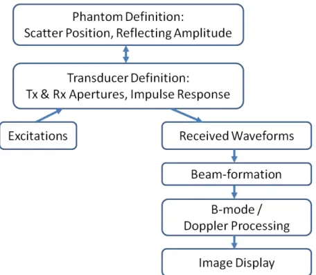
In our work, we make heavy use of the Field II Simulation Program [52, 53] to model the complete hardware and software setup. Field II is a behavioral simulation package running under MATLAB (The MathWorks, Natick, MA) Environment. Figure 2-3 shows a typical Field II simulation flow diagram. The users have the freedom of defining the ultrasonic phantom (i.e. the medium being imaged by the system), transducer property, pulsing / receiving methods, beam-formation algorithms, and image processing / display methods. Based on the user definition, Field II simulates the ultrasound transducer fields and ultrasonic imaging using linear acoustics.
The phantom definition is realized by specifying point scatterers in space with different reflecting amplitudes. It can be a simple single scatterer phantom that characterizes the point spread function of an imaging system; or complex shapes defined by a set of scatterers. Moving structures can also be instantiated by a sequence of phantoms with slight position changes over time, which is useful in simulations for ultrasonic Doppler systems.
The transducers are defined with the type, frequency response and active aperture. The transducer types include 1D, 1.5D, 2D arrays, as well as curved arrays with concave or convex shapes. The transducer element dimensions can be freely specified and the element frequency response is described by its impulse response. Transmit
Figure 2-3: A typical Field II flow diagram for ultrasonic system behavioral simula-tion.
and receive apertures are defined separately, while the active elements are selectable within the array. Two other properties associated with the active apertures are the focus and apodization. Through the focus specification, the beam-formation delays can be automatically calculated for each element in an aperture. The apodization gives amplitude weights for signals at different transducer elements. Both focus and apodization can be a function of time, in which dynamic focusing / apodization is realized.
The pulsing excitation for the transducer is supplied to the array by a time-domain pulse waveform. Based on the pulsation, phantom definition and transducer property, the received echo waveforms from every element in the Rx aperture are produced by the Field II simulator. Beam-formation is performed on the collected echo waveforms; and the beamformed waveforms can then be used to construct a 2D or 3D image, or further processed for Doppler information.
With the ultrasonic field simulation, Field II helps verify the acoustical physics and visually show the ultrasonic pressure field generated by the transducer. With
the capability of incorporating different beam-formation algorithms, it allows the development and validation of new architecture-level and system-level ideas. It could also be used to model non-ideality from circuits and transducers, so that a practical understanding of the real imaging system can be achieved. As will be seen in the following chapters, Field II simulation plays an important role in the thesis work.
Chapter 3
The Column-Row-Parallel
Architecture for 3D Ultrasonic
Imaging
This chapter describes our approach to solve the challenges in realizing a 3D medical ultrasonic imaging system. The analog front-end architectural trade-offs are first dis-cussed and the design process of the Column-Row-Parallel architecture is presented. The implementation of the proposed architecture is then shown, which is both scalable for hardware realization and flexible for software algorithm support. The functionality of the implemented architecture is then described.
3.1
The Prior Art of Architectures for 3D
Ultra-sonic Imaging
A 2D NxN transducer array is often used to acquire 3D volumetric data, where the architecture of the front-end circuit interfacing to the transducer array is an important design consideration.
The most straightforward way to interconnect to a 2D transducer array is to use a fully-parallel architecture, but it is not very scalable for hardware implementation.
A fully-parallel architecture requires N2 active transceivers that are operating at
the same time. As a result, it requires N2 independent input control lines for the
transmitter array and N2 output data lines for the receiver array. As the array size
grows bigger, the required channel count will be correspondingly larger and this is difficult to scale up economically.
On the other extreme, a serialized system could be used to save channel count, but it is usually too slow for data acquisition. One could serialize the input control lines and/or the output data lines of the aforementioned fully-parallel system, so that the number of interconnect lines needed is reduced. Due to the large number of channels to be serialized, the data rate requirement would become too high to be practical, following a similar N2 scaling trend. Alternatively, one could use a
single-channel transceiver to sweep the 2D array, one element at a time. The transceiver is connected to each element by multiplexing and it repeatedly transmits and receives ultrasound with different elements in the array to acquire a full data set [40]. Given that one transmit-receive repetition could take as long as 100µs (Section 2.1), and that the total time consumed to gather one full data set increases with N2 trend, the image frame rate would greatly suffer as the array size continues to grow bigger.
Therefore, to alleviate the conflict between hardware complexity and data acqui-sition speed in 3D ultrasonic imaging systems, there is a lot of research on various sub-array architectures that lie in between the fully-parallel architecture and the se-rialized single-channel architecture. In [43], the diagonal elements in a full 2D array are used to form the receive aperture, while the rest of the 2D elements are used to form the transmit aperture. At the transmitter side, it is close to a fully-parallel architecture because almost all elements are being used. To provide the transmit beam-formation delay pattern for all transmitters, the digital delay values are seri-ally streamed in to program each transmitter. It saves the interconnection but slows down the programming speed. At the receive side, the output channel count is re-duced to N from N2 because only the diagonal sub-array elements are used. This diagonal sub-array approach leads to an elevated side-lobe level that degrades the image contrast. Similarly, [54] investigated possibilities of various sparsely sampled
Figure 3-1: Column-parallel architecture implementations in the literature: (a) a 1D transducer array mechanically translated to scan the 3D space, elevation beam-formation is done by a synthetic virtual source technique, figure courtesy of [3]; (b) a 2D array operated to receive row-by-row, elevation beam-formation is done by sub-array delay-and-sum across the column using analog delay lines, figure courtesy of [55].
2D aperture patterns. But because the sub-array is fixed once the pattern is chosen, the reduction of active elements generally leads to higher side-lobes and worse image resolution performance.
To avoid a fixed sub-array pattern selection, another sub-array idea of using either 3x3 or 5x5 elements is described in [37]. The sub-arrays are programmable and each sub-array performs beam-formation to compress the received data into one channel, reducing the overall channel count by a factor of 9 or 25. To maintain the image quality and avoid introducing artifacts, programmable delay patterns for the sub-array are required. This requirement directly translates into analog delay lines in a hardware implementation, which tends to be bulky and power hungry.
In [3, 4], a conventional 1D transducer array is used as a sub-array and is me-chanically translated or rotated to achieve synthetic 3D imaging, as shown in Figure 3-1(a). The active channel count is reduced to N and the synthetic beam-formation technique could produce good image quality, as long as the object being imaged is static or moving at a much slower speed than the image frame rate, to avoid
mo-tion artifact. The major drawback in this solumo-tion is the mechanical implementamo-tion, which is both a bottleneck for frame rate due to the slow movement speed, and a bot-tleneck for power saving due to the large amount of power needed to drive a motor. More recently, to replace the mechanical translation, an electrical scanning front-end architecture is implemented as shown in Figure 3-1(b) [55–57]. The receiver channels are turned on row-by-row to collect reflected ultrasound echoes. By activating differ-ent rows of transducer elemdiffer-ents over consecutive ultrasound transmits, it effectively mimics the translation of a 1D transducer array, but much faster and lower power.
3.2
The Motivation of the Column-Row-Parallel
ASIC Architecture
The work in [3] and [56, 57] both employ row-by-row (i.e. column-parallel) operation to reduce number of active channels from N2 to N . The 3D image quality from the column-parallel architecture is very good in the azimuth (X) direction because each row can perform full beam-formation along the azimuth direction. However, the beam-formation along the elevation (Y) direction is poor. Techniques such as synthetic virtual source [3] are used to enhance the focusing in elevation with limited success in Figure 3-1(a). Analog delay lines are also attempted to realize elevational beam-focusing to achieve good imaging performance in Figure 3-1(b) [55]. But for the same reason mentioned in the previous section, the analog delay lines lead to large power and silicon area overhead, making system integration difficult.
To cover both azimuth and elevation directions for 3D volumetric imaging, a column-row addressing scheme has been implemented for a 2D transducer design as shown in Figure 3-2 [38, 58–60]. By dicing the transducer top plate row-by-row and dicing the bottom plate column-by-column, the transducer can be driven row-by-row in transmit (Figure 3-2(a)) and column-by-column in receive (Figure 3-2(b)). The combined “Maltese cross” shaped beam-pattern (Figure 3-2(c)) makes it suitable to carry out beam-formation both in azimuth and elevation directions. At the same
Figure 3-2: The column-row addressing scheme implemented on a 256x256 2D trans-ducer array: (a) row-by-row transmit addressing; (b) column-by-column receive ad-dressing; (c) the “Maltese cross” beam-pattern. Figure courtesy of [38].
time, the interconnection complexity for the array is still kept at a linear growth (2*N).
The column-row addressing implemented on the transducer-level has shown po-tential to be a balanced architecture solution for both good image performance and hardware scalability. However it still suffers from a lack of flexibility, because the transducer array is hard-wired to be divided into rows and columns. The limitation of only addressing the elements by one row or one column at a time provides limited freedom for the supporting algorithm design. On the other hand, if one could im-plement a similar column-row addressing architecture at the circuit-level instead of at the transducer-level, as depicted in Figure 3-3, the element addressing mechanism could be much more flexible. With the highly programmable control support from the electronics, various sub-array patterns could be possible on the same system, allowing more versatile functionality and more design freedom at the system-level.
Figure 3-3: A column-row addressing architecture implemented at the circuit-level, with column and row interconnections that reduce the system channel count and provide maximum flexibility for algorithms.
3.3
The Column-Row-Parallel ASIC Architecture
In our work, a Column-Row-Parallel architecture is implemented at the circuit-level with much more diverse functionality and a better trade-off between complexity and speed. Figure 3-3 in the previous section is a conceptual drawing of the proposed architecture, while Figure 3-4 shows a detailed picture. 2D CMUTs are chosen as the target transducer arrays for this work, because of its ease of integration and scalability [39, 40, 43]. But the same architecture design can be applied to other types of 2D ultrasonic transducers easily.
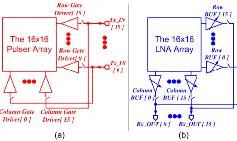
As shown in Figure 3-4, a 2D CMUT (16x16 transducer arrays are used in this work) is DC biased at 30-50V from the common top membrane and each CMUT element’s bottom pad is connected to its corresponding ASIC channel. The DC bias network is provided off-chip with the resistor and the capacitor being shared across all CMUT elements in the array [40, 41]. As indicated by both Figure 3-3 and Figure 3-4, there is a transmitter (Tx) pulser, a receiver (Rx) low noise amplifier (LNA), and a receiver high voltage (HV) protection switch per electronic channel, under each
Shared External Biasing CMUT ASIC Gate Dr
Column Select Logic
Gate Dr Delay Gate DrDelay BUF Delay Gate Dr Delay Column Circuitry BUF BUF BUF Rx Rx Rx Rx
Figure 3-4: Column-Row-Parallel architecture block diagram, the CMUT and ASIC chips are stacked vertically.
CMUT element. The total silicon layout area of a transceiver is designed to be the same as a CMUT element’s area, which is 250µm × 250µm in this work, so that the ASIC channels can be element-matched to the CMUT pitch. The Tx pulser gate drivers and Rx buffer amplifiers are placed at the ASIC perimeter to interface to the transceiver array. There are 16 copies of Tx drivers and Rx buffers at the column side and another 16 copies at the row side, reducing the ASIC I/Os down to “N ”1.
Zooming into one transceiver channel located at ithcolumn and the jthrow, Figure
3-5 shows that Tx and Rx operations are independent and time-multiplexed. The control inputs of the transceiver channel include: the ith column select signals (T c[i],
Rc[i]) supplied from the column side, the jth row select signals (T r[j], Rr[j]) from the row side, and the local per-element enable bits (T en, R en). The column and row select signals are designed to be only active at one side, they cannot be asserted at the same time. The signals are input to the per-element logic unit, shown in Figure 3-5(b), to generate corresponding internal switch controls including: T r, T c, Rr, Rc, and RxSw.
T r and T c determine whether the Tx pulser is driven by the column side or the row side, or none, in which case the pulser is turned off. When the Tx element [i, j] is enabled (T en = 1) and the jth Tx row is selected (T r[j] = 1), the internal switch
control signal T r becomes high and the Tx pulser gate drive signals are supplied from the Column Gate Driver[i]. The array’s Tx path is in column-parallel mode. When the Tx element [i, j] is enabled (T en = 1) and the ith Tx column is selected
(T c[i] = 1), the internal switch control signal T c becomes high and the Tx pulser gate drive signals are supplied from the Row Gate Driver[j]. The array’s Tx path is in row-parallel mode. When the Tx element [i, j] is disabled (T en = 0); or when neither Tx row or Tx column is selected (T r[j] = T c[i] = 0), both T r and T c are low and the Tx pulser is turned off, ignoring gate drive signals from both column and row gate drivers.
Similarly, Rr and Rc determine whether the Rx LNA outputs its analog signal to the column side or the row side, or none, in which case the LNA is turned off.
Transceiver
[ i, j ]
Column
Gate Driver[ i ]
Tr[ j ]
Rr[ j ]
Tc[ i ] Rc[ i ]
T RColumn
BUF[ i ]
Row
BUF[ j ]
Row
Gate Driver[ j ]
T_en R_en
T_en Tc[ i ] T_en Tr[ j ] R_en Rc[ i ]+Rr[ j ] R_en Rc[ i ] R_en Rr[ j ] b bFigure 3-5: (a) The block-level implementation of one transceiver channel and (b) the per-element logic implementation. Column and row select logic is implemented with shift registers that can be reprogrammed in “N ” time (implementation detail will be shown in Figure 5-2).
When the Rx element [i, j] is enabled (R en = 1) and the jth Rx row is selected
(Rr[j] = 1), the internal switch control signal Rr becomes high and the Rx LNA output is connected to the Column Buf f er[i]. The array’s Rx path is in column-parallel mode. When the Rx element [i, j] is enabled (R en = 1) and the ith Rx
column is selected (Rc[i] = 1), the internal switch control signal Rc becomes high and the Rx LNA output is connected to the Row Buf f er[j]. The array’s Rx path is in row-parallel mode. When the Rx element [i, j] is disabled (R en = 0); or when neither Rx row or Rx column is selected (Rr[j] = Rc[i] = 0), both Rr and Rc are low and the Rx LNA is turned off, presenting as high output impedance to both column and row buffers.
The Rx HV protection switch protects low voltage Rx electronics from high voltage Tx transients. An additional internal control signal, RxSw, is generated to control the gate of the protection switch. Whenever the Rx LNA is activated and connected to either column or row buffer, the HV switch is turned on (RxSw = 1) to allow CMUT signal to reach LNA for amplification. The HV switch is off when the LNA is not activated, and it also remains off during Tx pulsing to isolate the high voltage pulsing transients.
The detailed circuit implementation for generating column / row select signals as well as the per-element enable bits will be the topic of Chapter 5. But as a high-level description, these selection and enable bits are stored in shift registers (SR’s) which can be programmed serially. The column and row select signals are 16-bit long for the 16 columns and rows, while the per-element enable bits are 512-bit long, accounting for 1-bit Tx enabling and 1-bit Rx enabling for each CMUT element in the 16x16 array. Furthermore, two multiplexed banks for each control set are implemented. For example, there are two multiplexed 512-bit SR banks for per-element enable bit programming. One SR bank can be used in normal operation while the other bank is being reprogrammed. Alternatively, two SR banks can be both initiated so that one could quickly alternate between the two banks to achieve fast aperture switching between two pre-defined aperture patterns.
Row BUF [ 0 ] Column BUF [ 15 ] Row BUF [ 15 ] Column BUF [ 0 ] Rx_OUT [ 0 ] Rx_OUT [ 15 ] Row Gate Driver[ 0 ] Column Gate Driver[ 15 ] Row Gate Driver[ 15 ] Column Gate Driver[ 0 ] Tx_IN [ 0 ] Tx_IN [ 15 ]
Figure 3-6: (a) Tx input port multiplexing, implemented with digital logic; (b) Rx output port multiplexing, implemented with analog pass-gates.
column and row circuits share I/O ports by multiplexing, as shown in Figure 3-62.
For Tx, the multiplexing switches are implemented with digital logic gates; for Rx, the multiplexing switches are implemented with analog pass-gates for analog signal outputs. In this way, the input ports for Tx beamforming control and output ports for Rx received waveforms are both 16 instead of 32 for a 16x16 array, saving the chip I/O count considerably. And the chip’s interface scaling trend becomes N (rather than 2N ), which is the same trend as a 1D array for 2D imaging.
3.4
The Functionality of the Column-Row-Parallel
Architecture
In this section, a few examples will be utilized to help understand how the proposed Column-Row-Parallel ASIC architecture could be used for 3D ultrasonic imaging.
Figure 3-7 shows an exemplary configuration of a column-parallel mode Tx aper-ture on the 16x16 CMUT-ASIC system. Note that the exemplary configuration is broken down and illustrated in steps to help understanding, but the actual ASIC
2This implementation detail is not shown in most other block diagram figures to avoid
![Figure 2-2: Simplified block diagram of a ultrasound BF system, figure courtesy of [27].](https://thumb-eu.123doks.com/thumbv2/123doknet/14373783.504771/32.918.173.750.118.336/figure-simplified-block-diagram-ultrasound-bf-figure-courtesy.webp)

![Figure 4-14: The illustration of how PWCC works for 2D ultrasonic imaging, courtesy of [68].](https://thumb-eu.123doks.com/thumbv2/123doknet/14373783.504771/69.918.242.674.111.389/figure-illustration-pwcc-works-d-ultrasonic-imaging-courtesy.webp)
![Figure 4-15: The principle of coherent compounding used in PWCC, courtesy of [68]:](https://thumb-eu.123doks.com/thumbv2/123doknet/14373783.504771/70.918.158.760.112.340/figure-principle-coherent-compounding-used-pwcc-courtesy.webp)