HAL Id: tel-02124529
https://tel.archives-ouvertes.fr/tel-02124529
Submitted on 9 May 2019HAL is a multi-disciplinary open access archive for the deposit and dissemination of sci-entific research documents, whether they are
pub-L’archive ouverte pluridisciplinaire HAL, est destinée au dépôt et à la diffusion de documents scientifiques de niveau recherche, publiés ou non,
Teng Zhang
To cite this version:
Teng Zhang. Deep levels characterizations in SiC to optimize high voltage devices. Electronics. Université de Lyon, 2018. English. �NNT : 2018LYSEI108�. �tel-02124529�
N°d’ordre NNT : 2018LYSEI108
THESE de DOCTORAT DE L’UNIVERSITE DE LYON
opérée au sein de
INSA de Lyon
Ecole Doctorale
N° ED160
Électronique, Électrotechnique, Automatique
Spécialité de doctorat
: Génie ÉlectriqueSoutenue publiquement le 13/12/2018, par :
Teng ZHANG
Caractérisations des défauts profonds
du SiC et pour l'optimisation des
performances des composants haute
tension
Devant le jury composé de :
TARTARIN, Jean-Guy Professeur des Universités Labo. LAAS Président TARTARIN, Jean-Guy Professeur des Universités Labo. LAAS Rapporteur BI, Jinshun Professeur des Universités UCAS, Beijing Rapporteur LOCATELLI, Marie-Laure Chargée de Recherche Labo. LAPLACE Examinatrice JUILLAGUET, Sandrine Maître de Conférences Labo. L2C Examinatrice PLANSON, Dominique Professeur des Universités INSA de Lyon Directeur de thèse
Acknowledgement
Sincere appreciation to my advisors Christophe Raynaud and Dominique Planson, as huge hints along with precious guidance and support have been provided which help me to unlock the door to the physics throughout these 3 years of my PhD study that is worshipful.
In addition, I’d like to acknowledge my dear colleges in laboratory Ampère, INSA who helped a lot: R. Caillaud, S. O. Avino, S. Niu, B. Asllani, M. Beye el al., as well as enlightening professors such as B. Allard and G. Bermond. Thanks to my friends of China namely B. Yu, C. Zhou, X. Wang, B. Cuan, X. Jiang, C. Xu, X. Zhu, Y. MA, F. Liu, Y. Li et al. as well for the skylark.
Remarkable acknowledgment to the Labo Ampère, INSA de Lyon, and the CSC also quenching any menace from the “rear” that could come across to me: from delicious menu I appreciate a lot, basic funding for the comfortable lives, to the well-designed curriculum enlarging my knowledge about the fundamental modern theory and keeping my brain CPU lighting for overcoming those struggles that block the road to scientific accomplishment.
At last, I would like to give my sincere and special to my family for supporting the journey for studying in France, the one that had been attracting me a lot, and this footmark I left in Lyon and INSA is so glittering that will never come to the ennui.
Abstract
Due to the increasing appeal to the high voltage, high temperature and high frequency applications, Silicon Carbide (SiC) is continuing attracting world’s attention as one of the most competitive candidate for replacing silicon in power electric field. Meanwhile, it is important to characterize the defects in semiconductors and to investigate their influences on power devices since they are directly linked to the carrier lifetime. Moreover, reliability that is also affected by defects becomes an unavoidable issue now in power electrics.
Defects, including point defects and extended defects, can introduce additional ener-gy levels in the bandgap of SiC due to various metallic impurities such as Ti, Fe or intrin-sic defects (vacancies, interstitial…) of the cristalline lattice itself. As one of the widely used defect characterization method, Deep Level Transient Spectroscopy (DLTS) is supe-rior in determining the activation energy EA, capture cross section and defect
concen-tration NT as well as the defect profile in the depletion region thanks to its diverse testing
modes and advanced numerical analysis.
Determination of Schottky Barrier Height (SBH) has been confusing for long time. Apart from experimental measurement according to I-V or C-V characteristics, various models from Gaussian distribution of SBH to potential fluctuation model have been put forward. Now it was found that these models are connected with the help of flat-band bar-rier height BF. The Richardson plot based on BF along with the potential fluctuation model becomes a powerful tool for SBH characterization. SBHs with different metal con-tacts were characterized, and the diodes with multi-barrier are verified by different models. Electron traps in SiC were studied in Schottky and PiN diodes, while hole traps were investigated under strong injection conditions in PiN diodes. 9 electron traps and 4 hole traps have been found in our samples of 4H-SiC. A linear relationship between the extract-ed EA and log( ) indicates the existence of the intrinsic temperature of each defects.
However, no obvious difference has been found related to either barrier inhomogeneity or contact metal. Furthermore, the electron traps near interface and fixed positive charges in the oxide layer were investigated on SiC power MOSFETs by High Temperature Gate Bi-as (HTGB) and Total Ionizing Dose (TID) caused by irradiation. An HTGB-Bi-assist-TID model was established in order to explain the synergetic effect.
Two carrier freeze-out regions were found near 40 K and 100 K that will degenerate the accuracy of traditional capacitance DLTS test. Meanwhile, concentration of certain de-fects can be reduced by high temperature annealing, that is also a cause to the multi-barrier effect. Special attentions were paid on defects with tiny activation energy at extremely low temperature as well as the abnormal DLTS signal caused by negative-U centers. Irregular switch on DLTS transient (i.e. between capture and emission) is found related to width of detection zone in depletion region.
Abstract
Future works are mainly focused on interface characterization as well as improve-ment on trapping models at low temperature. In addition, the stress effect especially intro-duced by the characterization method should be paid attention as well.
List of figures
Figure 1.1. Comparison of material properties of Si, SiC and GaN [3]. ... 5 Figure 1.2. Major territories of individual unipolar and bipolar power devices for Si
and SiC in terms of the rated blocking voltage [13]. ... 7 Figure 1.3. Double barrier phenomenon in Schottky diode. ... 8 Figure 1.4. Temperature dependence of forward I-V characteristics for 4H-SiC
rectifier reported in [19]. ... 9 Figure 1.5. Number of articles which report defects with certain activation energy
(ECET) in 4H-SiC. ... 13 Figure 2.1. Formation of an ideal Schottky barrier between a metal and an n -type
semiconductor (a) neutral and isolated, (b) electrically connected by a wire, (c) separated by a narrow gap, (d) in perfect contact. Cross and circle marks in (b) denote donor ion and electron in conduction band respectively. ... 16 Figure 2.2. Metal-semiconductor contact with interface states. ... 17 Figure 2.3. Main current transport processes in a forward-biased Schottky barrier. .. 19 Figure 2.4. Image-force lowing of SBH. ... 23 Figure 2.5. (a) Schematic of the Tung model. A random distribution of circular patches
of size R0 and barrier height 0
B
in the otherwise homogeneous background of SBH 0
B
. (b) A patch of size comparable to or smaller than the semiconductor Debye length gives rise to a potential sa ddle-point S beneath the patch center O. (c) Potential profile along the interface normal (along O -S) for zero applied bias
a
V , and for a reverse bias (Va0). Reverse bias reduces the potential maximum (i.e., an increased depth) near S. (d) Lateral profile of the potential maximum projected normally onto the MS interface. The dashed line is the exact potential, the dash-dot line is Tung’s parabolic approximation, and the solid line is the truncated paraboloid used to calculate the microscopic BHD. (e), Calculated probability density for a single low-barrier patch of strength , with
min 0 ( ) B B D and max 0 B B [102]. ... 34 Figure 2.6. The barrier height obtained from I-V measurements as a function of
inverse temperature in [86]. ... 35 Figure 3.1. Schematic of electron capture-emission through trap levels. ... 40 Figure 3.2. Lambda shift under either reverse bias or pulse voltage. ... 42
List of figures
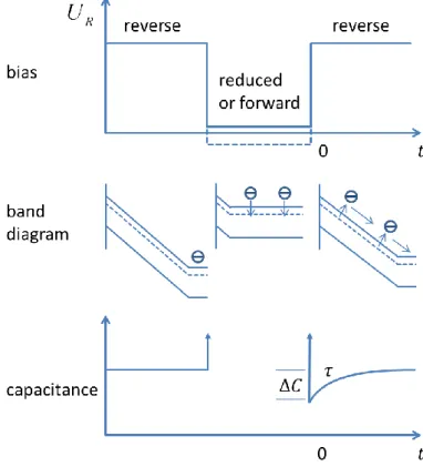
Figure 3.3. A schematic of the DLTS transient signal generation. (a): Steady state reverse bias, (b): Applying pulse; (c): Just after removing pulse; (d): Capacitance transient due to thermal emission of carriers. ... 44 Figure 3.4. Capacitance and band diagram evolution based on bias condition. ... 45 Figure 3.5. Difference in capacitance between two time points at various temperatures
[113]. ... 46 Figure 3.6. Original capacitance transient signal (upper plot) and its Laplace
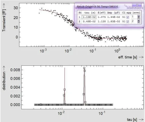
transform spectra (lower plot). Inner table lists the extracted parameters of two different levels, where their fitting curve is presented in the upper plot as solid line. ... 49 Figure 3.7. Isothermal DLTS signal (b1) with variation of pulse width logarithmically
on 4H-SiC SBD with metal contact of tungsten. Three signals were measured at different temperature marked in the plot. ... 53 Figure 3.8. Schematic illustration of pulse shape and capacitance transient in DDLTS
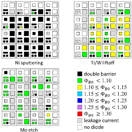
[111]. ... 55 Figure 4.1. Map of cell of SBD samples, diodes within each cell are labeled from D1 to
D6. ... 58 Figure 4.2. Mapping of barrier height on 3 SBD samples. Those marked “no diode” are
lack of effective diodes due to wafer cutting. ... 60 Figure 4.3. Cryostat system used for I-V and C-V measurements. ... 61 Figure 4.4. DLTS test system (left) and its inside view on head part for sample
installation (right). ... 62 Figure 4.5. Forward I-V characteristic on diode Ti/W liftoff. ... 66 Figure 4.6. Calculated Schottky barrier height and shallow doping concentration on
Ti/W liftoff diode based on C-V characterization. ... 67 Figure 4.7. Richardson plot on Ti/W liftoff diode. ... 67 Figure 4.8. Modified Richardson plot and it s modification based on flat-band barrier
height. ... 68 Figure 4.9. Zero-bias barrier height B0 and 1n1 as a function of q 2kT. ... 69 Figure 4.10. Comparison of zero-bias barrier height B0, nB0, SBH determined by
C-V C V and flat-band barrier height BF. ... 69 Figure 4.11. DLTS signal (correlation b1) and the s imulation fitting curve according to
the parameters of 6 trap levels extracted by Arrhenius analysis list in Table 4.6 on Ti/W liftoff diode between 200 K and 550 K. ... 70
Figure 4.12. Current DLTS (I-DLTS) signal (correlation b1) on Ti/W liftoff diode from 70 K to 170 K and between 20 K and 60 K (inner plot), with a period width of 204.8 ms. ... 71 Figure 4.13. Forward I-V characteristics on two diodes (a) and (b) of Mo-etch samples.
... 72 Figure 4.14. Calculated SBH C V based on C-V characterization. Inner plot shows
the extracted doping concentration. ... 73 Figure 4.15. Modified Richardson plot based on the flat -band barrier height BF on
diode (a) and (b). n and IS were calculated in the different linear zones of the I-V curves. ... 74 Figure 4.16. 1n1 as a function of q 2kT on diode (a) and (b). ... 74 Figure 4.17. DLTS signal (correlation b1) with a period width of 204.8 ms on the
diodes (a) and (b) of Mo sample between 200 K and 550 K. The inserts are I-DLTS spectrum between 20 K and 60 K (top right) and 70 K to 170 K (top left). 75 Figure 4.18. DLTS signal (b1) with a period width TW = 204.8 ms of different scan
cycles on Ti/W sputtering 1 min diode (A). ... 76 Figure 4.19. Forward I-V characteristic on diode (A) of Ti/W sputtering 1 min between
200 K and 400 K measured during the DLTS test of (a) : 1st scan and (b) : 3nd scan illustrated in Figure 4.18. ... 77 Figure 4.20. Evolution on forward I-V characteristic due to (a):annealing before DLTS
scan with high temperature and (b) room temperature annealing after high temperature DLTS scan on diode (B) of Ti/W sputtering 1 min with labels
illustrated in Table 4.9. ... 78 Figure 4.21. Evolution on forward I-V characteristic due to DLTS scan on diode (B) of Ti/W sputtering 1 min with labels illustrated in Table 4.9. ... 79 Figure 4.22. DLTS signal (b1) with a period width TW = 204.8 ms of different scan
cycles on Ti/W sputtering 1 min diode (B). The labels indicate the number of DLTS scan cycles (Tempscan) marked in Table 4.9. ... 79 Figure 4.23. Isothermal DLTS scan with variation of period width (TW) from 0.6 ms to
3 s on diode (B) of Ti/W sputtering 1 min sample. Labels o f test number are illustrated in Table 4.9. ... 80 Figure 4.24. Forward I-V characteristics between 80 K and 400 K measured in the
cryostat with a step of 20 K on samples of (a): Tungsten (S7); (b):
Titanium/Tungsten (S3); (c): Nickel (S2) and (d): Molybdenum (S8). Sample descriptions are illustrated in Table 4.1. ... 81
List of figures
Figure 4.25. Comparison of forward I-V curve at 80 K, 300 K and 400 K on four SBDs with different metal contacts. ... 82 Figure 4.26. Modified Richardson plot according to flat-band SBH of 4 diodes with
different metal contacts. ... 82 Figure 4.27. (a):1n1 as a function of q 2kT (potential fluctuation model) and (b)
zero-bias barrier height B0 as a function of q 2kT(Gaussian distribution model) on 4 diodes with different metal contacts. ... 83 Figure 4.28. Temperature dependence on (a): zero -bias barrier height B0 and (b): the SBH extracted from C-V C V of diodes with 4 different metal contacts. ... 85 Figure 4.29. Comparison of DLTS signal (correlation b1) between 200 K and 550 K on
4 diodes with different metal contacts. ... 85 Figure 4.30. Comparison of I-DLTS signal (b1) with a period width of 204.8 ms and
temperature range (a): 20 K to 60 K and (b): 70 K to 170 K. ... 86 Figure 4.31. Mapping of defect activation energy compared to the conduction band
and its capture cross section with the help of Arrhenius analysis based on DLTS results on 4 diodes with different metal contacts. Those points circled with dash lines are suggested to originate from the same defect labeled beside. ... 87 Figure 5.1. Forward I-V characteristics on diode (L) from 20 K to 550 K. ... 90 Figure 5.2. (a): Extracted ideal factor n and saturation current I0 at different
temperatures according to linear regions with relatively high current illustrated in Figure 5.1. and (b): plot of
2
0
ln I T as a function of 1/ nT . Three points marked with red circles were those measured at lowest temperatures (labeled beside the circles) and are not involved in the linear fitting. ... 90 Figure 5.3. (a): DLTS spectra under different pulse voltages UP between 20 K and 550 K with Tw204.8 ms, UR–10 V, TP 100 µs. (b) shows the same signals with a
temperature range from 60 K to 90 K. ... 92 Figure 5.4. (a) DLTS spectra under different pulse width from 20 K to 550 K with
Tw204.8 ms, UR–10 V, UP –0.1 V. (b) is the same signals with a temperature
range from 60 K to 85 K. ... 93 Figure 5.5. DLTS spectra (20 K – 550 K) with three different period widths for (a):
strong hole injection with UP–0.1 V and (b) weak hole injection with UP –2 V.
Other parameters are as follows: UR–10 V, TP 100 µs. The flat area with no
Figure 5.6. I-DLTS signal with a period width of 204.8 ms of both weak and strong injection condition for the PiN diode within the temperature range of (a): 20 K – 60 K and (b): 60 K – 200 K. ... 94 Figure 5.7. HERA analysis results for the defect between 250 K and 450 K, the
extracted level 1 and 2 indicate the possible overlap of the trap levels. ... 97 Figure 5.8. (a): Original threshold voltage for all 20 samples involved in HTGB t est
and (b): Dispersion of normalized Vth before (left part) and after HTGB (right part), with 10 MOSFETs for each group (162 h or 332 h). The first 10 samples (ID R2201 to R2210) belong to 332 h HTGB test and the rest 10 are in the 162 h group. Normalized Vth was separately calculated. ... 100 Figure 5.9. Input capacitance Ciss as a function of applied drain-source voltage Vds on
162h-HTGB device (R2217) and 332h-HTGB device (R2207) before and after HTGB along with data measured after room temperature annealing for a week. ... 100 Figure 5.10. Time dependence of normalized threshold voltage during one week after
HTGB. No bias was added during this annealing at room temperature. ... 101 Figure 5.11. Threshold voltage shift as a function of radiation dose with different
HTGB time, compared to the value right before the radiation experiment. Open symbols present data measured after annealing. X-axis is slighted adjusted within each TID dose group for better reading. ... 101 Figure 5.12. Drain-source leakage current @Vds = 1200 V and the shift on threshold
voltage as a function of radiation dose and HTGB time. Several Idss much lower in 1 kGy group are not shown here. Open symbols present data measured after annealing and the half-filled symbols are the threshold shift compared to their original values. X-axis is slighted adjusted within each TID dose group for better reading. ... 102 Figure 5.13. Gate leakage current @V = 22 V as a function of radiation dose and gs
HTGB time. Open symbols present data measured afte r annealing. X-axis is slighted adjusted within each TID dose group for better reading. ... 103 Figure 5.14. Normalized input capacitance @Vds = 0.1 V as a function of radiation dose and HTGB time. Open symbols present data measured after annealing. X -axis is slighted adjusted within each TID dose group for better reading. The insert shows the variation of Ciss due to HTGB before TID. ... 103 Figure 5.15. Illustration of band diagram near interface during HTGB (right) and TID (left), with the marked process (a): electrons directly tunneling and capture (b):
List of figures
electron-hole pairs generation due to irradiation and (c): holes displacement and capture. ... 104 Figure 5.16. (a): pulse capacitance and (b): reverse capacitance with a bias of –10 V
measured during DLTS scan between 20 K and 550 K on PiN diode discuss ed in section 5.1... 106 Figure 5.17. DLTS signal and the peak analysis by Origin on (a): diode (L) with TP = 1 ms, TW = 100 ms and (b): diode (S) with TP = 1 ms, TW = 200 ms between 80 K and 400 K. The sizes of the Alphabets represent the height of each individual peak. 108 Figure 5.18. Extracted (a): activation energy relate to conduction band ECET and (b):
capture cross section as a function of the test batch with different TP-TW
combinations of peak E on diode (L), along with their correlation on linear fitting during Arrhenius analysis. ... 108 Figure 5.19. Linear relationship between activation energy and capture cross section of
(a): peak E and (b): peak H on diode (L). Two points marked red in (b) are suggested to be the error data and are not used in the linear fitting. ... 109 Figure 5.20. Linear relationship between activation energy and capture cross section of
all three peaks (A, E, and H) on diode (L) and diode (S). Several points of peak H are suggested to be the error data and are marked red. ... 109 Figure 5.21. DLTS signal (correlation b1) with a period width of 204.8 ms on (a): Ti/W
sputtering 1min sample (S4) and (b): Ni sputte ring sample (S2) during
temperature scan in different directions (heat up or cool down). The waiting time between scan of 300 K – 600 K and 600 K – 300 K is limited to minutes and can be neglected. ... 111 Figure 5.22. Signal DLTS on different correlations (a): a1(Tw/2) and (b): b1M on the
Ti/W sample with the same scan 300 K – 600 K – 300 K as in Figure 5.21(a). ... 112 Figure 5.23. DLTS signal (correlation b1) between 300 K and 550 K on PiN diode
discussed in section 5.1 with a period width of 20.48 ms and 2.048 s (top -right plot). Before the DLTS scan 550 K – 300 K, an additional waiting time of 30 min are applied with tiny bias (–0.1 V) right after the heat-up scan (300 K – 550 K). ... 113 Figure 5.24. DLTS spectra with 3 different period wid ths on diode Ti/W liftoff (S3)
between (a): 60 K and 600 K, while (b) is the same signal between 60 K and 120 K in order for better illustration, with UR = –10 V, UP = –0.1 V and TP = 100 µs. 114 Figure 5.25. (a): DLTS spectra (b1) between 60 K and 120 K with 7 different period
Figure 5.26. 3D-plot of Figure 5.25(a). The blue and red dash lines indicate the
evolution trend on two peaks. ... 115 Figure 5.27. I-DLTS signal (correlation b1) on Ti/W sputtering 1 min sample (S4) at
low temperature. The black squares are that discussed in Chapter 4, while the red circles are the focus in this section. ... 117 Figure 5.28. Arrhenius plot from maximum analysis of DLTS on diode S4 at
temperature below 25 K. The pulse width is 5 μs and the bias condition on (a) and (b) are listed inside plot. Some points extracted with maximum analysis that do not belong to these two levels are not shown in the plot. ... 118 Figure 5.29. I-DLTS signal (correlation b1) from ITS period scan at 17.35 K on sample S4 with TP = 5 μs, UR = –5 V and UP = –0.1 V. ... 118 Figure 5.30. I-DLTS signal (correlation b1)of isothermal variation of TP at 17.35 K
with a fixed period width of 200 ms. ... 119 Figure 5.31. I-DLTS signal (correlation b1)of isothermal variation of (a): UP and (b):
R
U at 17.35 K. ... 120 Figure 5.32. I-DLTS signal (correlation b1)of isothermal variation of both UP and UR
with pulse heights keep constant. ... 120 Figure 5.33. I-DLTS signal (correlation b1)of isothermal variation of TP at 17.35 K
with a fixed period width of 1 ms. ... 122 Figure 5.34. I-DLTS signal (correlation b1)of isothermal variation of UP at 17.35 K
with (a): UR = –10 V and (b): UR = –20 V. The pulse width is 30 μs and period width is 1 ms. Inner plot in (a) shows the trap concentration profile calculated based on results in (a). ... 122 Figure 5.35. Left plot : I-DLTS signal (correlation b1)of isothermal variation of TP at
17.35 K with a fixed period width of 200 µs. And right plot: the measured
transient curve at different TP in the left plot. ... 123 Figure 5.36. Left plot : I-DLTS signal (correlation b1)of isothermal variation of UR at
17.35 K with a fixed period width of 200 µs. And right plot: the measured
transient curve at different UR in the left plot. ... 123 Figure 5.37. Relationship between the observed transient curve and UPUR during the
DLTS shown in Figure 5.36. The blue dots surrounded by rad dash square indicate the measured transient signals which correspond to that in Figure 5.36 with the same label. ... 124
List of figures
Figure 5.38. The maxima and minima voltage illustrated in Figure 5.37 as a function of pulse voltage used in the DLTS isothermal variatio n of UR measures. Different voltage sources were used that (a): low voltage module up to 20 V and (b): high voltage module up to 100 V. ... 124 Figure 5.39. The maxima and minima voltage illustrated in Figure 5.37 as a function of
reverse bias used in the DLTS isothermal variation of UP measures. Different voltage sources were used that (a): low voltage module up to 20 V a nd (b): high voltage module up to 100 V. ... 125 Figure 5.40. I-DLTS signal (correlation b1)of isothermal variation of UP and UR at
List of tables
Table 1.1. Main Physical Properties of 3C-, 6H-, 4H-SiC, and Si [10, 11]. ... 6
Table 1.2. The maximum blocking voltage available for some commercial high power SiC devices and their fabricants. Information is updated to August 2018. ... 7
Table 1.3. Classification on defects in crystals. ... 10
Table 1.4. Several defects reported in 4H-SiC. ... 14
Table 3.1. Comparison of different DLTS modes from our DLTS manual, it marks with ‘+’ as good, ‘o’ as medium and ‘-’ as bad. ... 51
Table 4.1. 4H-SiC SBD samples used in this study. ... 58
Table 4.2. Size parameters of diodes illustrated in Figure 4.1. ... 59
Table 4.3. Statistics on each sample from the preliminary I -V charactrization. ... 60
Table 4.4. Typical parameters used for capacitance DLTS scan. ... 64
Table 4.5. Common isothermal DLTS modes. ... 64
Table 4.6. Calculated deep level parameters based on Arrhenius plot by DLTS measurement between 200 K and 550 K and those interpretations. The defects are indicated by the position of the positive peak shown in Figure 4.11. ... 71
Table 4.7. Calculated deep level parameters based on Arrhenius plot by I -DLTS measurement between 20 K and 170 K and those interpretations. The defects are indicated by the position of the negative peak shown in Figure 4.12. ... 72
Table 4.8. Comparison of the parameters of the Gaussian model and the potential fluctuation model. The two parameters B0 and S20 are calculated from the Eq. (2.46) with extraction of the MR plot of Figure 4.15. ... 75
Table 4.9. Measure steps and addition condition on diode (B) of Ti/W sputtering 1 min sample. General measure condition of I-V and DLTS temperature scan are given in section 4.2, while that of Isothermal DLTS tests are illustrated in Figure 4.23. ... 77
Table 4.10. Flat-band SBH and effective Richardson constant of diodes with different metal contacts extracted from MR plot shown in Figure 4.26. ... 83
Table 4.11.Parameters in potential fluctuation and Gaussian distribution model of diodes with different metal contacts extracted from plots shown in Figure 4.27 between 80 K and 400 K. ... 84 Table 5.1. Calculated deep level parameters based on Arrhenius plot by I -DLTS
List of tables
The defects are indicated by the position of the negative peak shown in Figure 5.6. ... 95 Table 5.2. Calculated deep level parameters based on Arrhenius plot by C -DLTS
measurement for both strong and weak hole injection. The defects are indicated by the position of the peak shown in Figure 5.4 and Figure 5.5 with the period width of 204.8 ms, while the activation energy is related to either conduction band (electron traps) or valence band (hole traps). ... 96 Table 5.3. Trap levels identification. The type C or I indicates the measure used (C
-DLTS or I--DLTS), while the (e) or (h) in identification points out the defect type (electron trap of hole trap). ... 97 Table 5.4. Main electric parameters tested and test condition. ... 99 Table 5.5. Maximum time delay between the end of radiation and first characterization
following TID test. ... 99 Table 5.6. Activation energies of common SiC doping impurities summarized in [159].
... 107 Table 5.7. Calculated trap parameters on average based on Eq. (5.4) along with he
slope and intercept of linear fitting of each peak shown in Figure 5.20. ... 110 Table 5.8. Extracted trap parameters on Ti/W and Ni samples with the help of
Maximum (maximum Arrhenius analysis) and HERA analysis. ... 112 Table 5.9. Extracted VI of sample S4 at different temperature according to C-V
List of symbols
A Richardson constant / Amplitude of transient
*
A Effective Richardson constant B Offset during transient
C Capacitance
C t Capacitance as a function of time ( )
C t Capacitance as a function of time after the second pulse of DDLTS C
Amplitude of capacitance transient
i
C
Amplitude of individual capacitance transient
0
C Capacitance before transient
iss
C Input capacitance of MOSFET
R
C Capacitance at reverse bias
D Positive charge state D Negative charge state
0
D Neutral charge state
n
D Diffusion constant of electron
S
D Interface states density Electric field
a
E Activation energy
B Breakdown field
C
E Energy level of conduction band
F
E Fermi level
m F
E Fermi level in the metal
s F
E Fermi level in the semiconductor
g
E Energy gap between conduction band and valence band
eff g
E Measured effective forbidden band gap
(0)
g
E Energy gap between conduction band and valence band at 0 K
V
E Energy level of valence band
n
F Discrete Fourier Transform
i Electric field between metal and semiconductor
max Maximum electric field over the barrier
S Surface electric field T
E Energy level of trap
List of symbols
I t Current as a function of time
0
I Saturation current of p-n junction
dss
I Drain-source leakage current of MOSFET
gss
I Gate leakage current of MOSFET
R
I Current at reverse bias
s
I Saturation current of SBD
J Current density
0
J Saturation current density of rectifier
ms
J Current density from metal to semiconductor
r
J Recombination current density
sm
J Current density from semiconductor to metal
te
J Current density according to thermal emission theory
L Distance intersection Fermi level and trap level
N Number of sampling values
C
N Electron effective density of states
A
N Doping concentration of acceptor
D
N Doping concentration of donor
S
N Shallow doping concentration
T
N Trap concentration
d
Q Net positive charge in the semiconductor
m
Q Negative charge on the surface of metal
ss
Q Net positive charge due to interface state
on R On-resistance S R Series resistance S Effective surface i
S Effective surface of region i.
T Temperature
0
T Parameter involved in T0 effect
P
T Pulse width in DLTS
W
T Period width in DLTS
U Energy between donor and acceptor level in negative-U system
r U Recombination ratio H U Pulse height in DLTS P U Pulse voltage in DLTS P
R U Reverse bias in DLTS V Bias voltage B V Breakdown voltage d
V Difference between B and
0
d
V Difference between B and at balance condition ds
V Drain-source voltage
gs
V Gate-source voltage
I
V Intersection with x-axis of 2
1 C ~V plot during Cr -V analysis
i
V Voltage drop between metal and semiconductor if electrically connected
r
V Reverse bias voltage
th
V Gate threshold voltage of MOSFET
n
X Entropy factor during emission process
i
a Fraction of effective surface of individual region with total contact surface
n
a Cosine coefficient of Fourier transform
n
b Sine coefficient of Fourier transform
1
c Electron capture rate between trap level and conduction band
2
c Electron capture rate between trap level and valence band
n
c Electron capture rate / Complex Fourier coefficient
D n
c Discrete Fourier coefficients
d Distance where the barrier falls by a value of kT q from its maximum
e Electron
1
e Electron emission rate between trap level and conduction band
2
e Electron emission rate between trap level and valence band
n
e Electron emission rate
f t Continuous function of time
k
f Discrete sampling value
h Planck constant
k Boltzmann constant
l Carrier mean free path
m Free electron mass
*
m Electron effective mass
n Electron concentration / Ideality factor
0
n Concentration of free electrons
i
n Electron concentration in intrinsic semiconductor
Tc
List of symbols
Te
n Filled traps during the emission process p Hole concentration
t
p Tunneling probability
q Magnitude of the electron charge
0
t Time between end of charging pulse and the first sampling value v Average thermal velocity
th
v Thermal velocity of carrier
,
th n
v Thermal velocity of electrons
S
v Saturation drift velocity
w Depletion region width
eff
w Effective depletion region width where traps can be detected by DLTS
P
w Depletion region width at pulse voltage
R
w Depletion region width at reverse bias
m
x Position where the maximum value of Schottky potential height is reached
B
Schottky barrier height
B
Average of Schottky barrier height
0
B
Calculated average of SBH based on BF and 2 0
B
Schottky barrier height at zero bias
0
B
Average of Schottky barrier height at zero bias
BF
Schottky barrier height on flat-band condition
,
Bn i
Individual constant barrier height of a series of ideal regions
,
Bn l
Individual constant barrier with the lowest barrier height
eff B
Effective Schottky barrier height involving image-force lowering
C V
Schottky barrier height determined by C-V
i
Reduction on barrier height due to image-force lowering
m
Work function of metal
s
Work function of semiconductor
Effective tunneling constant
Temperature coefficient of band gap
s
Electron affinity of semiconductor
Distance between metal and semiconductor
0
Permittivity in the vacuum
i
Permittivity of the interfacial layer
ir
Relative permittivity of the interfacial layer
s
s
Permittivity of the semiconductor under high frequency
0
Neutral level of interface states
Temperature coefficient of saturation current in p-n junction
Carrier mobility
n
Electron mobility
2
Linearity coefficient of B varies with bias voltage
3
Linearity coefficient of S varies with bias voltage
Capture cross section
n
Capture cross section of electrons
p
Capture cross section of holes
S
Standard deviation in Gaussian distribution
S
Calculated standard deviation in Gaussian distribution based on BF and 3 0
S
Standard deviation in Gaussian distribution at zero bias
Time constant
c
Capture time constant
e
Emission time constant
r
Carrier lifetime within the depletion region
0
Angular velocity involved in Fourier transform
Difference between EF and EC
Table of contents
ACKNOWLEDGEMENT
I
ABSTRACT
II
LIST OF FIGURES
IV
LIST OF TABLES
XII
LIST OF SYMBOLS
XIV
TABLE OF CONTENTS
XIX
INTRODUCTION
1
CHAPTER 1 START OF ART
4
1.1 Background 5
1.1.1 Development of modern power electronics and its limitation 5
1.1.2 Silicon carbide (SiC) 6
1.1.3 Schottky barrier diodes (SBD) 8
1.1.4 Multi-barrier in SBD 8
1.2 Reliability and Defects 10
1.2.1 Classification of defects 10
1.2.2 Defects reported in SiC devices 12
CHAPTER 2 BARRIER HEIGHT DETERMINATION OF SCHOTTKY
DIODES
15
2.1 Energy band diagram and formation of Schottky barrier diode 16
2.1.2 The effect of interface states 17
2.2 Current transport mechanisms though Schottky barrier 19
2.2.1 Introduction 19
2.2.2 The diffusion theory 20
2.2.3 The thermionic-emission (TE) theory 20
2.2.4 Tunneling and Thermionic-Field Emission (TFE) model 21
2.2.5 Recombination in the depletion region 22
2.2.6 Image-force lowering of SBH 23
2.3 Measurement of SBH 25
2.3.1 I-V characteristics 25
2.3.2 C-V measurements 26
2.4 Review on SBH models 27
2.4.1 Ideality factor and zero-bias barrier height 27
2.4.2 T0 effect 27
2.4.3 Gaussian distribution 28
2.4.4 Potential Fluctuation model 28
2.4.5 Flat-band barrier height 29
2.4.6 Modified Richardson plot 29
2.4.7 Relationships between different models 29
2.5 Barrier inhomogeneity in Schottky devices 32
2.5.1 Introduction 32
2.5.2 Parallel diode model 32
2.5.3 Tung’s model 33
2.5.4 Multi Gaussian distribution model 35
CHAPTER 3 DEEP LEVELS DETECTION
36
3.1 Overview 37
3.2 Electron capture-emission mechanism 38
3.2.1 Capture 38
3.2.2 Emission 39
3.2.3 Steady state capture-emission 39
Table of contents
3.2.5 Limitation on trap detection 42
3.3 DLTS Principle 44
3.3.1 Basic DLTS principle 44
3.3.2 Fourier transform and DLTFS 46
3.3.3 HERA DLTS 48
3.4 Category of DLTS 50
3.4.1 DLTS transient modes 50
3.4.2 Isothermal DLTS 52
3.4.3 Other DLTS 54
CHAPTER 4 EXPERIMENTAL STUDY ON SIC SBD
57
4.1 Sample used in this study 58
4.1.1 Overview 58 4.1.2 Preliminary statistics 59 4.2 Measurements setup 61 4.2.1 Hardware setup 61 4.2.2 I-V measurements 63 4.2.3 C-V measurements 63 4.2.4 DLTS measurement 63 4.3 Experimental results 66
4.3.1 Case study: Ti/W liftoff sample 66
4.3.2 Research on diode with multi-barriers 72
4.3.3 Comparison on samples with different metal co ntacts 81
CHAPTER 5 CHARACTERIZATION ON OTHER SAMPLES AND
DISCUSSION
88
5.1 PiN diode 89 5.1.1 Sample overview 89 5.1.2 Experiment setup 89 5.1.3 Static Characterization 89 5.1.4 DLTS characterization 915.2 MOSFET 98 5.2.1 Introduction 98 5.2.2 Experiments setup 98 5.2.3 Experimental results 99 5.2.4 Discussion 104 5.3 Discussion 106 5.3.1 Freeze-out effect 106
5.3.2 Relationship between activation energy and capture cross sectio n of certain
defect level. 107
5.3.3 Annealing effect during DLTS 111
5.3.4 Negative-U center 113
5.3.5 Behavior at extremely low temperature 117
CHAPTER 6 CONCLUSION AND PROSPECTIVE
127
6.1 Conclusion 128
6.2 Perspective 130
Silicon carbide, as one of the well-known potential substitute materials of silicon in power electrics, has been attracting attention due to its high temperature, high power, and high frequency applications. The mature on large size of SiC wafer as well as cutting pro-cess bring hope to the commercial massive production, which in turn speeds up the re-search on SiC as the material of new generation.
Reliability is another vital issue throughout the practical application of power devices, and its importance has becoming more and more prominent. As a consequence, studying the failure mechanism and maintaining high performance of devices especially under harsh environment such as space application have turned into a significant branch of power elec-trics.
The crystal models are widely studied as a fundamental basis in semiconductor re-search. However, it is never possible to find perfect crystal in nature. As all materials are tangible with finite volume, the periodical array of atoms will be destroyed at the boundary which leads to large friction of broken bonds near material surface. In addition, other things such as impurities or stress that occur during the growth or formation of the crystal can contribute to the departure from the perfect crystal as well. Furthermore, the process of device fabrication (cutting, polishing, doping, etching etc.) will also introduce the defect in the semiconductor crystal with no doubt. Defects can not only result in degradation on per-formance of power semiconductor devices, but could also lead to the destruction under certain circumstances. On top of that, the impact on those optical devices such as LED chips due to defects should not be ignored. Since those defects and the related trap levels are inevitable, the improvements on the semiconductor process technology have never stopped in order to get rid of the disadvantages as much as possible. On the other hand, doping is one of the most widely used technologies for changing the conductivity by modi-fying the free carrier concentration. Moreover, carrier life time has to be carefully con-trolled in some bipolar devices though introduced trap levels as recombination centers. Therefore, it is significant to make use of imperfect crystal and study the effects due to the trap levels.
This work mainly focuses on the investigation of deep levels in the 4H-SiC power devices, especially their influence on Schottky barrier height. The thesis is organized as follows.
Chapter 1 gives a brief introduction on development of wide band gap SiC power de-vices as well as the multi-barrier effect discovered in those Schottky barriers. Meanwhile, the classification of defects is discussed and a review is given on those defects reported in 4H-SiC with DLTS measurement
Chapter 2 is an introduction of Schottky contact, including the basic structure, current transportation mechanisms, determination and measurement of barrier height. A review on different models related is given and their relationships are discussed as well as those models on barrier height inhomogeneity.
Chapter 3 focuses on deep levels detection, especially on behalf of DLTS measure-ment. After a review on basic theory of capture, emission and transient due to trap levels,
Introduction
DLTS principle is mainly introduced as well as either different category of DLTS or their optimizations.
Chapter 4 is dedicated to the experimental results on SiC Schottky diodes with either static measurements (I-V and C-V) or DLTS test within wide temperature range. Follow-ing a typical case study of Ti/W SBD, the comparison on both sFollow-ingle/multi barrier diodes and SBDs with different metal contact is presented. Furthermore, the evolution of barrier height on Ti/W sputtering sample is discussed.
Chapter 5 provides the study on PiN diodes as well as the influence of irradiation on MOSFETs. Some effects revealed during the experiments are discussed such as freeze-out and annealing on high temperature. The behavior at extremely low temperature is explored as well.
Chapter 1
Start of art
1.1 Background
1.1 Background
1.1.1 Development of modern power electronics and its
limitation
After invention of the first transistor fabricated with germanium in 1947, Ge had been considered as the most useful material for semiconductor technology the following decade until 1960s, when Silicon replaced germanium thanks to its superior thermal stability, reli-able oxide and abundance [1]. From then on, the semiconductor industry has been entering a golden, not only specifically in the evolution on integrated circuit which influences eve-rywhere in our daily lives, but also in the various inventions of power devices such as PiN diode, Vertical Diffused Metal Oxide Semiconductor Field Effect Transistor (VDMOS), Insulated-Gate Bipolar Transistor (IGBT) and their derivatives.
Even though nowadays most of the commercial power semiconductor devices such as VDMOSs or IGBTs are silicon-based, the performance of these Si devices is facing their limitation in power applications owing to the material properties. As an example, the well-known ‘silicon limit’ that describes the relationship for high power MOSFET between the on-resistance Ron and its breakdown voltage VB can be presented as: [2]
9 2.5
5.93 10
on B
R
V
(1.1)Therefore the Ron will increase dramatically at high voltage application, which is
al-ways the problem when it comes to the unipolar device like Schottky diode. Even if this drawback can be overcame by either bipolar device such as IGBT or special structure like Super Junction, the storage of minority carriers in bipolar devices as well as the complicate manufacturing process of novel structure should still be challenging. As a result, it is sig-nificant to turn to those new generation after-silicon materials.
As shown in Figure 1.1, the breakthrough of wide bandgap semiconductor material made by silicon carbide (SiC) and gallium nitride (CaN) brings hope for the development of a new generation of power electronics thanks to their superior characteristics relate to high power application compared to silicon. And these new generation materials have been attracting more and more attentions in the power field.
1.1.2 Silicon carbide (SiC)
Silicon carbide, as was first discovered by Jons Jakob Berzelius in 1824 [4], is one of the attractive semiconductors for high temperature, high power, and high frequency appli-cation [5]. The commercial value of SiC has been discovered early days such as abrasive, high-temperature ceramics and fireproofing thanks to its advantages in either hardness or melting characteristics [6]. Soon it has emerged as the most mature of the wide-bandgap semiconductors since the release of commercial 6H-SiC bulk substrates in 1991 and 4H-SiC substrates in 1994 [7]. As is shown in Table 1.1, 4H-SiC is superior to Si especially for power device application due to its large bandgap, high breakdown field and high thermal conductivity. As a result, the SiC devices can benefit from higher blocking voltage, lower on-resistance, reduced leakage current and higher operation temperature/frequency com-pared to that made by Si. Therefore, silicon carbide is an ideal alternative to silicon for de-vices over 10 kV, as shown in Figure 1.2. A great deal of SiC dede-vices with ultra-high breakdown voltage have been reported such as 15~20 kV 4H-SiC IGBTs [8] and 20 kV 4H-SiC gate turn-off thyristors [9].
Table 1.1. Main Physical Properties of 3C-, 6H-, 4H-SiC, and Si [10, 11].
Properties 3C-SiC 6H-SiC 4H-SiC Si
Energy gap: E eVg( ) 2.4 3.0 3.2 1.12 Electron mobility: 2 ( ) n cm VS 1000 500 1000 1350 Breakdown field: 6 ( ) 10 BV cm 2 2.5 2.2 0.25 Thermal conductivity(W cm C ) 5 5 5 1.5
Saturation drift velocity: 7
( ) 10
S
v cm s 2.5 2 2 1
Maximum operating temperature(C) 1240 1240 1240 300
The crystal lattice of SiC is recognized as closely packed silicon-carbon bilayers (or Si-C double layers), which can be regarded as the alternately arranged planar sheets of sil-icon or carbon atoms. Due to the variation of stacking sequences, different polytypes can be presented. Among over 150 polytypes found in SiC, however, only the 6H- and 4H-SiC
1.1 Background
polytypes are commercially available in both bulk wafers and custom epitaxial layers. Be-tween the two polytypes, 4H-SiC is preferred for power devices primarily because of its high carrier mobility, particularly in c-axis direction and its low dopant ionization energy [12].
Figure 1.2. Major territories of individual unipolar and bipolar power devices for Si and SiC in terms of the rated blocking voltage [13].
Apart from those breakthroughs reported from the laboratories, as listed in Table 1.2, lots of commercial SiC power devices are now available on thousand volt class with re-duced on-resistance compared to Si devices. With the development on breakthrough of SiC wafer fabrication and maturity of the process, SiC devices will continue to expend their influences in power field.
Table 1.2. The maximum blocking voltage available for some commercial high pow-er SiC devices and their fabricants. Information is updated to August 2018.
SiC device Blocking voltage Typical Fabricants
MOSFET 1.7 kV Cree, GeneSiC, IXYS, Microsemi, Rohm
SBD 1.7 kV Cree, Microsemi
Thyristors 6.5 kV GeneSiC
IGBT 600 V IXYS
1.1.3 Schottky barrier diodes (SBD)
SiC p-n junctions could suffer a higher forward power loss compared to Si due to its higher built-in voltage. However, this can be avoided by a Schottky structure [14]. Nowa-days, the 4H-SiC Schottky-barrier diodes (SBDs) have already shown much attraction in power systems because of their low conduction loss, fast switching speed and high operat-ing temperature [15]. Junction Barrier Schottky (JBS) diode is another significant family of SiC power devices which consist of an interconnected grid of p-type regions in the n-type drift layer. As a result, JBS combine the advantages of both SBD and PiN diode and are wildly used in various fields such as power supplies, aerospace power systems, high-performance communication systems, and power conversion systems [16].
Both the electric and dielectric properties of the Schottky Barrier Diodes (SBDs) are dependent on various factors. The most effective of them among interface states are the impurity, the thickness and homogeneity of interfacial layer and barrier height (BH) at M/S interface [17].
1.1.4 Multi-barrier in SBD
During the characterization of Shottky diodes in our laboratory, a double barrier phe-nomenon has been discovered, which can be identified as abnormal high current under low forward bias, as is shown in Figure 1.3. This has shown up not only among different met-als such as Ni, Ti/W, Mo, but met-also in various metal processes like sputtering or lift-off.
0.0 0.5 1.0 10-10 10-9 10-8 10-7 10-6 10-5 10-4 10-3 10-2 Curen t (A) Voltage (V)
Figure 1.3. Double barrier phenomenon in Schottky diode.
Similar phenomenons have been reported, and it was highlighted that these ‘non-ideal’ diodes occurred regardless of growth technique, pre-deposition cleaning method, or con-tact metal [18]. Moreover, this double barrier was found to be more common at lower
1.1 Background
temperature, as shown in Figure 1.4, which was explained by barrier height inhomogenei-ties [19].
Figure 1.4. Temperature dependence of forward I-V characteristics for 4H-SiC rec-tifier reported in [19].
As widely reported, the multi-barrier phenomenon should have an origin in common, and those invisible deep levels that can greatly influence the device performance are one of the most possible contributions to this.
1.2 Reliability and Defects
Defects and impurities in semiconducting materials can result in poorer property such as a carrier lifetime reduction [20]. Especially those deep level defects, which are close to midgap, can be efficient recombination centers or carrier traps. Meanwhile, charged inter-face traps directly affect the device performance by increasing the threshold voltage, de-grading the channel mobility and causing leakage current for MOS applications [21]. On the other hand, trap levels can be sometimes important for carrier lifetime adjustment as well as in the application of LEDs. These deep level defects can not only be caused by ir-radiation [22] or impurities such as Ti, V, Cr [23] but also be intrinsic defects introduced by manufacturing process such as carbon vacancy (VC) [24, 25]. Activation Energy (Ea),
capture cross section () and defect concentration (NT) are all significant parameters for
deep level defects identification.
1.2.1 Classification of defects
1.2.11 Forms of defects
According to different forms in semiconductor, defects can be simply classified as point defects and extended defects, while extended defects includes various of defect types based on their dimension and characteristics, one example is listed in Table 1.3.
Table 1.3. Classification on defects in crystals.
Dimension Defect type Examples
0 Point defects
Vacancies
Interstitial defects Substitutional defects Frenkel defects
1 Line defects Edge dislocations
Screw dislocations 2 Planar defects Stacking faults Twins Grain boundaries Surface defects 3 Volume defects Precipitates (Cluster)
1.2 Reliability and Defects
Some common defects are explained as follows: Vacancies
A vacancy, one of the simplest point defect also known as a Schottky defect [26], comes from the absence of an atom in the lattice [27], while the missing usually takes place in pairs in those ionic crystals (e.g. the alkali halide crystals) to maintain charge bal-ance [28]. Irradiation is regarded as a common way to introduce vacancies by using vari-ous particles (electrons, protons, neutron or even He+) with wide energy range [29-32], and part of them can be annealed at high temperature [33-35]. On the other hand, secondary defects can be produced after annealing at 400 ℃ [35] and the agglomeration of defects to larger vacancy complexes has been reported as well [36, 37].
Substitutional defects
Substitutional defects stand for the replacement of original atom by an impurity such as the doping process of semiconductor that usually contributes to introducing shallow levels in the bandgap. This normally refers to those atoms of either original ones or impu-rities that have the comparable size (e.g. N or Al in SiC or Si), otherwise the interstitial de-fects will be formed.
Interstitial and Frenkel defects
If the gap of lattice is occupied where no atom should exist, this type of defect is known as interstitial. Another possibility is the share of one lattice site by two or more at-oms. Frenkel defects can be regarded as the combination of both an interstitial atom and related vacancies caused by lattice atoms.
Dislocations
As a common example of extended defects, dislocation stands for the bending of at-om planes surrounding due to the termination of the atat-om plane in the crystal. It was first put forward by Volterra in 1970 [38], and can be classified as screw dislocation or edge dislocation according to different types. By studying the dislocations parallel to the Schottky contact, FIGIELS has discussed that the kinetics of electron emission from dislo-cation will be drastically modified due to the configuration entropy. As a consequence, the Deep Level Transient Spectroscopy (DLTS) transients no longer follow the exponential law and results in the broadening of DLTS signal [39].
Stacking faults
Stacking faults refer to the locally changed stacking order of atom layer(s) in the structure. For example, instead of the typical stacking sequence ABCABCABC of face-centered cubic (fcc) structure, the structure with stacking fault may be ABCABABCAB. Furthermore, the correlation between stacking faults and double barrier phenomenon has been reported [40].
Surface defect is another significant category of defect. Generally speaking, surface defects do not refer to the specific defect type as discussed before, but focus on the posi-tion where large fracposi-tion of dialing bond occur and the periodic of lattice is destroyed. As a result, the carrier lifetime, mobility etc. can be affected near the surface. In addition, sim-ilar defects can lie in the interface between semiconductor and metal/oxide and is recog-nized as interface states, which can be the decisive factor of Schottky barrier height under certain circumstance instead of the metal type.
1.2.12 Shallow and deep levels
Apart from the classification of defects according to their forms or crystal condition, defects can also be classified as shallow or deep defects based on the location of their en-ergy levels in the bandgap of the semiconductor. A defect level is regarded as shallow lev-el if its energy levlev-el is located near the band edges (conduction or valence band) of the semiconductor. One of the most common shallow levels is those impurities introduced by doping, which directly modifies the electrical properties (conductivity, carrier mobility etc.) of the semiconductors. In addition to impurities that usually take place as substitutions, the interstitial atoms that contribute to shallow levels have been reported as well [41, 42].
On the other hand, generally the deep levels have less contribution to conduction compared with the shallow levels of dopants due to their relatively low concentration and large activation energy. However, these deep levels can play an important role in the re-combination process and are regarded as a significant limitation on carrier lifetime espe-cially when the energy levels lie near the middle of the bandgap. As one of the applica-tions, it is possible to release the carrier storage effect by limiting carrier life time with the help of recombination center introduced by Au impurities in silicon devices, since Au is known as a lifetime killer in silicon [43].
1.2.2 Defects reported in SiC devices
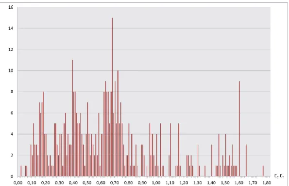
Since 1990s, a great deal of researches about deep level defects in SiC has been done with the help of DLTS or other investigation methods. The donor deep levels with almost full range of activation energy have been reported, as is shown in Figure 1.5. Obviously, these deep levels focus on activation energy from 0.1 eV to 0.9 eV, including the well-known Z1/2 defect with Ea around 0.68 eV.
Various of impurity defects have been investigated by means of doping or implanta-tion [44, 45], part of them found in 4H-SiC are illustrated in Table 1.4. Other impurity de-fects such as O and Er have been reported in 6H-SiC [46, 47].
Recently, more attention has been payed on characteristic of deep level defects and its relation to device properties. Danno and Kimoto have pointed out the similarity between Z1/2 and EH6/7 (with Ea around 1.6 eV) due to the fact that the concentration of Z1/2 and
1.2 Reliability and Defects
both centers contain the same defect such as a carbon vacancy [48]. As the two dominant electron traps, Z1/2 and EH6/7 could both survive after high temperature annealing at 1700 ℃ [49]. However, Klein argued that Z1/2 acted alone as the lifetime limiting defect [50]. By comparing the concentration of carbon vacancy (VC) determined by electron paramagnetic resonance with that of Z1/2 defect obtained by C-V and DLTS, Kawahara argued that the Z1/2 originates from VC [51], similar conclusion has been drawn in [52].
Figure 1.5. Number of articles which report defects with certain activation energy (ECET) in 4H-SiC.
Meanwhile, several effects have been put forward as
Poole-Frenkel Effect: The strong electric field close to the metal-semiconductor interface enhances the emission rate by lowering the potential barrier over which the carrier is thermally emitted. Therefore, increased applied electric field should lead to lower activation energy [53].
Carrier Freeze-out Effect: Strong compensation of the dopant and the high con-centration of radiation-induced defects takes place at low temperature [54]. Lambda Effect ( Effect): When measuring the deep levels in semiconductor
diodes, the transition zone near the edge of the space charge region (SCR) owing to the extended Debye tail of free carriers from the neutral material should be taken into consideration. Particularly, this width of correction should be fur-ther modified in non-steady state [55].
In addition, certain traps are invisible to the measurements that should be paid atten-tion as well. In particular, in the certain region near surface, electrons are not captured by the traps during the filling pulse. Whereas near the opposite edge of a depletion layer,
elec-trons in the deep level located below the Fermi level even when the reverse bias is applied can be always trapped without emission [56].
On the other hand, the correlation between the observation of the two barrier height behavior in the I-V characteristics and traps measured from DLTS and Random Telegraph Signal (RTS) dates back to year 2002 [57]. It was pointed out that the I-V characteristics tended to degrade with increasing deep-level concentration and those inhomogeneous di-odes tended to contain defect clusters, which can lead to a local Fermi-level pinning [18]. Gelczuk also argued that traps partially are responsible for the observed barrier height in-homogeneities [19].
Table 1.4. Several defects reported in 4H-SiC.
Defects EaECET (eV) 2 (cm ) NT (cm3) Reference Ti 0.13 7×10-15 3.66×10¹⁰ [45, 58, 59] 0.17 1×10-15 1.17×10¹¹ Cr 0.15 2×10-15 1.4×10¹³ [45, 58, 60-62] 0.18 8×10-16 1.3×10¹³ 0.74 2×10-15 \ V 0.80 1.79×10⁻¹⁶ 3×10¹⁷ [63] 0.89 \ < 1×10¹⁴ [62] 0.97 6×10-15 \ [45, 58, 59] Fe 0.39 2×10-15 7.6×10¹² [64] Ta 0.68 8×10-15 \ [65] Intrinsic 0.56 5×10-17 \ [56] 0.62 \ 1.2×10¹⁵ [49, 62] 0.66 1.31×10⁻¹⁴ \ [50, 66-68] 0.68 7×10-15 1×10¹³ [69-71] 0.72 2×10-14 9.5×10¹⁴ [48]
Chapter 2
Barrier height determination of
Schottky diodes
2.1 Energy band diagram and
formation of Schottky barrier diode
2.1.1 Ideal Schottky contact
Figure 2.1. Formation of an ideal Schottky barrier between a metal and an n-type semiconductor (a) neutral and isolated, (b) electrically connected by a wire, (c) separated by a narrow gap, (d) in perfect contact. Cross and circle marks in (b)
de-note donor ion and electron in conduction band respectively.
Consider an n-type semiconductor with a work function s less than that of the
met-al m, as shown in Figure 2.1(a). In this case, electrons will transfer from semiconductor to metal if they are connected by using a wire, and eventually the Fermi level in both metal and semiconductor would be consistent with uncompensated donor charge left near inter-face which leads to band bending and formation of a depletion layer as shown in Figure 2.1(b). Since the electron affinity of semiconductor s does not change, the difference of work function between metal and semiconductor falls on the voltage drop Vi between
them, as presented by Vi i if we assume the electric field i between two materials
be-2.1 Energy band diagram and formation of Schottky barrier diode
comes stronger with larger depletion region if the separation reduces which leads to re-duction on Vi, as illustrated in Figure 2.1(c). When they finally keep in touch [Figure
2.1(d)], the barrier owing to the vacuum no longer exists and it contributes to the ideal Schottky contact. In this case, the Schottky barrier height relates to the Fermi level is given by
B m
s
(2.1)In order to obtain Eq. (2.1) namely Schottky-Mott limit, a series of assumptions have been made:
The surface dipole contributions to m and s does not change or at least their difference does not change when the metal and semiconductor keep in touch. No localized states exist on the semiconductor surface.
The contact between the metal and semiconductor is perfect.
Similar analysis could be done with Schottky contact on p-type semiconductor where
m s
, while m s with n-type semiconductor or m s with p-type semiconduc-tor result in ohmic contact without rectifying effect. In this thesis we focus only on the n-type Schottky contact.
2.1.2 The effect of interface states
According to Eq. (2.1), the barrier height should directly depend on the metal work function m or in other words, the type of the metal. However, it has been experimentally found that the B is less sensitive to m as indicated by Eq. (2.1), and under certain cir-cumstances it could be almost independent of the metal type. This is because that the ideal situation illustrated in Figure 2.1(d) is never reached in real case. Even though the metal-semiconductor is well fabricated, a thin insulating film still exists at the interface due to the surface oxidation layer (~10 to 20 Å ) on the side of semiconductor, which results in the case more closed to that shown in Figure 2.1(c).
![Figure 1.1. Comparison of material properties of Si, SiC and GaN [3].](https://thumb-eu.123doks.com/thumbv2/123doknet/14529131.723295/32.892.266.631.773.1031/figure-comparison-material-properties-si-sic-gan.webp)
![Figure 1.4. Temperature dependence of forward I-V characteristics for 4H-SiC rec- rec-tifier reported in [19]](https://thumb-eu.123doks.com/thumbv2/123doknet/14529131.723295/36.892.227.643.188.494/figure-temperature-dependence-forward-characteristics-sic-tifier-reported.webp)
![Figure 2.6. The barrier height obtained from I-V measurements as a function of in- in-verse temperature in [86]](https://thumb-eu.123doks.com/thumbv2/123doknet/14529131.723295/62.892.260.631.451.805/figure-barrier-height-obtained-measurements-function-verse-temperature.webp)
![Figure 3.5. Difference in capacitance between two time points at various tempera- tempera-tures [113]](https://thumb-eu.123doks.com/thumbv2/123doknet/14529131.723295/73.892.169.728.255.665/figure-difference-capacitance-between-points-various-tempera-tempera.webp)
![Figure 3.8. Schematic illustration of pulse shape and capacitance transient in DDLTS [111]](https://thumb-eu.123doks.com/thumbv2/123doknet/14529131.723295/82.892.254.644.137.462/figure-schematic-illustration-pulse-shape-capacitance-transient-ddlts.webp)