Digital control of a stepping motor.
50
0
0
Texte intégral
Figure

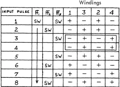
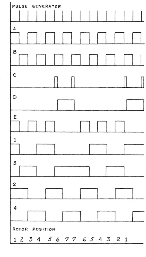
![Table 2.1 Step Sequence for Uniform PulsingFigure 2.31423Figure 2.4A -I -I- I I 8c F-]EJE1FC2 -4 -Posrri I I POSITION9](https://thumb-eu.123doks.com/thumbv2/123doknet/14746488.578375/16.940.285.696.182.515/table-step-sequence-uniform-pulsingfigure-figure-posrri-position.webp)
+5


Documents relatifs
