HAL Id: hal-03153799
https://hal.archives-ouvertes.fr/hal-03153799
Submitted on 26 Feb 2021HAL is a multi-disciplinary open access
archive for the deposit and dissemination of sci-entific research documents, whether they are pub-lished or not. The documents may come from teaching and research institutions in France or abroad, or from public or private research centers.
L’archive ouverte pluridisciplinaire HAL, est destinée au dépôt et à la diffusion de documents scientifiques de niveau recherche, publiés ou non, émanant des établissements d’enseignement et de recherche français ou étrangers, des laboratoires publics ou privés.
Ion Implantation as an Approach for Structural
Modifications and Functionalization of Ti 3 C 2 T x
MXenes
Hanna Pazniak, Mohamed Benchakar, Thomas Bilyk, Andrea Liedl, Yan
Busby, Céline Noël, Patrick Chartier, Simon Hurand, Marc Marteau, Laurent
Houssiau, et al.
To cite this version:
Hanna Pazniak, Mohamed Benchakar, Thomas Bilyk, Andrea Liedl, Yan Busby, et al.. Ion Implan-tation as an Approach for Structural Modifications and Functionalization of Ti 3 C 2 T x MXenes. ACS Nano, American Chemical Society, 2021, �10.1021/acsnano.0c06735�. �hal-03153799�
Ion Implantation as an Approach for Structural
Modifications and Functionalization of Ti3C2Tx
MXenes
Hanna Pazniak,*,† Mohamed Benchakar,‡ Thomas Bilyk,† Andrea Liedl,& Yan Busby,§ Céline Noël,£ Patrick Chartier,† Simon Hurand,† Marc Marteau,† Laurent Houssiau,/ Rosanna Larciprete,# Paolo Lacovig,// Daniel Lizzit,// Ezequiel Tosi,// Silvano Lizzit, // Jérôme Pacaud,†
Stéphane Célérier,‡ Vincent Mauchamp,*,† Marie-Laure David*,†
†Institute Pprime, UPR 3346 CNRS, Université de Poitiers, ISAE-ENSMA, BP 30179, 86962
Futuroscope-Chasseneuil Cedex, France
‡
Institut de Chimie des Milieux et Matériaux de Poitiers (IC2MP), Université de Poitiers, CNRS, F-86073 Poitiers, France
&INFN-LNF, P.O. box 13, 00044 Frascati (Rome), Italy
§Nanomatériaux pour les Systèmes Sous Sollicitations Extrêmes (NS3E), ISL-CNRS-UNISTRA
UMR 3208, French-German Research Institute of Saint-Louis, 68301 Saint-Louis, France
£IMEC, Kapeldreef 75, B-3001 Heverlee, Belgium
#CNR-Institute for Complex Systems (ISC), 00185 Rome, Italy
//Elettra-Sincrotrone Trieste S.C.p.A., AREA Science Park, S.S. 14 km 163.5, 34149 Trieste, Italy
E-mails: H.P. hanna.pazniak@univ-poitiers.fr; V.M. vincent.mauchamp@univ-poitiers.fr; M.-L.D. mldavid@univ-poitiers.fr
ABSTRACT: MXenes are a young family of two-dimensional transition metals carbides, nitrides, and carbonitrides with highly controllable structure, composition, and surface chemistry to adjust for target applications. Here, we demonstrate the modifications of two-dimensional MXenes by low-energy ion implantation, leading to the incorporation of Mn ions in Ti3C2Tx thin films.
Damages and structural defects caused by the implantation process are characterized at different depths by XPS on Ti2p core-level spectra, ToF-SIMS and with electron energy loss spectroscopy analyses. Results show that the ion-induced alteration of the damage tolerant Ti3C2Tx layer is due
to defects formation in both Ti and C sites, thereby promoting the functionalization of these sites with oxygen groups. This work contributes to the inspiring approach of tailoring 2D MXenes structure and properties through doping and defects formation by low-energy ion implantation to expand their practical applications.
KEYWORDS: Ti3C2Tx MXene, ion-implantation, defects, ToF-SIMS, XPS, TEM-EELS
MXenes, with structure Mn+1XnTx, where M stands for an early transition metal, X is C and/or N,
Tx is a surface termination and n = 1, 2, or 3, are single or few-layered two-dimensional (2D)
storage,2 sensing,3 catalysis,4 and optoelectronics.5 Thanks to the wide chemical and
stoichiometrical variability of parent MAX phases, where the A-group precursor elements usually belong to group 13 and 14 of the periodic table,6 MXenes can be easily adjusted to target
applications. With these possibilities, the MXenes exhibit high electrical conductivity,7
hydrophilicity,8 excellent mechanical properties,9 and technological flexibility.10-12 Among the
large variety of chemical compositions of MXenes that were experimentally13 and theoretically14
investigated, Ti3C2Tx is the first and the most intensively studied due to well-established synthesis
protocols providing high-quality and high yield 2D materials.15
To further extend MXenes applications, many attempts were made to modify their properties by applying different approaches and methods for surface chemistry engineering.16 A number of
reports were dedicated to effective etching protocols to modify the Ti3C2Tx surface.17-20 Depending
on the etching route, the selective etching of the MAX phase with fluoride and/or chloride-containing acid solutions, introduced different amounts of surface anion groups (=O, –OH, –F, – Cl), affecting the electronic density of states and other functional properties. Beyond allowing for the surface design, the etching protocol has also been adjusted to introduce defects in the MX core of the MXene sheets.21 Termination-engineering of Ti3C2Tx was also achieved by thermal
annealing in vacuum or in different gas media.22-24 In particular, the surface composition and the
electronic properties were controlled by the annealing temperature allowing for the de-functionalization of Ti3C2Tx.24 Several studies demonstrated the successful surface
functionalization of Ti3C2Tx with carboxyl,25 glycinegroups,26 and silane coupling agents,27,28
resulting in the improvement of the Ti3C2Tx stability25,27 and the charge percolation, which allowed
implementing the thin films in areas such as antibacterial coatings, fuel cells, surface-initiated polymerization, and absorbers.
Unfortunately, the multiple process variables such as the solution concentration, annealing temperature, etching duration, and media pH hinder the process reliability and reproducibility, resulting in a randomly distributed surface functionalization. The theory predicts that the bandgap and the magnetic properties could be engineered by adjusting the thin film chemistry and terminations.29 However, the lack of experimental verification confirms the practical difficulty of
such termination-engineering approach.
Introducing additional species into the layered MXene structure via ions intercalation is another strategy to control their properties.30 MXenes can be intercalated both chemically and
electrochemically by mono- and multivalent metal cations (such as H+, Li+, Na+, K+, Ca2+, Mg2+),
as well as by organic molecules.30-36 Cation-intercalated engineering allows controlling the
interlayer distance, which is directly proportional to the hydration size of the intercalated species, and to tune the mechanical and actuation properties of Ti3C2 MXene.35 This resulted in the
enhancement of the capacitance31,32,36 and sensing34 properties. However, since ions intercalation
mainly impacts the interlayer distance, it does not allow to deeply modify their physical properties. One of the recent chemical-based approaches to modify MXenes properties is the so-called “targeted etching”. It produces vacancy-ordered MXenes37,38 derived from in-plane ordered MAX
phase solid solutions by selectively etching both the A-element (Al) and the d-element on the M-position (for example Y or Sc). However, when the structure gets more complex, as for quarterly systems, a complete conversion of the MAX phase to a 2D structure becomes difficult.
Alternative strategies to tune MXenes properties include physical treatments with UV-ozone,39
electron beam irradiation,40 and plasma treatment.41 Nevertheless, even if these approaches have
Among the physical approaches used to infer specific characteristics to materials, ion-implantation has been widely used in the semiconductor industry as a powerful technique to modify the properties and structure of bulk materials through the controllable doping and damage formation.42
Whereas this technology is very mature in the silicon-based electronic device manufacturing, exciting applications have emerged such as in the solid-state quantum bits domain.43,44
Recently, ion-implantation was extended to atomically-thin 2D materials,45 such as graphene,46-54
transition metals dichalcogenides (TMDs, mostly MoS252,55 and WSe256) and hexagonal
boron-nitride.52 It was shown that low-energy ion implantation, with energy from several eV to tens of
keV, causes structural changes on 2D materials, which considerably impact the properties of materials due to the substitution of target atoms by doping ions and/or by the introduction of defects. So, doping graphene with ~1% 11B+ and 12C+ ions induces a strong negative
magnetoresistance at high magnetic field,46 while doping with nitrogen ions effectively raises the
position of the Fermi level thus affecting the graphene electronic properties. The incorporation of phosphorus ions in 2D TMDs enhances the photoluminescence, while in graphene it tunes the work function in a wide range (4.15-4.85 eV).57 The defects created by the ion-implantation in 2D
structures are a function of the implantation conditions and implanted ions species. At low fluence and energy below 100 eV, single vacancies,45,54 Stone-Wales defects45 and dangling bonds54 are
produced in single or few-layer 2D structures. At higher energy, structural disorder and amorphization are observed.45 It was successfully demonstrated that defect engineering in
graphene and 2D TMDs materials by ion-implantation allows tuning the electronic properties,49
the morphology and the stoichiometry of materials. The latter leads to unusual properties such as the metallic-like behavior of non-stoichiometric MoS254 and WSe2.56
In this paper, we carry out a systematic modification of Ti3C2Tx MXenes by ion-implantation with
manganese ions. This was motivated by recent theoretical predictions on the tuning of MXenes’ magnetic properties via strain, doping or defect engineering that attracted wide interest in the spintronics and quantum information communities.58 We find, that ion-implantation leads to
preferential Ti atoms sputtering with respect to the C atoms in the MXene layer. Such a sputtering offers new crystallographic sites available for the functionalization groups (oxygen) with a dramatic increase in the O content. The structural changes and damages introduced by the ion-implantation are investigated by spectroscopic studies, combining high resolution X-ray Photoelectron Spectroscopy (XPS) and Electron Energy-Loss Spectroscopy (EELS) in a Transmission Electron Microscope (TEM). The possibility of tuning the ion-implantation parameters in a wide range (nature and concentration of ion species, implantation energy) allows modifying and controlling the physical properties of MXenes.
RESULTS AND DISCUSSION
MXene film characterization
The Ti3C2Tx MXenes were synthesized using MILD59 (minimally intensive layer delamination)
conditions as described in the Materials and Methods section. The schematic structure and a typical transmission electron microscope (TEM) micrograph of delaminated Ti3C2Tx flakes
obtained from a colloidal solution are shown in Figure 1a-1b. The flakes are irregular in shape with an average lateral size of 2–10 µm. The flakes surface shows no visible defects, holes, nor impurities of the oxidized phase. The Selected Area Electron Diffraction (SAED) of the Ti3C2Tx
flakes (Figure 1b, inset) shows the hexagonal arrangements originating from the parent Ti3AlC2
Ti3C2Tx multi-layer films by spin-coating to achieve approximately a thickness of 100 nm. The
Scanning Electron Microscopy (SEM) image of the fabricated film (Figure 1c) shows that the Si/SiO2 substrate is fully and homogeneously covered since there are no naked regions over a
considerably large area. The cross-section SEM image (Figure 1c inset) reveals a compact film structure with well-resolved stacked layers aligned parallel to the Si/SiO2 substrate. The average
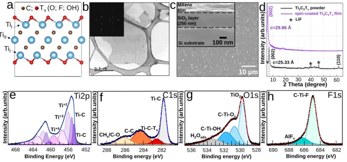
film thickness is about 100 nm with ~20 nm surface roughness associated with the spin-coating processing. The comparison between the X-Ray Diffraction (XRD) patterns of the as-prepared Ti3C2Tx powder and thin film (Figure 1d) shows that the film is characterized only by the sharp
and intense low angle (002) peak and the disappearance of the (110) peak confirming that film is well-aligned along the c-direction with the derived c-lattice parameter of 29.8 Å.
Figure 1. MXenes powder and thin film characterization. a) The schematic structure60 of
monolayer Ti3C2Tx MXene; TiI and TiII are surface and core Ti atoms, respectively, T is a surface
functional group; b) TEM micrograph of Ti3C2Tx flakes obtained from a delaminated colloidal
MXene solution with corresponding SAED pattern (inset); c) SEM image of MXene spin-coated thin film with a corresponding cross-section (inset) taken in Secondary Electron Imaging (SEI)
468 464 460 456 452
Binding Energy (eV) Ti-C Ti-C Ti+2 Ti+3 Ti+4 Ti2p 288 286 284 282
Binding energy (eV)
C1s Ti-C Ti-C-Tx C-C CHx/C-O
d
c
e
f
536 534 532 530 528Binding energy (eV)
O1s C-Ti-Ox C-Ti-OH H2Oads TiO2
g
690 688 686 684 682 F1sh
Binding energy (eV) C-Ti-F AlFx 100 nm MXene film SiO2layer (250 nm) Si substrate 10 2 Theta (degree) 20 30 40 50 60 Inte n s it y (a rb.un it s
) spin-coated Ti3C2Tx filmTi3C2Txpowder
c=25.33 Å c=29.86 Å (00 2 ) 10 µm Inte n s it y (a rb.un it s ) Inte n s it y (a rb.un it s ) Inte n s it y (a rb.un it s ) Inte n s it y (a rb.un it s )
a
TiI TiII TiI Tx (O; F; OH)b
C; (1 1 0 ) * * * LiF (00 2 )mode; d) XRD patterns of the as-synthesized Ti3C2Tx powder and spin-coated thin film; e), f), g),
h) High-Resolution (HR) core-level spectra of Ti2p, C1s, O1s, and F1s from a spin-coated MXene film.
The HR-XPS spectra from the freshly deposited Ti3C2Tx thin film are shown in Figures 1e-1h. For
the Ti2p spectrum the main doublets related to the MXene structure have the 3/2 spin orbit component at 454.8, 455.2, 456.0, 457.4 eV,61 whereas the minor peak, appearing at 459.3 eV
(Ti+4) is attributed to the formation of a small amount of oxidized TiO2 phase. Both Ti2p peaks at
454.8 and 455.2 eV are attributed to Ti-C bonds in the MXene structure, being the peak at higher binding energy related to the presence of neighboring lattice defects.61
The peaks located at 456.0 and 457.4 eV are attributed to Ti+2 and Ti+3 and correspond to titanium
atoms bonded with carbon and functional groups C–Ti–O, C–Ti–F,20 and C–Ti–OH.61 For the C1s
spectrum, the main peak, related to the Ti–C bonds appears at 281.8 eV and the second one attributed to Ti–C–Tx appears at higher energy (282.5 eV). The two minor peaks, at 284.3 and
286.2 eV are assigned to graphitic C–C bonds and organic CHx/C–O contaminations. The O1s
spectrum shows three peaks at 529.6, 530.7, and 531.7 eV attributed to the functionalized C–Ti– Ox and C–Ti–OH phases, respectively.62 The fourth minor component at 533.4 eV is related to
adsorbed H2O. The F1s spectrum shows a strong component at 685.0 eV attributed to the C–Ti–
Fx bonds arising from the MXene surface functionalized by fluorine groups and a weak shoulder
fingerprint of AlFx at 686.3 eV.61
Ion implantation of Ti3C2Tx thin films
The 100 nm-thick Ti3C2Tx films were directly exposed to the ion beam as detailed in Materials
and Methods. For many 2D materials such as MoS263 or graphene, because of growing limitations,
damages, the doping of few-layers 2D materials was performed at low beam energy (25 eV – 2 keV) or by depositing an additional protection layer57,64 on the top of the 2D material. In our
case, the 100 nm thick multi-layer MXenes film allows using a higher energy beam (tens of keV) to implant the whole film with Mn ions. The 55Mn+ implantation is performed at 60 keV at fluences
of 1·1015 and 1·1016 ions/cm2 to generate specific ion distribution/damage profiles with projectile
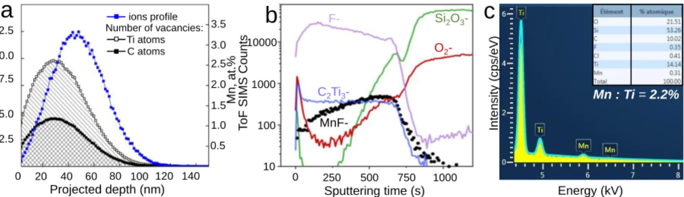
depths compatible with the thickness of the MXene film, according to Stopping and Range of Ions in Matter (SRIM) simulations shown in Figure 2a.
Figure 2. (a) The SRIM simulated depth profiles of Ti and C atoms vacancies (black curves) and
55Mn+ ion distribution (blue curve) within the Ti
3C2Tx thin film following the ion-implantation
with 1·1016 ions/cm2 fluence at 60 keV energy. The Ti and C vacancy profiles are given for a
qualitative estimation; (b) ToF-SIMS depth profiles of 55Mn+-implanted Ti3C2Tx thin films at 60
keV with 1·1016 ions/cm2 fluence; (c) EDS spectrum of Ti3C2Tx thin film implanted with 1·1016
Mn-ions/cm2 at 60 keV.
Based on SRIM calculations, for 60 keV energy of Mn+ ions, the projected range and the average
straggling are equal to 47.7 and 20.3 nm respectively. Thus, the Mn-ions distribution is Gaussian-like and the maximum should occur in the middle of the Ti3C2Tx film (Figure 2a). The simulated
damage profile (numbers of vacancies on Ti and C atoms) is more asymmetric than ions profile and reveals that the near-surface region of the film might be highly damaged. The tail of the
a
b
10 23 vaca nci es/cm 3 Mn, at .% 20 40 60 80 100 120 140 0 Projected depth (nm) 2.5 5.0 7.5 10.0 12.5 0.5 T oF SIM S Coun ts 0 250 500 750 1000 Sputtering time (s) MnF-C2Ti3 -O2 -Mn : Ti = 2.2% Energy (kV) F- Si2O3 -10 100 1000 10000 1.0 1.5 2.0 2.5 3.0 3.5 Number of vacancies: ions profile Ti atoms C atomsc
Int ensi ty (cps/ eV)damage distribution is observed close to the Si/SiO2 substrate which means that in this region the
film should be less damaged. Moreover, the SRIM calculations gives the value of the sputtering yield, Y, defined as an average number of atoms leaving the surface of a solid per incident particle. The sputtering yield of Ti atoms from the simulated structure of Ti3C2 is 0.22 atoms/ion, whereas
the sputtering yield of C atoms is 0.07 atoms/ions. Since the SRIM code applies to bulk materials, as an approach to simulate the implantation profile, we have considered the Ti3C2 density of 3.20
g/cm3 as the average density of the multilayer stacked thin film, which might be overestimated.
Thus, we account for the SRIM results only from a qualitative point of view, suggesting the preferential sputtering of Ti atoms as compared with C atoms during Mn implantation.
It is difficult to directly translate SRIM results to the real ion distribution in the MXenes film since bulk materials with homogeneous density and exact chemistry are sensibly different from atomically-thin single- and multilayer stacked 2D materials. To obtain experimental evidence of the Mn profile in the Ti3C2Tx film and correlate these results with SRIM calculations, we
performed Time-of-Flight Secondary Ion Mass-Spectroscopy (ToF-SIMS) (Figure 2b) on ion-implanted films. The ion-implanted samples were sputtered with low-energy (0.5 keV) Cs+ beam and
analyzed with a short impulse of Bi3+ beam at 25 keV. Cesium sputtering was chosen because it is
a universal sputtering source for organic and inorganic materials which does not introduce major artifacts (no preferential sputtering or reduction of metals nor accumulation of in depth-modifications) and will not significantly modify the chemical composition of the exposed sample surface. The ToF-SIMS depth profile analysis clearly shows that the Mn distribution, assessed by the MnF- ion, is uniform in the log plane and it increases monotonically along with the depth
(sputtering time) of the Ti3C2 film which shows a stable intensity as monitored by the C2Ti3- ion.
with other ions. The maximum of the Mn concentration is found close to the SiO2 substrate which
is identified by the rise of Si2O3- and O2- signals. We also observe a raise of the Si2O3- signal at the
beginning of the profile which is a frequently observed feature ascribed to surface contamination by polydimethylsiloxane. The discrepancy between the ToF-SIMS and SRIM profiles is possibly explained by (i) the 2D nature of Van der Waals bonding between MXene sheets, (ii) the roughness of the film or (iii) the Cs+ sputtering-related artifacts.65,66 Despite this, the experiment confirms
that the Mn doping is successfully achieved in the fabricated thin film as proved by the bulk-sensitive Energy-dispersive X-ray Spectroscopy (EDS) analysis (Figures 2c), indicating ~2.2 at.% Mn doping which is lower as compared with the value at the maximum of the SRIM profile.
Spectroscopic characterization of implanted Ti3C2Tx thin films
To follow the structural damages and chemical modifications induced in the Ti3C2Tx film surface
by the Mn-ions implantation we perform high-resolution XPS depth profiling (Figure 3) and EELS analysis (Figures 4-5).
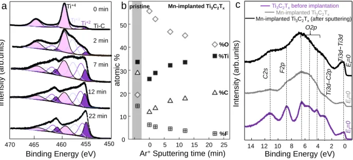
In the former case the sample was sputtered with low-energy (500 eV) Ar+ beam which, as well as
Cs sputtering in ToF-SIMS, allows limiting in-depth damages for 2, 7, 12 and 22 min and the Ti2p spectra measured at increasing depths are shown in Figure 3a together with the results of the best-fitting analysis. In agreement with Figure 1e, four spectral components are identified, labeled as Ti–C (from the MXene structure at ~455.2 eV binding energy), Ti+2, Ti+3 and Ti+4 (from oxidized
TiO2 phase, at ~459.5 eV). After implantation, the Ti2p spectrum looks very different from the
pristine film (Figure 1e); we observe a very intense contribution from the oxide phase, in particular, the Ti+4 doublet which dominates the spectrum. After 22 min of Ar+ sputtering, the oxidized layer
is partially removed and the Ti2p spectrum is peaked at ~ 455.5 eV and starts to resemble that of freshly deposited Ti3C2Tx film (see Figure 1e). The rather long sputtering time required to partially
decrease the oxidized phase testifies that the chemical modification induced by the implantation extends well below the film surface (7-8 nm from the surface).
Figure 3. a) Ti2p HR-XPS spectra of Mn+-implanted Ti3C2Tx thin film (1·1015 ions/cm2 at 60 keV)
after sputtering at different times; b) Evolution of the film composition (O, Ti, C, and F atomic %) with the sputtering time (500 eV Ar+) as derived from the analysis of survey spectra for the
Mn-implanted film as compared to the pristine Ti3C2Tx film (before implantation); c) Valence band
XPS spectra of pristine Ti3C2Tx thin film, after implantation with 1·1015 ions/cm2 at 60 keV, and
after 22 min Ar+ ion beam etching.
However, the XPS measurements point out that both the Ti3C2Tx film chemical composition in the
surface and its depth are modified by the Mn-ions implantation; in particular, the oxygen content (Figure 3b) and Ti3+ component are still higher as compared to the pristine film (Figure 1e). This
suggests that the Ti–C bonds dissociated by the impinging Mn-ions quickly react with oxidizing species present in the background pressure inside the implanter or, more effectively, with atmospheric water and oxygen adsorbates when the reactive Ti3C2Tx surface is extracted from the
implanter. The formation of an oxidized phase on the top of the implanted surface was also
Int en si ty (a rb .un its )
Mn-implanted Ti3C2Tx(after sputtering)
a Int en si ty (a rb .un its ) 470 465 460 455 450
Binding Energy (eV) 22 min 12 min 7 min 2 min 0 min Ti-C Ti+2 Ti+3 Ti+4 0 5 10 15 20 25
Ar+Sputtering time (min)
0 10 20 30 40 50 a tomi c % Mn-implanted Ti3C2Tx %O %Ti %C %F b Ti3C2Txbefore implantation Mn-implanted Ti3C2Tx 0 2 4 6 8 10 12 14
Binding Energy (eV)
Ef =0 c Ef =0 Ef =0 T i3 d− T i3 d T i3 d – C2p C2s O2p F2p pristine
observed after ion-irradiation of 2D MoS2 with swift heavy ions resulting in production of active
low-coordinated Mo atoms.67,68 The observed increase in the Ti-Ox and Ti-OH bonds (Ti3+
component) more in depth agrees with the decaying O2- profile in the ToF-SIMS measurements
during the 300 s of Cs+ sputtering (Figure 2b) which is well above the time necessary to typically
remove oxidized surface contaminating layers (i.e. few seconds).
From the survey XPS spectra measured at 1030 eV (Supporting Information, Figure S1) we have calculated the sample composition as a function of the sputtering time (Figure 3b). The slight higher amount of C found in pristine MXene film as compared with stoichiometric value is ascribed to the surface contamination. From the evolution of the chemical composition with the Ar+ sputtering time, we can follow the non-stoichiometric ratio between Ti and C atoms. Namely,
while both %Ti and %C increase with the sputtering time (t), the Ti/C ratio decreases from 2.1 (t=0 min) to 1.8 (t=22 min) thus slowly approaching the nominal value of 1.5 (Ti3C2).
Simultaneously, the fluorine and oxygen content decreases. However, even after t=22 min, the amount of oxygen is still two times higher than in the pristine film, indicating that defective sites are still occupied by oxygen atoms mainly forming Ti+3 state.
From the valence band of Ti3C2Tx films (Figure 3c) we immediately see that the electronic
structure is modified by ion implantation; the main Ti3d-C2p, O2p, and F2p69 bands are strongly
broadened and can hardly be resolved after Mn-ion implantation and after Ar+ ion beam sputtering.
This indicates a structural disorder in the Mn-implanted MXene structure. Nevertheless, the valence band maximum is still at the Fermi level (Ef), confirming that the implanted MXene film
is still metallic with Ti3d states at Ef. We conclude that, despite the structural damages due to the
1 1015 Mn/cm2 implantation and induced increase of O content, the MXene maintains its metallic
Next, TEM-EELS are performed to better understand damages induced by ion-implantation. Electron spectroscopy has been demonstrated as powerful tool for the investigation of radiation-induced damages at the local scale in various materials including MAX phases and graphite.70,71
The changes in the fine structure or an energy shift is an indication of different chemical compositions and/or crystallographic structure modification.72
In order to get a complementary picture of the films, especially the region with the higher Mn amount, TEM-EELS has been performed on very thick parts extracted from the two spin-coated films implanted at 1 1015 and 1 1016 ions/cm². The thicknesses of the two regions were similar and
correspond to the thickness to inelastic mean free path ratio of 0.65 to 0.7. (Figure 4).
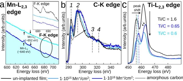
By recording EEL spectra at the Mn-L2,3 edges in the implanted films (Figure 4a), we observed
that the sample implanted at 1·1015 ions/cm2 shows almost negligible Mn-L3 line; this very low
doping reasonably agrees with SRIM calculations predicting the Mn concentration of ~0.32 at.% (Supporting Information, Figure S2). On the other hand, a more defined and sharper Mn-L3 line is
obtained when the implantation fluence is raised to 1·1016 ions/cm2. However, the intensities of
Mn-L2,3 lines of Ti3C2Tx films at both fluences are weak and detailed information about the Mn
chemical environment difficult to extract. The F-Kedge signal in the investigated zones is rather low as compared with pristine un-implanted film (Figure 4a, inset).
Figure 4. Mn-L2,3 (a), C-K (b), and Ti-L2,3 edges (c) EEL spectra of Ti3C2Tx films before and after
Mn-implantation at 60 keV with 1·1015 and 1·1016 ions/cm2 fluence. C-K edge EELS spectrum of
amorphous carbon is recorded as the reference.
In order to characterize the Ti-C bonding of the Ti3C2Tx structure after implantation at 1·1015 and
1·1016 ions/cm2 fluences, we compare the EEL spectra at C-K and Ti-L2,3 edges in implanted and
un-implanted films (Figure 4b-4c). Amorphous carbon is also recorded for reference. The C-K edge EELS signal from pristine Ti3C2Tx film shows the presence of four peaks which are typical
for Ti3C2Tx structure.73 These peaks are still intense and well-resolved after implantation, however,
according to the fluence, we observe a progressive decrease of peak 1 and a broadening of peaks 2, 3, and 4. In agreement with the lower fluence, the broadening of peak 2 in the C-K edge EELS spectrum for the sample implanted with 1 1015 ions/cm² is lower than that for the 1 1016 ions/cm²
sample. The broadening testifies a higher structural disorder, which has been commonly observed in carbon-based materials when structural distortions take place.71 These results confirm the
fluence-dependent structural distortion in Ti–C layers after implantation and reveals that the amount of damage is being controllable over one or two orders of magnitude by tuning the fluence.
1·1015 Mn+/cm2; 1·1016 Mn+/cm2; amorphous carbon. un-implanted film;
c
a
Inten sity (arb .un its) 600 620 640 660 680 700Energy loss (eV)
Mn-L3 (~640 eV) Mn-L2 (~652 eV) F-K edge pristine Ti3C2Tx
Mn-L
2,3edge
Inten sity (arb .un its) 280 300 320 340Energy loss (eV)
C-K edge
1 2
3 4
b
Inten sity (arb .un its) 460 450 470 480Energy loss (eV)
Ti-L
2,3edge
peak shift Ti/C = 0.65 Ti/C = 0.6 Ti/C = 1.6 F-K edge F-K edge 680 690Very important, neither for the 1 1015 nor 1 1016 ions/cm2 fluences the structural disorder leads to
the amorphization of the MXene as testified by SAED patterns given in Figure S3 where no amorphization ring is observed. Under implantation conditions, the MXene flakes are thus damage tolerant allowing to use ion implantation to induce structural modification.
By normalizing spectra at the C-K edge, we can visualize the induced modifications at the Ti-L edge (Figure 4c). In particular, the drop in the intensity of the Ti-L2,3 double peak (at 456 and 462
eV) indicates preferential sputtering of Ti atoms with respect to carbon atoms. The presence of titanium surface atoms (TiI) exhibiting smaller bounding energy than the bulk ones (TiII) in
Ti3C2Tx structure (Figure 1a) and the larger cross section of Ti atoms for elastic collisions
involving Mn-ions as compared with C atoms dictates that defect production involving Ti atoms are statistically more probable.
Moreover, the energy shift of the Ti-L2,3 lines (+0.6 and +1.6 eV depending on the fluence)
indicates the progressive increase of Ti oxidation state72 (Figure 3a). Having a closer look at the
Ti-L2,3 edge EELS spectrum for the sample implanted with 1 1016 ions/cm², we notice that the
lines are slightly asymmetric. However, the Ti-L2,3 edge is clearly different from highly oxidized
Ti3C2Tx MXene where the asymmetry of four peaks is well-resolved (Supporting Information,
Figure S4). The diffraction spots corresponding to tetragonal anatase phase of TiO2 presented in
SAED patterns of implanted MXenes (Supporting Information, Figure S3) originate from the oxidation of the top surface film layers. Since the EELS signal integrates information from the whole film thickness, the signal from distorted surface layers characterized by stronger oxidation is superimposed to the one from the underlying preserved film. Overall, the analysis of C-K and Ti-L2,3 edges points out that ion-implantation induced damages on both C and Ti atoms without
Based on the spectroscopic study provided on the implanted Ti3C2Tx thick films we can conclude
that ion implantation results in successful Mn incorporation with partial damaging of the Ti3C2Tx
crystal structure. The last is confirmed by the gradual drop of (002) peak intensity in XRD patterns (Supporting Information, Figure S5). The additional peaks on the implanted sample in Figure S5 are due to the SiO2 substrate. This confirms the sputtering of Ti and C atoms in the near-surface
layers induced by the ion-implantation.
Since the Mn concentration is negligible when the fluence of 1·1015 ions/cm2 is used, we further
explored film implanted with 1·1016 ions/cm2. To get precise information about damages occurring
in MXenes flakes upon implantation excluding surface oxidation effect, we detached the film from the substrate, put different parts of the film in ultra-high purity water and drop it on carbon-supported membrane. We analyze only buried sheets with EELS picking the signals from three different regions (R1-R3) (see Supporting Information, Figure S6, for detailed description), each of which may be related to a different implantation depth. The ratio between the film thickness and the inelastic mean free path (1/lambda) in R1, R2, and R3 are 0.40, 0.20 and 0.21 respectively, meaning that we analyze regions with different thicknesses. The results are shown in Figure 5 and corresponding SAED patterns of studied regions are in Supporting Information, Figure S7.
Int ens ity (a rb .unit s)
c
d
R3 R2; R1; de crea se in ten sity spu tt eri ng Ti-L2,3edgea
280 300 320 Int ens ity (a rb .unit s)Energy loss (eV)
b
340 C-K edge 1 2 3 4 450 460 470 480 490 Energy loss (eV)0.3 0.6 0.9 1.2 1.5 Mn-implanted Ti3C2Tx pristine R1 R2 R3 O/Ti Ti/C O-K edge 1 2 3 520 530 540 550 560 570 Energy loss (eV)
Int ens ity (a rb .unit s) Ra tio 1.8
Figure 5. C-K (a), Ti-L2,3 (b), and O-K (d) edges EEL spectra of different regions from Ti3C2Tx
films after Mn-implantation at 60 keV with 1·1016 ions/cm2. The O-K edge spectra were
normalized on the first peak intensity. The Ti-L2,3 edges are normalized to the C-K edge in (a). (c)
The Ti/C and O/Ti composition ratio of different regions of Mn-implanted Ti3C2Tx film as derived
from elemental quantification of EELS spectra as compared to the pristine Ti3C2Tx film (before
implantation).
With respect to the pristine film spectrum, the C-K edge region (Figure 5a) features different degrees of distortions, going from barely almost un-modified peaks (in R1) to the 20-25% reduction of the peak 1 and comparable broadening of peak 2 (in R2 and R3). It is worth noticing that the peak 2 broadening is considerably lower respect to the one recorded in amorphous carbon (Figure 4a), evidencing a high damage tolerance of the Ti3C2 layer. According to the modeled
SRIM profile, the less damaged structure should be in the middle of the film and close to the substrate.
From the Ti-L2,3 edge spectra analysis we conclude that the R3 region, showing the highest
broadening of C-K edge, is also the one showing the strongest drop of the Ti-L2,3 peaks intensities
(Figure 5b) and maximum sputtering yield of Ti atoms with respect to C atoms. The Ti content with respect to C is significantly reduced as compared to the pristine sample (Figure 5c). However, both damaged regions R2 and R3 do not show any shifting of the position of the peaks (Figure 5b) nor the presence of additional phases in SAED (Figure S7), confirming that oxidation is limited only to the more exposed top-surface sheets.
By analyzing the O-K edge (Figure 5d), we observe that EELS signal from implanted Ti3C2Tx
regions R1 and R2 shows the presence of three peaks similar to O-K edge usually observed in Ti3C2.73 The O content (O/Ti) is gradually increased from R1 to R3 and correlates with Ti
sputtering (Ti/C) as evidence by EELS quantifications (Figure 5c). The R3 region, showing the maximum sputtering yield of Ti atoms, is also the one showing the highest O content. As can been seen, the O/Ti ratio in R3 region is about 1.5 and this value is twice that of the pristine un-implanted sample. This finding evidences the fact that Ti sputtering promotes new crystallographic sites, occupied by O atoms. This result is further confirmed by a strong modification of the O-K edge fine structure with a much more intense peak 2 (at ~ 538 eV) as compared with R1 and R2 regions indicating considerable changes in the local environment of the oxygen atoms (Figure 5d). A similar O-K edge EELS signal was experimentally recorded at graphene oxide.74 This suggests
that the extended zones of the MXene sheets surfaces where Ti has been preferentially sputtered offer new cites for oxygen bonding with the carbon planes, leading to a significant amount of oxygen atoms experiencing a G-O-like environment. This is in agreement with the SAED collected on region R3 (see Figure S7c) where additional rings, consistent with the GO structure, are also observed. These results are in agreement with Ti3C2 oxidation experiments reported recently and
showing that Ti-vacancies promote the nucleation and oxidation of amorphous carbon clusters.75
Moreover, ab initio molecular dynamics simulations21 have shown that water molecules and
oxygen adsorbates are preferentially located close to Ti vacancies. It could thus result in the formation of the graphene oxide structure at the local level as experimentally evidenced by TEM and EELS (Figure 5d, Figure S7c). The presence of peak 1 (Figure 5d), not ascribed to C-O like bonding, confirms that some of the original oxygen sites are preserved while the new ones are promoted. We can safely exclude that this feature is related to the formation of titanium dioxide in the sub-surface layers since the O-K edge spectrum of oxidized Ti3C2Tx looks completely different
As a major result, thanks to the damage tolerance of the Ti3C2 sheets to ion implantation, this
approach can be used to generate a high amount of both Ti and C extended defects, promoting oxygen functionalization as shown here using XPS and TEM-EELS. We conclude that the disordered character of the Ti3C2Tx induced by ion-implantation is extremely favorable for the
spontaneous functionalization of defective titanium and carbon sites with oxygen.
CONCLUSIONS
In this work we investigate ion-implantation of Ti3C2Tx MXene thin films. The presence of Mn
ions implanted at 60 keV was confirmed by ToF-SIMS depth profiling, EDS, and EELS analyses. Interestingly, the ion-implantation introduces a Mn doping profile and complex structural changes in stacked 2D MXenes while keeping their metal-like behavior. The XPS analysis evidenced that ion-implantation causes oxidation of the top-surface sheets due to the harsh sputtering of titanium and carbon atoms resulting in the formation of a large number of dangling bonds and reactive surface defects. The EELS proved the structural distortion gradient decay through the depth of Ti3C2Tx film characterized by different degrees of defects formation in both Ti and C sites while
keeping the original MXene structure suggesting their damage tolerance to ion-implantation. The disorder induced in ion-implanted Ti3C2Tx is found to be extremely favorable for the
functionalization of defective titanium and carbon with oxygen functional groups, thereby increasing the amount of oxygen in MXene flakes and modifying their electronic structure. We believe this strategy is perspective and could be extended to other MXenes since oxygen functionalization is predicted to tune a band gap in different MXenes chemistry.
Since defects have been widely demonstrated to effectively tailor the carrier types and optical response in many 2D materials, ion implantation appears a practical, controllable and
easily-implementable tool to modify the electronic properties of MXenes. Defects are also beneficial for a number of applications such as photocatalysis, catalysis, micro-wave absorption and pseudocapacitance. The ion-implantation approach offers a great variety of adjusting parameters such as the dopant type, fluence and energy which can be selected to meet specific applications of MXenes in a wide range of research fields.
EXPERIMENTAL SECTION
MXenes synthesis and thin film preparation. The Ti3C2Tx MXenes were synthesized from
Ti3AlC2 precursor using the MILD(minimally intensive layer delamination) conditions, which
means exfoliation of 0.5 g of Ti3AlC2 (initial particles sizes < 25 µm) at 40 °C in 10 ml solution of
0.8 g LiF dissolved in 9M HCl under continuous magnetic stirring during 24 h. The suspension obtained after etching, including Ti3C2Tx and non-reacted Ti3AlC2,was centrifuged 8 times at 6000
rpm for 6 min and the supernatant liquid was systematically removed. The black Ti3C2Tx slurry
was then carefully collected and separated from the surface of the sediment Ti3C2Tx/Ti3AlC2 with
a spatula. The slurry was then filtered, washed and dried one night under air at room temperature and finally stored under inert atmosphere. This synthesis method is partly based on the work of Alhabeb et al.15
The Ti3C2Tx thin films were produced by spin coating of delaminated concentrated Ti3C2Tx
colloidal solution (concentration is ~ 70 mg/ml), obtained by simply manual shaking of a water suspension of multilayer MXenes as produced above, onto a Si substrate with 250-nm-thick SiO2
(1x1) cm2 area. Before deposition, the substrates were cleaned by sonicating in acetone in an
were deposited using Polos SPIN150i/200i spin coater at room temperature in a multistep regime to achieve 100 nm thickness and dried overnight under vacuum conditions.
Ion-implantation. We prepared eight spin-coated Ti3C2Tx films for one implantation since we
used destructive techniques to characterize samples after implantation (XPS depth profile and ToF-SIMS). All samples were mounted on a cooled sample holder and directly exposed to the ion beam having an implantation surface of about 25 cm2. Thin films were prepared before implantation to
avoid contamination problems. 55Mn+ ions of 1·1015 and 1·1016 ions/cm2 were accelerated at 60
keV with probe currents of 2.1-7.0 µA and a chamber pressure of ∼5×10⁻⁷ mbar at room
temperature. The projectile trajectory of implanted ions was perpendicular to the surface of thin films. The damage and ion distribution depth profiles of Ti3C2Tx thin film (density of 3.20 g/cm3)
were simulated using the Stopping and Range of Ions in Matter (SRIM) code.76 The displacement
energies used were Ed = 25 eV for Ti and Ed = 28 eV for C. The number of created vacancies were
calculated using the detailed calculation with full damage cascades method.
Ti3C2Tx thin film characterization. The X-Ray diffraction (XRD) patterns of the Ti3C2Tx
powder, spin-coated Ti3C2Tx thin films before and after ion-implantation were collected at room
temperature using D8 Diffractometer (Bruker Ltd. Germany) with a continuous θ–2θ scan with 0.017 ° 2θ/sec and Cu-Kα radiation (1.5406 Å) at U = 40 kV, I = 40 mA. Thin films’ morphology and chemical composition were studied using JSM-7001F TTLS field emission gun scanning electron microscope (Jeol Ltd., Japan) equipped with an Energy Dispersive X-ray Spectrometer (EDS) from Oxford Instruments (UK).
The TEM samples were prepared by detaching the Ti3C2Tx implanted film from the substrate by
lightly brushing with a soft sharpened stick, put different fragments of the film in ultra-high purity water to avoid further agglomeration and drop it on Cu grid covered with a lacey carbon film. The
MXene films of different thicknesses were probed with the electron beam normal to the film. The Electron Energy Loss Spectroscopy (EELS) spectra were recorded in image mode in a JEOL 2200 FS microscope equipped with an in-column omega filter and operated at 200 kV. The energy resolution determined from the loss peak full width at half maximum was 1.0 eV. The zero-loss peak was used to align in the energy scale the signal of the C-K edge, Ti-L2,3 edge, and O-K
edge spectra. The core edges were extracted from the background signal using a power law and were deconvolved from multiple scattering using the Fourier-ratio method. The acquisition conditions were optimized for each edge to avoid irradiation damages.
High-resolution (HR) core-level photoemission spectroscopy (XPS) was performed at the SuperESCA beamline of the Elettra synchrotron radiation facility (Trieste, Italy). Survey and HR core-level and valence band spectra of Ti3C2Tx thin films were collected at a photon energy of
1030 eV and 100 eV respectively. For each spectrum, the binding energy was calibrated by measuring the Fermi level of the gold foil in contact with the sample. Core levels spectra were best-fitted with Voigt functions after Shirley background subtraction. The implanted MXenes thin films were repeatedly sputtered with 0.5 keV Ar+ at 5·10-6 mbar with the ion beam hitting the
sample at 20 ° to normal. After each sputtering cycle survey and HR Ti 2p spectra were recorded at photon energy of 1030 eV.
Time-of-Flight Secondary Ion Mass-Spectroscopy (ToF-SIMS) depth profiles were acquired using a dual-beam ToF-SIMS IV spectrometer from ION-TOF GmbH (Münster, Germany) in non-interlaced mode, alternating 1-frame analysis with Bi3+ (energy 25 keV at the ion current of ~0.2 pA, analysis area of 100×100 μm2) and 10 s of sputtering with 500 eV Cs+ (at an ion current of
on, the sample surface was flooded using a defocused low-energy electron beam to sustain surface charge compensation.
ASSOCIATED CONTENT
Supporting Information. The Supporting Information is available free of charge on the ACS
Publications website. Additional information about the survey spectra of Ti3C2Tx film, SRIM
simulated profile of implanted film, XRD patterns, TEM micrographs, and SAED patterns of implanted Ti3C2Tx films, Ti-L2,3 (b), and O-K edge EEL spectra of oxidized Ti3C2Tx flakes, and
schematic description of Ti3C2Tx ion implantation procedure and the implanted film “structure”.
AUTHOR INFORMATION
Corresponding Authors
*Emails: hanna.pazniak@univ-poitiers.fr (H.P.); vincent.mauchamp@univ-poitiers.fr (V.M.);
mldavid@univ-poitiers.fr (M.-L.D.)
Notes
The authors declare no competing financial interest. ACKNOWLEDGMENT
This work was partially funded by the “Région Nouvelle-Aquitaine” and the European Regional Development Fund (ERDF 2014-2020) within the NanoTrans project No. PC-2016-2916910. H.P. and R.L. thanks the Elettra Synchrotron Facility (proposal №20190484). The research leading to this result has been supported by the project CALIPSOplus under Grant Agreement 730872 from the EU Framework Programme for Research and Innovation HORIZON 2020. The authors also
acknowledge financial support from the French research ministry (Ph.D. thesis of M.B.) and “Agence National de la Recherche” (reference ANR-18-CE08-014 – MXENECAT project). REFERENCES
1. Naguib, M.; Kurtoglu, M.; Presser, V.; Lu, J.; Niu, J.; Heon, M.; Hultman, L.; Gogotsi, Y.; Barsoum, M.W. Two-Dimensional Nanocrystals Produced by Exfoliation of Ti3AlC2. Adv. Mater.
2011, 23, 4248–4253.
2. Anasori, B.; Lukatskaya, M.; Gogotsi, Y. 2D Metal Carbides and Nitrides (MXenes) for Energy Storage. Nat. Rev. Mater. 2017, 2, 16098.
3. Kim, S.-J.; Koh, H.-J.; Ren, C. E.; Kwon, O.; Maleski, K.; Cho, S.-Y.; Anasori, B.; Kim, C.-K.; Choi, Y.-K.; Kim, J. Gogotsi, Y.; Jung, H.-T. Metallic Ti3C2Tx MXene Gas Sensors with Ultrahigh
Signal-to-Noise Ratio. ACS Nano 2018, 12, 986–993.
4. Li, Z.; Wu, Y. 2D Early Transition Metal Carbides (MXenes) for Catalysis. Small 2019, 15. 1804736.
5. Hantanasirisakul, M.; Lipatov, A.; Maleski, K.; Anasori, B.; Salles, P.; Ieosakulrat, C.; Pakawatpanurut, P.; Sinitskii, A.; May, S.J.; Gogotsi, Y. Effects of Synthesis and Processing on Optoelectronic Properties of Titanium Carbonitride MXene. Chem. Mater. 2019, 31, 2941–2951. 6. Sokol, M.; Natu, V.; Kota, S.; Barsoum, M. W. On the Chemical Diversity of the MAX Phases. Trends Chem. 2019, 1, 210–223.
7. Hang, J.; Kong, N.; Uzun, S.; Levitt, A.; Seyedin, S.; Lynch, P. A.; Qin, S.; Han, M.; Yang, W.; Liu, J.; Wang, X.; Gogotsi, Y.; Razal, J. M. Scalable Manufacturing of Free‐Standing, Strong Ti3C2Tx MXene Films with Outstanding Conductivity. Adv. Mater. 2020, 32, 2001093.
8. Huang, S.; Mochalin, V. N. Hydrolysis of 2D Transition-Metal Carbides (MXenes) in Colloidal Solutions. Inorg. Chem. 2019, 58, 1958–1966.
9. Lipatov, A.; Lu, H.; Alhabeb, M.; Anasori, B.; Gruverman, A.; Gogotsi, Y.; Sinitskii, A. Elastic Properties of 2D Ti3C2Tx MXene Monolayers and Bilayers. Sci. Adv. 2018, 4, eaat0491.
10. Zhang, C. (J.); McKeon, L.; Kremer, M.P.; Park, S.-H.; Ronan, O.; Seral-Ascaso, A.; Barwich, S.; Coilean, C.O; McEvoy, N.; Nerl, H.C; Anasori, B.; Coleman, J.N.; Gogotsi, Y.; Nicolosi V. Additive-Free MXene Inks and Direct Printing of Micro-Supercapacitors. Nat. Commun. 2019, 10, 1795.
11. Mariano, M.; Mashtalir, O.; Antonio, F.Q.; Ryu, W.-H.; Deng, B.; Xia, F.; Gogotsi, Y.; Taylor, A.D. Solution-processed Titanium Carbide MXene Films Examined as Highly Transparent Conductors. Nanoscale 2016, 8, 16371–16378.
12. An, H.; Habib, T.; Shah, S.; Gao, H.; Radovic, M.; Green, M.J.; Lutkenhaus, J.L. Surface-Agnostic Highly Stretchable and Bendable Conductive MXene Multilayers. Sci. Adv. 2018, 4, eaaq0118.
13. Verger, L.; Natu, V.; Carey, M.; Barsoum, M. W. MXenes: An Introduction of Their Synthesis, Select Properties, and Applications. Trends Chem. 2019, 1, 656–669.
14. Frey, N.C.; Wang, J.; Vega Bellido, G.I.; Anasori. B.; Gogotsi, Y.; Shenoy, V.B. Prediction of Synthesis of 2D Metal Carbides and Nitrides (MXenes) and Their Precursors With Positive and Unlabeled Machine Learning. ACS Nano, 2019, 13, 3031–3041.
15. Alhabeb, M.; Maleski, K.; Anasori, B.; Lelyukh, P.; Clark, L.; Sin, S.; Gogotsi, Y. Guidelines for Synthesis and Processing of Two-Dimensional Titanium Carbide (Ti3C2Tx MXene). Chem.
Mater. 2017, 29, 7633–7644.
16. Persson, P.O.Å.; Rosen, J. Current State of the Art on Tailoring the MXene Composition, Structure, and Surface Chemistry. Curr. Opin. Solid State Mater. Sci. 2019, 23, 100774.
17. Anayee, M.; Kurra, N.; Alhabeb, M.; Seredych, M.; Hedhili, M.N.; Emwas, A.-H.; Alshareef, H.N.; Anasori, B.; Gogotsi, Y. Role of Acid Mixtures Etching on the Surface Chemistry and Sodium Ion Storage in Ti3C2Tx MXene. Chem. Commun. 2020, 56, 6090–6093.
18. Li, M.; Lu, J.; Luo, K.; Li, Y.; Chang, K.; Chen, K.; Zhou, J.; Rosen, J.; Hultman, L.; Eklund P.; Persson, P.O.A.; Du, S.; Chai, Z.; Huang, Z.; Huang, Q. Element Replacement Approach by Reaction with Lewis Acidic Molten Salts to Synthesize Nanolaminated MAX Phases and MXenes. J. Am. Chem. Soc. 2019, 141, 4730–4737.
19. Wang, X.; Garnero, C.; Rochard, G.; Magne, D.; Morisset, S.; Hurand, S.; Chartier, P.; Rousseau, J.; Cabioc’h, T.; Coutanceau, C.; Mauchamp, V.; Celerier, S. A New Etching Environment (FeF3/HCl) for the Synthesis of Two-Dimensional Titanium Carbide MXenes: A
Route Towards Selective Reactivity vs. Water. J. Mater. Chem. A. 2017, 5, 22012–22023. 20. Benchakar, M.; Loupias, L.; Garnero, C.; Bilyk, T.; Morais, C.; Canaff, C.; Guignard, N.; Morisset, S.; Pazniak, H.; Hurand, S.; Chartier, P.; Pacaud, J.; Mauchamp, V.; Barsoum, M.W.; Habrioux, A.; Celerier, S. One MAX Phase, Different MXenes: A Guideline to Understand the Crucial Role of Etching Conditions on Ti3C2Tx Surface Chemistry. Appl. Surf. Sci. 2020, 560,
147209.
21. Sang, X.; Xie, Y.; Lin, M.-W.; Alhabeb, M.; Aken, K.L.V.; Gogotsi, Y.; Kent, P.R.C.; Xiao, K.; Unocic, R.R. Atomic Defects in Monolayer Titanium Carbide (Ti3C2Tx) MXene. ACS Nano
2016, 10, 9193–9200.
22. Hart, J.L.; Hantanasirisakul, K.; Lang, A.C.; Anasori, B.; Pinto D.; Pivak, Y.; van Omme, T.J.; May, S.J.; Gogotsi, Y.; Taheri, M.L. Control of MXenes’ Electronic Properties Through Termination and Intercalation. Nat. Commun. 2019, 10, 1–10.
23. Seredych, M.; Shuck, C.E.; Pinto, D.; Alhabeb, M.; Precetti, E.; Deysher, G.; Anasori, B.; Kurra, N.; Gogotsi, Y. High-Temperature Behavior and Surface Chemistry of Carbide MXenes Studied by Thermal Analysis. Chem. Mater. 2019, 31, 3324–3332.
24. Hart, J.; Hantanasirisakul, K.; Lang, A.; Anasori, B.; Gogotsi, Y.; Taheri, M. Direct Correlation of MXene Surface Chemistry and Electronic Properties. Microsc. Microanal. 2018, 24, 1606– 1607.
25. Zhang, P.; Wang, L.; Du, K.; Wang, S.; Huang, Z.; Yuan, L.; Li, Z.; Wang, H.; Zheng, L.; Chai, Z.; Shi, W. Effective Removal of U(VI) and Eu(III) by Carboxyl Functionalized MXene Nanosheets. J. Hazard. Mater. 2020, 396, 122731.
26. Chen, C.; Boota, M.; Urbankowski, P.; Anasori, B.; Miao, L.; Jiang, J.; Gogotsi, Y. Effect of Glycine Functionalization of 2D Titanium Carbide (MXene) on Charge Storage. J. Mater. Chem. A 2018, 6, 4617–4622.
27. Riazi, H.; Anayee, M.; Hantanasirisakul, K.; Shamsabadi, A.A.; Anasori, B.; Gogotsi, Y.; Soroush, M. Surface Modification of a MXene by an Aminosilane Coupling Agent. Adv. Mater. Interfaces 2020, 7, 1902008.
28. Huang, Z.; Liu, B.; Liu, J. Mn2+-Assisted DNA Oligonucleotide Adsorption on Ti2C MXene
Nanosheets. Langmuir, 2019, 35, 9858–9866.
29. Jiang, X.; Kuklin, A.V.; Baev, A.; Ge, Y.; Ågren, H.; Zhang, H.; Prasad, P.N. Two-Dimensional MXenes: From Morphological to Optical, Electric, and Magnetic Properties and Applications. Phys. Rep. 2020, 848, 1–58.
30. Lukatskaya, M.R.; Mashtalir, O.; Ren, C.E.; Dall’Agnese, Y.; Rozier, P.; Taberna, P.L.; Naguib, M.; Simon, P.; Barsoum, M.W.; Gogotsi, Y. Cation Intercalation and High Volumetric Capacitance of Two-Dimensional Titanium Carbide. Science, 2013, 341, 1502–1505.
31. Al-Temimy, A.; Anasori, B.; Mazzio, K.A.; Kronast, F.; Seredych, M.; Kurra, N.; Mawass, M.-A.; Raoux, S.; Gogotsi, Y.; Petit, T. Enhancement of Ti3C2 MXene Pseudocapacitance After
Urea Intercalation Studied by Soft X-Ray Absorption Spectroscopy. J. Phys. Chem. C, 2020, 124, 9, 5079–5086.
32. Li, J.; Yuan, X.; Lin, C.; Yang, Y.; Xu, L.; Du, X.; Xie, J.; Lin, J.; Sun, J. Achieving High Pseudocapacitance of 2D Titanium Carbide (MXene) by Cation Intercalation and Surface Modification. Adv. Energy Mater. 2017, 7, 1602725.
33. Ghidiu, M.; Halim, J.; Kota S.; Bish, D.; Gogotsi Y.; Barsoum, M.W. Ion-Exchange and Cation Solvation Reactions in Ti3C2 MXene. Chem. Mater. 2016, 28, 3507–3514.
34. Koh, J.; Kim, S.J.; Maleski, K.; Cho, S.-Y.; Kim, Y.-J.; Ahn, C.W.; Gogotsi, Y.; Jung, H.-T. Enhanced Selectivity of MXene Gas Sensors Through Metal Ion Intercalation: in Situ X-Ray Diffraction Study. ACS Sens. 2019, 4, 1365–1372.
35. Gao, Q.; Come, J.; Naguib, M.; Jesse, S.; Gogotsi, Y.; Balke, N. Synergetic Effects of K+ and
Mg2+ Ion Intercalation on the Electrochemical and Actuation Properties of the Two-Dimensional
Ti3C2 MXene. Faraday Discuss. 2017, 199, 393–403.
36. Mashtalir, O.; Lukatskaya, M.R.; Kolesnikov, A.I.; Raymundo-Pinero, E.; Naguib, M.; Barsoum M.W.; Gogotsi, Y. Effect of Hydrazine Intercalation on Structure and Capacitance of 2D Titanium Carbide (MXene). Nanoscale 2016, 8, 9128–9133.
37. Tao, Q.; Dahlqvist, M.; Lu, J.; Kota, S.; Meshkian, R.; Halim, J.; Palisaitis, J.; Hultman, L.; Barsoum, M.W.; Persson, P.O.Å.; Rosen, J. Two-Dimensional Mo1.33C MXene with Divacancy
Ordering Prepared from Parent 3D Laminate with In-Plane Chemical Ordering. Nat. Commun.
38. Halim, J.; Palisaitis, J.; Lu, J.; Thörnberg, J.; Moon, E.J.; Precner, M.; Eklund, P.; Persson, P.O.Å.; Barsoum, M.W.; Rosen, J. Synthesis of Two-Dimensional Nb1.33C (MXene) with
Randomly Distributed Vacancies by Etching of the Quaternary Solid Solution (Nb2/3Sc1/3)2AlC
MAX Phase. ACS Appl. Nano Mater., 2018, 1, 2455–2460.
39. Yang, L.; Dall'Agnese, C.; Dall'Agnese, Y.; Chen, G.; Gao, Y.; Sanehira, Y.; Jena, A. K.; Wang, X.‐F.; Gogotsi, Y.; Miyasaka, T. Surface‐Modified Metallic Ti3C2Tx MXene as Electron
Transport Layer for Planar Heterojunction Perovskite Solar Cells. Adv. Funct. Mater. 2019, 29, 1905694.
40. Hu, T.; Sun, W.; Hu, M.; Cheng, R.; Wang, X. Atomic Repartition in MXenes by Electron Probes. Chem. Mater. 2019, 31, 4385–4391.
41. Romer, F.M.; Wiedwald, U.; Strusch, T.; Halim, J.; Mayerberger, E.; Barsoum, M.W.; Farle, M. Controlling the Conductivity of Ti3C2 MXenes by Inductively Coupled Oxygen and Hydrogen
Plasma Treatment and Humidity. RSC Adv. 2017, 7, 13097–13103.
42. Williams, J.S. Ion Implantation of Semiconductors. Mat. Sci. Eng. A 1998, 253, 8–15.
43. Fávaro de Oliveira, F.; Antonov, D.; Wang, Y.; Neumann, P.; Momenzadeh, S.A.; Häußermann, T.; Pasquarelli. A.; Denisenko, A.; Wrachtrup, J. Tailoring Spin Defects in Diamond by Lattice Charging. Nat. Commun. 2017, 8, 15409.
44. Bradac, C.; Gao, W.; Forneris, J.; Trusheim, M.E.; Aharonovich, I. Quantum Nanophotonics with Group IV Defects in Diamond. Nat. Commun. 2019, 10, 5625.
45. Li, Z.; Chen, F. Ion Beam Modification of Two-Dimensional Materials: Characterization, Properties, and Applications. Appl. Phys. Rev. 2017, 4, 011103.
46. Willke, P.; Amani, J.A.; Sinterhauf, A.; Thakur, S.; Kotzott, T.; Druga, T.; Weikert, S.; Maiti, K.; Hofsass, H.; Wenderoth, M. Doping of Graphene by Low-Energy Ion Beam Implantation: Structural, Electronic, and Transport Properties. Nano Lett. 2015, 15, 5110–5115.
47. Xu, Y.; Zhang, K.; Brusewitz, C.; Wu, X.; Hofsass, H.C. Investigation of the Effect of Low Energy Ion Beam Irradiation on Mono-Layer Graphene. AIP Advances 2013, 3, 072120.
48. Willke, P.; Amani, J.A.; Thakur, S.; Weikert, S.; Druga, T.; Maiti, K.; Hofsass, H.; Wenderoth, M. Short-Range Ordering of Ion-Implanted Nitrogen Atoms in SiC-Graphene. Appl. Phys. Lett.
2014, 105, 111605.
49. Wang, Q.; Shao, Y.; Ge, D.; Yang, Q.; Ren, N. Surface Modification of Multilayer Graphene Using Ga Ion Irradiation. J. Appl. Phys. 2015, 117, 165303.
50. Ahlberg, P.; Johansson, F.O.L.; Zhang, Z.-B.; Jansson, U.; Zhang, S.-L.; Lindblad, A.; Nyberg, T. Defect Formation in Graphene During Low-Energy Ion Bombardment. APL Materials 2016, 4, 046104.
51. Ochedowski, O.; Marinov, K.; Wilbs, G.; Keller, G.; Scheuschner, N.; Severin, D.; Bender, M.; Maultzsch, J.; Tegude, F.J.; Schleberger, M. Radiation Hardness of Graphene and MoS2 Field
Effect Devices Against Swift Heavy Ion Irradiation. J. Appl. Phys. 2013, 113, 214306.
52. Ochedowski, O.; Bukowska, H.; Soler, V.M.F.; Brokers, L.; Ban-d’Etat, B.; Lebius, H.; Schleberger, M. Folding Two Dimensional Crystals by Swift Heavy Ion Irradiation. Nucl. Instum. Meth. B 2014, 340, 39–43.
53. Shlimak, I.; Zion, E.; Butenko, A.V.; Wolfson, L.; Richter, V.; Kaganovskii, Yu.; Sharoni, A.; Haran, A.; Naveh, D.; Kogan, E.; Kaveh, M. Hopping Magnetoresistance in Ion Irradiated Monolayer Graphene. Physica E Low Dimens. Syst. Nanostruct. 2016, 76, 158–163.
54. Tsukagoshi, A.; Honda, C.-I.; Osugi, R.; Okada, H.; Niibe, M.; Terasawa, M.; Hirase, R.; Izumi, H.; Yoshioka, H.; Niwase, K.; Taguchi, E.; Lee, K.-Y.; Oura, M. Spectroscopic Characterization of Ion-Irradiated Multi-Layer Graphenes. Nucl. Instum. Meth. B 2013, 315, 64– 67.
55. Fox, S.D.; Zhou, Y.; Maguire, P.; O’Neill, A.; O’Coileain, C.; Gatensby, R.; Glushenkov, A.M.; Tao, T.; Duesberg, G.S.; Shvets, I.V.; Abid, M.; Abid, M.; Wu, H.-C.; Chen, Y.; Coleman, J.N.; Donegan, J.F.; Zhang, H. Nanopatterning and Electrical Tuning of MoS2 Layers with a
Subnanometer Helium Ion Beam. Nano Lett. 2015, 15, 5307–5313.
56. Stanford, M.; Pudasaini, P.; Belianinov, A.; Cross, N.; Noh, J.H.; Koehler, M.R.; Mandrus, D.G.; Duscher, G.; Rondinone, A.J.; Ivanov, I.N.; Ward, T.Z.; Rack, P.D. Focused Helium-Ion Beam Irradiation Effects on Electrical Transport Properties of Few-Layer WSe2: Enabling
Nanoscale Direct Write Homo-Junctions. Sci. Rep. 2016, 6, 27276.
57. He, S.M.; Huang, C.C.; Liou, J.W.; Woon, W.Y.; Su, C.Y. Spectroscopic and Electrical Characterizations of Low-Damage Phosphorous-Doped Graphene via Ion Implantation. ACS Appl. Mater. Interfaces 2019, 11, 47289–47298.
58. Anasori, B.; Gogotsi, Y. 2D Metal Carbides and Nitrides (MXenes); Springer, Cham, Switzerland, 2019; pp 291–300.
59. Ghidiu, M.; Lukatskaya, M. R.; Zhao, M.-Q.; Gogotsi, Y.; Barsoum, M. W. Conductive Two-Dimensional Titanium Carbide ‘Clay’ with High Volumetric Capacitance. Nature 2014, 516, 78– 81.
60. Momma, F.; Izumi, F. Vesta 3 for Three-Dimensional Visualization of Crystal, Volumetric and Morphology Data. J. Appl. Crystallogr. 2011, 44, 1272–1276.
61. Halim, J.; Cook, K. M.; Naguib, M.; Eklund, P.; Gogotsi, Y.; Rosen, J.; Barsoum, M. W. X-Ray Photoelectron Spectroscopy of Select Multi-Layered Transition Metal Carbides (MXenes). Appl. Surf. Sci. 2016, 362, 406–417.
62. Wang, X.; Shen, X.; Yu, R.; Chen, L. Atomic-Scale Recognition of Surface Structure and Intercalation Mechanism of Ti3C2X. J. Am. Chem. Soc. 2015, 137, 2715–2721.
63. Cheng, Z.; Abuzaid, H.; Yu, Y.; Zhang, F.; Li, Y.; Noyce, S.G.; Williams, N.X.; Lin, Y.-C.; Doherty, J.L.; Tao, C.; Cao, L.; Franklin, A.D. Convergent Ion Beam Alteration of 2D Materials and Metal-2D Interfaces. 2D Mater. 2019, 6, 034005.
64. Xu, K.; Zhao, Y.; Lin, Z.; Long, Y.; Wang, Y.; Chan, M.; Chai, Y. Doping of Two-Dimensional MoS2 by High Energy Ion Implantation. Semicond. Sci. Technol. 2017, 32, 124002.
65. Busby, Y.; Franquet, A.; Spampinato, V.; Casula, G.; Bonfiglio, A.; Cosseddu, P.; Pireaux, J.-J.; Houssiau, L. Combined AFM and ToF-SIMS Analyses for the Study of Filaments in Organic Resistive Switching Memories. Proc. SPIE 10738, Organic and Hybrid Sensors and Bioelectronics XI, San Diego, California, 2018, 1073814.
66. Noël, C.; Pescetelli, S.; Agresti, A.; Franquet, A.; Spampinato, V.; Felten, A.; Di Carlo, A.; Houssiau, L.; Busby, Y. Hybrid Perovskites Depth Profiling with Variable-Size Argon Clusters and Monatomic Ions Beams. Materials 2019, 12, 726.
67. Madauß, L.; Zegkinoglou, I.; Muiños, H.V.; Choi, Y.-W.; Kunze, S.; Zhao, M.-Q.; Naylor, C.H.; Ernst, P.; Pollmann, E.; Ochedowski, O.; Lebius, H.; Benyagou, A.; Ban-d’Etat, B.; Johnson, A.T.C.; Djurabekova, F.; Cuenya, B.R.; Schleberger, M. Highly Active Single-Layer MoS2
68. Ghorbani-Asl, M.; Kretschmer, S.; Spearot, D.E.; Krasheninnikov, A.V. Two-Dimensional MoS2 Under Ion Irradiation: From Controlled Defect Production to Electronic Structure
Engineering. 2D Mater. 2014, 4, 025078.
69. Magnuson, M.; Halim, J.; Näslund, L.-A. Chemical Bonding in Carbide MXene Nanosheets. J. Electron. Spectrosc. 2018, 224, 27–32.
70. Bugnet, M.; Mauchamp, V.; Eklund, P.; Jaouen, M.; Cabioc’h, T. Contribution of Core-Loss Fine Structures to the Characterization of Ion Irradiation Damages in the Nanolaminated Ceramic Ti3AlC2. Acta Mater. 2013, 61, 7348–7363.
71. Mironov, B.E.; Freeman, H.M.; Brown, A.P.; Hage, F.S.; Scott, A.J.; Westwood, A.V.K.; Da Costa, J.-P.; Weisbecker, P.; Brydson, R.M.D. Electron Irradiation of Nuclear Graphite Studied by Transmission Electron Microscopy and Electron Energy Loss Spectroscopy. Carbon 2015, 83, 106–117.
72. Abdallah, I.; Dupressoire, C.; Laffont, L.; Monceau, D.; Put, A.V. STEM-EELS Identification of TiOxNY, TiN, Ti2N and O, N Dissolution in the Ti264S Alloy Oxidized in Synthetic Air at
650 oC. Corros. Sci. 2019, 153, 191–199.
73. Magne, D.; Mauchamp, V.; Célérier, S.; Chartier, P.; Cabioc'h, T. Site-Projected Electronic Structure of Two-Dimensional Ti3C2 MXene: The Role of the Surface Functionalization Groups.
Phys. Chem. Chem. Phys. 2016, 18, 30946–30953.
74. Mkhoyan, K.A.; Contryman, A.W.; Silcox, J.; Stewart, D.A.; Eda, G.; Mattevi, C.; Miller, S.; Chhowalla, M. Atomic and Electronic Structure of Graphene-Oxide. Nano Lett. 2009, 9, 1058– 1063.
75. Xia, F.; Lai, J.; Yu, R.; Sang, X.; Luo, J.; Li, Y.; Wu, J. Ambient Oxidation of Ti3C2 MXene
76. Ziegler, J.; Ziegler, M.; Biersack, J. SRIM – The Stopping and Range of Ions in Matter. Nucl. Instrum. Meth. B 2010, 268, 1818–1823.