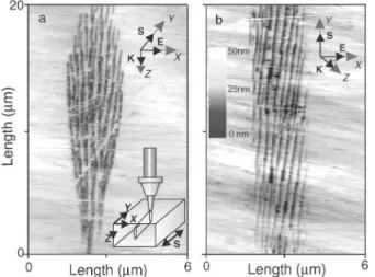
Optically produced arrays of planar nanostructures inside fused silica
Texte intégral
Figure

Documents relatifs
Abstract: We report on the formation of laser-induced periodic annular surface structures (LIPASS) on fused silica irradiated with multiple femtosecond laser
Time resolved side imaging of transient local changes in fused silica subsequent to ultrashort pulse irradiation is reported. A pump probe set-up enabled the monitoring
In conclusion, time-resolved transmission and XPM measure- ments have been performed on amorphous fused silica sam- ples excited by femtosecond SWIR laser pulses, and a
If it is as- sumed that there is a distribution of strain matrix elements and that they also determine the decay, then the electric echo involves the excitation of systems with
Nous proposons ici, de cumuler les avantages des deux schémas dans la même simulation numérique en couplant les deux approches : un code lagrangien calcule les parties présentant peu
In order to turn features (I-IV) into a model, we need three things: (i) an appropriate vocabulary of conversational moves for building sequences of message
At each water- Samples used for helium diffusion studies were solid ratio, nine sets of samples were prepared, also used for sulphur impregnation work.. Three
Réussir un test de problèmes impliquant les 4 opérations, un seul calcul (sans retenues) et des nombres < 100.. Réussir un test de problèmes impliquant les 4 opérations,
