Publisher’s version / Version de l'éditeur:
Journal of Applied Physics, 99, 12, p. 123502, 2006
READ THESE TERMS AND CONDITIONS CAREFULLY BEFORE USING THIS WEBSITE. https://nrc-publications.canada.ca/eng/copyright
Vous avez des questions? Nous pouvons vous aider. Pour communiquer directement avec un auteur, consultez la
première page de la revue dans laquelle son article a été publié afin de trouver ses coordonnées. Si vous n’arrivez pas à les repérer, communiquez avec nous à PublicationsArchive-ArchivesPublications@nrc-cnrc.gc.ca.
Questions? Contact the NRC Publications Archive team at
PublicationsArchive-ArchivesPublications@nrc-cnrc.gc.ca. If you wish to email the authors directly, please see the first page of the publication for their contact information.
NRC Publications Archive
Archives des publications du CNRC
This publication could be one of several versions: author’s original, accepted manuscript or the publisher’s version. / La version de cette publication peut être l’une des suivantes : la version prépublication de l’auteur, la version acceptée du manuscrit ou la version de l’éditeur.
For the publisher’s version, please access the DOI link below./ Pour consulter la version de l’éditeur, utilisez le lien DOI ci-dessous.
https://doi.org/10.1063/1.2201998
Access and use of this website and the material on it are subject to the Terms and Conditions set forth at
Physical properties of lanthanum monosulfide thin films grown on (100)
silicon substrates
Cahay, M.; Garre, K.; Wu, X.; Poitras, Daniel; Lockwood, David; Fairchild, S.
https://publications-cnrc.canada.ca/fra/droits
L’accès à ce site Web et l’utilisation de son contenu sont assujettis aux conditions présentées dans le site LISEZ CES CONDITIONS ATTENTIVEMENT AVANT D’UTILISER CE SITE WEB.
NRC Publications Record / Notice d'Archives des publications de CNRC:
https://nrc-publications.canada.ca/eng/view/object/?id=8273b776-a68c-48fc-876c-3d159a58c252 https://publications-cnrc.canada.ca/fra/voir/objet/?id=8273b776-a68c-48fc-876c-3d159a58c252共Received 24 October 2005; accepted 7 March 2006; published online 16 June 2006兲
Thin films of lanthanum monosulfide 共LaS兲 have been deposited on Si 共100兲 substrates by pulsed laser deposition. The films are golden yellow in appearance with a mirrorlike surface morphology and a sheet resistance around 0.1 ⍀ / 䊐, as measured using a four-probe measurement technique. The thin films are characterized by atomic force microscopy 共AFM兲, x-ray diffraction 共XRD兲 analysis, high resolution transmission electron microscopy 共HRTEM兲, ellipsometry, and Raman spectroscopy. The root-mean-square variation of 共1m thick兲 film surface roughness measured over a 1m2area by AFM was found to be 1.74 nm. XRD analysis of fairly thick films 共micrometer size兲 reveals the growth of the cubic rocksalt structure with a lattice constant of 5.863共7兲 Å, which is close to the bulk LaS value. HRTEM images reveal that the films are comprised of nanocrystals separated by regions of amorphous material. Two beam bright field TEM images show that there is a strain contrast in the Si substrate right under the interface with the LaS film and penetrating into the Si substrate. This suggests that there is an initial epitaxial-like growth of the LaS film on the Si substrate that introduces a strain as a result of the 8% lattice mismatch between the film and substrate. Ellipsometry measurements of the LaS films are well characterized by a Drude-Lorentz model from which an electron concentration of about 2.52⫻ 1022cm−3 and a mobility around 8.5 cm2/ V s are derived. Typical crystalline LaS features were evident in Raman spectra of the films, but the spectra also revealed their disordered 共polycrystalline兲 nature. © 2006 American Institute of Physics. 关DOI:10.1063/1.2201998兴
I. INTRODUCTION
Rare-earth monosulfides, in their rock salt structure, of-fer a more stable alternative to alkali metals in reaching low or negative electron affinity 共LEA/NEA兲 when deposited on, for example, various III-V semiconductor surfaces.1 Of par-ticular interest is the room temperature work function 共WF兲 of these chalcogenides. When extrapolated from high-temperature measurements,2these are found to be quite low 共around 1 eV兲. One therefore expects that these materials can be used to reach the NEA condition when deposited onto p-type semiconductors. One advantage of rare-earth sulfides is that many of them are closely lattice matched to most commonly studied III-V compounds. For instance, bulk lan-thanum monosulfide 共LaS兲 has a lattice constant 共5.857 Å兲 very close to the lattice constant of indium phosphide 共InP, 5.8688 Å兲. Neodymium sulfide 共NdS兲 has a lattice constant of 5.69 Å, very close to the lattice constant of gallium ars-enide 共GaAs, 5.6533 Å兲. Two other important features of the rocksalt form of these rare-earth monosulfides are their rela-tively high melting temperature 共⬎2000 ° C兲 and their fairly low electrical resistivity 共a few tens of⍀ cm兲.3
In 2001, Modukuru et al. reported the growth of bulk samples of LaS and NdS using the sesquisulfide route.4 A
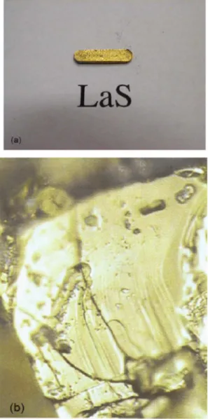
carbon reduction process during the high-temperature an-nealing portion of the growth process was shown to greatly reduce the presence of oxysulfide impurity phases 共La2O2S and Nd2O2S兲 in the samples.4A picture of a LaS pellet pre-pared in a high-temperature induction furnace from Thermal Technologies, Inc., is shown in Fig. 1. Several of these pel-lets were prepared using the carbon reduction technique until enough material was produced to form a 2 in. diameter 1 / 8 in. thick target which was then sintered in the high-temperature furnace. The resulting target was then used for pulsed laser deposition 共PLD兲 of LaS thin films. A prelimi-nary account of the growth of LaS films in their cubic rock-salt structure on 共100兲 Si substrates was reported recently.5In this paper, we give details of our investigation of the LaS thin films electrical and optical properties.
II. EXPERIMENT
In the PLD experimental set up,6the target to substrate distance was set equal to 5 cm and the high-vacuum chamber base pressure was about 8 ⫻ 10−8Torr. All the films were grown on polished 共100兲 silicon substrates, which were pre-pared using a standard cleaning procedure. A Lambda Physik LPX 305 excimer laser operating at a wavelength of 248 nm was used for the deposition. The beam spot size on the target was about 1 ⫻ 3 mm2, and the laser power was set to
a兲Electronic mail: marc.cahay@uc.edu
800 mJ/ pulse. Approximately 56% of the laser energy is at-tenuated by the time the pulse reached the target due to losses from beam steering optics and the chamber window. Thus the amount of energy per pulse reaching the target is approximately 355 mJ/ pulse. During deposition, the target was rotated on axis, while galvanometers were used to raster the laser beam in a uniformly random pattern over the sur-face of the target. This configuration produces a uniform la-ser plume by preventing uneven erosion of the target. A ho-mogeneous laser plume is critical for producing films with uniform thickness. Using a laser repetition rate of 40 Hz, with a substrate temperature of 100 ° C and no background gas pressure, the film growth was estimated to be about 20 nm/ min for the set of PLD parameters listed above. The thin films were characterized using x-ray diffraction 共XRD兲 at a grazing angle from 1° to 3° using a RIGAKU D-2000 model XRD machine. To investigate the texture of the films, cross-section transmission electron microscopy 共TEM兲 samples were prepared following standard procedures. Two bars were cut out of a wafer, and were glued together with
the LaS film sides face to face to make the central part of the 3 mm diameter cross-section sample disk. The disk was then mechanically thinned to ⬃100m thickness. The thinned disk was dimpled from both sides with 3m diamond paste until the center of the disk was ⬃20m thick, and then polished from both sides with 1m diamond paste to get a very smooth surface. The final thinning to produce sample perforation was conducted using Ar ion milling from both sides with an ion beam angle of 9° and a gun voltage of 6 kV. The TEM sample was examined in a Philips EM430T microscope operating at 250 kV. Variable-angle spectro-scopic ellipsometry 共VASE, J. A. Woollam Co., Lincoln NE兲 measurements were performed on the sample, from 275 to 1700 nm 共4.5– 0.73 eV兲, at six different angles of in-cidence ranging from 60° to 85°. The complex permittivity of the LaS film was extracted from the ellipsometric data, assuming that the film was homogeneous and no scattering. The Raman scattering experiments were carried out in an ambient atmosphere of helium gas at a temperature of 295 K in a quasibackscattering Brewster-angle geometry7 with the incident light at an angle of 77.7° from the normal to the LaS film surface. Spectra were excited with 150 mW of 457.9 nm argon laser light. The incident laser light formed a slit shaped spot of dimensions 1 ⫻ 0.1 mm2 on the sample, which to-gether with the use of the stream of He gas flowing over the sample in the laser spot area helped minimize the local laser heating. The light scattered at 90° 共external to the sample兲 was analyzed with a Spex 14018 double monochromator at a spectral resolution of 7.8 cm−1, and detected with a cooled RCA 31034A photomultiplier. The incident light was polar-ized in the scattering plane, while the scattered light was recorded without polarization analysis. Spectrometer calibra-tions were made immediately before and after each sample spectrum was recorded.
III. EXPERIMENTAL RESULTS
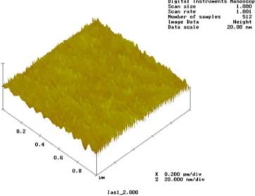
As shown in Fig. 2, the LaS films are golden yellow in appearance with a mirrorlike surface morphology. The sheet resistance of the thin films was measured to be about 0.1 ⍀ / 䊐 using a four-probe measurement result. As shown on a typical plot in Fig. 3, atomic force microscopy 共AFM兲 scans of the LaS film 共about 1m thick as determined by TEM analysis兲 over a 1m2area reveal a root-mean-square
FIG. 1. 共a兲 Picture of a LaS pellet about 1 in. long, 0.5 cm wide, and 5 mm thick formed prior to fabricating the LaS target for PLD deposition. 共b兲 Optical micrograph of one LaS pellet showing a microcrystal of LaS about 30m2in area.
FIG. 2. Picture of a LaS thin film grown by PLD on a 共100兲 Si substrate. The reflection of the finger clearly shows the metallic character of the thin film.
共rms兲 variation in the surface roughness of 1.743 nm. This high smoothness of the film was verified over the entire area of the sample shown in Fig. 2.
A. XRD results
Figure 4 shows a typical XRD scan of the golden-yellow LaS thin film. The XRD scan reveals principal Bragg reflec-tions of the cubic rocksalt phase. An analysis of the Bragg reflection peaks leads to a lattice parameter of a = 5.863共7兲 Å, which is very close 共0.1% larger兲 than the value we reported earlier for bulk samples, a = 5.857共2兲 Å.2–4 The observation of many Bragg reflection peaks suggests that the film is polycrystalline, which is to be expected be-cause of the large lattice mismatch 共about 8%兲 between the lattice constant of the LaS rocksalt phase and of the Si sub-strate 共a = 5.431 Å兲. Furthermore, the Bragg peaks are fairly broad suggesting the presence of polycrystalline grains of different sizes and potentially the presence of amorphous re-gions in the film. Using Scherrer’s equation,8,9the size of the
nanocrystalline grains in the film can be estimated from the full width at half maximum of the Bragg peaks while taking into account a linewidth correction for x-ray instrumentation broadening. Starting with the 共200兲 Bragg peak in Fig. 4 and using = 1.541 Å for the wavelength of the Cu K␣ line, the average size of the nanocrystalline grains in the LaS film is found to be about 12.7 nm. This estimate agrees well with cross-section TEM analysis of the LaS thin film, as described next.
B. TEM results
Figure 5 shows a 具011典 zone axis bright field cross-section TEM image 关Fig. 5共a兲兴 of the LaS films on the 共100兲 Si substrate, the corresponding electron diffraction pattern from both the LaS film and Si substrate 关Fig. 5共b兲兴, and the electron diffraction pattern from the LaS film only 关Fig. 5共c兲兴. The thickness of the film is measured from the image as 0.98m. In addition to the diffraction spots from the Si single crystal diffraction pattern of 具011典 zone axis, there are discontinuous rings as well in Fig. 5共b兲 that are from the LaS film, as shown in Fig. 5共c兲. The diffraction pattern of Fig. 5共c兲 means that the LaS film consists of nano/microcrystal and amorphous phases. This finding was confirmed by HR-TEM observations. Figures 6 and 7 are HRHR-TEM lattice
im-FIG. 3. AFM scan of a LaS thin film 共about one micron thick兲 grown on a 共100兲 Si substrate. The scan is over 1m2. The root mean square of the
surface roughness is 1.743 nm over that area.
FIG. 4. X-ray diffraction at three different grazing angles of incidence 共兲 from a LaS thin film deposited on a 共100兲 Si substrate. Miller indices 共hkl兲 of the reflections from the cubic rocksalt phase of LaS are identified. The peak located around 56° is due to the 共311兲 Bragg reflection observed for a bare Si substrate 共JCPSD Card No. 77-211兲.
FIG. 5. 共a兲 具011典 zone axis bright field cross-section TEM image of the LaS films on the 共100兲 Si substrate. 共b兲 Corresponding electron diffraction pat-tern from both the LaS film and Si substrate. 共c兲 Electron diffraction patpat-tern from the LaS film only.
FIG. 6. HRTEM image of the LaS / Si interface clearly showing the nano-crystalline and amorphous regions.
ages of the LaS film on the Si substrate. These images reveal the existence of randomly oriented nanocrystals and amor-phous regions in the proportion of approximately 60%–40%, respectively. A close inspection of the lattice image of the interface region in Fig. 7 shows an initial epitaxial growth of the LaS on the Si substrate. Figure 8 is a 具011典 bright field cross-section TEM image taken with g = 400. In this image, the band of dark contrast in the Si substrate is a measure of the residual strain evident in the LaS film. The strain in the LaS films could arise from the thermal mismatch during the cooling from the growth temperature to room temperature due to the different thermal expansion coefficients of the LaS film and Si substrate and/or from the initial epitaxial growth of the LaS film on Si substrate due to the different lattice parameters of LaS and Si. The lattice mismatch strain is 8% assuming that the lattice parameters are 5.863 and 5.431 Å for LaS and Si, respectively.
C. Ellipsometric characterization
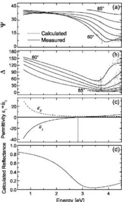
The measured ellipsometric dataand ⌬ of the LaS thin film are shown in Figs. 9共a兲 and 9共b兲, respectively. These spectra were modeled using Drude-Lorentz types of oscilla-tors: = ⬁− AD⌫D E2+ i⌫DE +
兺
n An⌫nEn En2− E2− i⌫nE = 1+ i2. 共1兲 The resulting permittivity dispersion curve fits very well the experimental data using two Lorentzians in the expansionabove with the values of the parameters listed in Table I, as shown in Fig. 9共c兲. The parameters ADand ⌫Din the Drude
term were used to extract the carrier concentration and the mobility of LaS, 2.52⫻ 1022cm−3 and 8.5 cm2/ V s, respec-tively, assuming an effective mass m*= 1.3m0.10 The carrier concentration is comparable with values given for bulk LaS.10In order to increase slightly the quality of the experi-mental fit, a 3.5 nm thick oxide layer was added to the model. From the permittivity values we deduced a minimum absorption coefficient ␣⬇ 138 cm−1 and a maximum pen-etration depth 1 /␣⬇ 70 nm, which was not large enough to probe information related to the LaS / Si interface. From the estimates of the electron concentration and mobility reported above and a measured film thickness of 0.98m, the sheet resistance of the thin film is calculated to be 0.29 ⍀ / 䊐, which is in good agreement with the four-probe measure-ment result.
For comparison with prior reports on LaS, a reflectance spectrum was calculated from the Drude-Lorentz model, as shown in Fig. 9共d兲. Its shape is typical of
monochalco-FIG. 7. Same as Fig. 6 at higher resolution.
FIG. 8. g = 400 bright field TEM image showing the strain contrast between the LaS and Si substrate interface.
FIG. 9. Ellipsometry parameters 共a兲共E兲 and 共b兲 ⌬共E兲 of a LaS thin film grown by PLD on a 共100兲 Si substrate. The continuous lines represent the fits to the experimental values 共dashed lines兲 using a Drude-Lorentz model. 共c兲 Extracted permittivity dispersion curves 1and 2of the LaS thin film.
共d兲 Expected reflectance spectrum of the LaS thin film calculated from the Drude-Lorentz model.
TABLE I. Parameters used in Eq. 共1兲 to fit the ellipsometric data 共with ⬁
= 2.5469兲.
Oscillator A 共eV兲 ⌫n共eV兲 En共eV兲
Drude 3.5514 7.5164 ¯
Lorentz 1 825.19 0.455 77 0.037 278
Lorentz 2 5.1043 0.287 54 5.1043
genides, and similar to published reflectance measure-ments,10,11with 共i兲 a metallic behavior below 2 eV due to the 5p quasi-free-electrons, 共ii兲 a drop of the reflectance around 3 eV due to a conduction-electron plasma oscillation inter-fering with interband excitations 共f → d , p → d兲, and 共iii兲 an increase of the reflectance at higher energies, mainly caused by 3p → 5d interband transitions.11An energy of 2.8 eV for the conduction-electron plasma resonance in the presence of interband transition is found, given by 1= 0.11This energy is slightly larger than the previously reported value of 2.6 eV for bulk LaS,10 may be due to the polycrystalline nature of the films.
D. Raman characterization
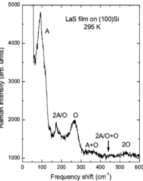
The Raman spectra of these Si:LaS films exhibit weak broad features extending out to 600 cm−1, as illustrated in Fig. 10. The results obtained are generally similar, but not in detail, to those found earlier from Raman measurements on bulk pure LaS samples,4,12confirming that the LaS films are pure and mostly crystalline. Strong peaks are observed at 91 and 264 cm−1, with weaker features at 120, 141, 174, 183, 365, 420, 455, and 532 cm−1.
One triply degenerate optical phonon mode, split into longitudinal 共LO兲 and transverse 共TO兲 components, is ex-pected for rare-earth monochalcogenides possessing the rocksalt crystal structure. First-order Raman scattering from phonons in such crystals is symmetry forbidden and usually a weak second-order Raman spectra is observed reflecting the two-phonon density of states 共DOS兲. However, previous Raman studies of other rare-earth chalcogenides13,14 have shown that disorder introduced by defects such as cation and/or anion vacancies14 can induce a first-order Raman spectrum reflecting the one-phonon DOS. The TEM analysis of our samples shows that structural disorder due to the for-mation of nanocrystals separated by amorphous material is also present. Thus the Raman spectrum of our LaS films can be expected to show both disorder-induced first-order as well
Xand K critical points in the Brillouin zone, while the shoul-der at 120 cm−1 comes mainly from L point TA and LA phonons. Unfortunately, the dispersion curves for LaS opti-cal phonons are not known, but by analogy with those found for yttrium monosulfide 共YS兲 共Ref. 16兲 only a small overall TO-LO splitting can be expected for LaS. Thus the main peak at 264 cm−1comprises contributions from both TO and LO phonons, with the highest frequency contributions from LO modes. The contributions from TO modes can extend to lower frequencies, and the broad feature near 183 cm−1 un-derlying the sharper feature at 174 cm−1could represent such contributions. A similar assignment has been made for other rare-earth chalcogenides from Raman spectroscopy12–14 and also from point contact spectroscopy,14but the assignment is not definite.12,13 This is because this so-called TO peak12 overlaps with second-order Raman scattering from acoustic modes. Such scattering is generally found to be quite strong in bulk rare-earth chalcogenides.4,12–14However, this is not the case in our thin films. From the neutron scattering results,15 the sharp peak at 174 cm−1can be associated with second-order Raman scattering from TA and LA phonons at the X point, where there is a sharp and strong peak in the one-phonon DOS. The underlying broad peak at 183 cm−1 referred to above could arise from second-order scattering from TA and LA phonons at the K point. The weak peak at 141 cm−1is of unknown origin.
The broad and very weak bands occurring at frequencies higher than the optic phonon peak are all second order in origin reflecting primarily combinations of the disorder-induced first-order DOS Raman peaks. For example, the peaks at 365, 455, and 532 cm−1 can be attributed to the combinations of the 91 and 120 共A兲 cm−1peaks with the 264 共O兲 cm−1 peak 共A + O兲, 2A / O + O 共see Fig. 10兲, and O + O, respectively.
IV. CONCLUSIONS
Thin films of lanthanum monosulfide 共LaS兲 have been deposited on Si 共100兲 substrates by pulsed laser deposition 共PLD兲. The films are golden yellow in appearance with a mirrorlike surface morphology and a sheet resistance below 1 ⍀ / 䊐. The root-mean-square variation of 共1m thick兲 film surface roughness measured over a 1m2area by AFM was found to be below 2 nm. XRD analysis reveals the success-ful growth of the cubic rocksalt structure with a lattice con-stant of 5.863共7兲 Å, which is close to the bulk LaS value. High resolution TEM 共HRTEM兲 images indicate that the films are comprised of nanocrystals separated by regions of amorphous material. Ellipsometry measurements of the LaS
FIG. 10. Room temperature Raman spectrum of a LaS film grown on 共100兲 Si. A and O refer to acoustic and optical phonons involved in first-order and second-order Raman scatterings.
films are well characterized by a Drude-Lorentz model from which an electron concentration of about 2.52⫻ 1022cm−3 and a mobility around 8.5 cm2/ V s are derived. Both crys-talline and disordered LaS features were evident in Raman spectra of the films.
These rare-earth sulfide thin films should have potential applications in vacuum microelectronics if they can be used to reach NEA/LEA at the surface of various III-V and II-VI compound semiconductors. Applications would include mi-crowave vacuum transistors and tubes, pressure sensors, thin panel displays, and high-temperature and radiation tolerant sensors.
1P. D. Mumford and M. Cahay, J. Appl. Phys. 79, 2176 共1996兲. 2The room temperature work function for LaS and NdS was calculated by
extrapolating measured work function values at high temperature 关S. Fo-menko, Handbook of Thermionic Properties 共Plenum, New York, 1966兲兴. Within the range of temperature investigated by Fomenko, the work func-tion increases with temperature at a rate of a few meV/K.
3G. V. Samsonov, High Temperature Compounds of Rare-Earth Metals
with Nonmetals 共Consultants Bureau Enterprises, Inc., New York, 1965兲.
4Y. Modukuru, J. Thachery, H. Tang, A. Malhotra, M. Cahay, and P.
Bool-chand, J. Vac. Sci. Technol. B 19, 1958 共2001兲.
5S. Fairchild, J. Jones, M. Cahay, K. Garre, P. Draviam, P. Boolchand, X.
Wu, and D. J. Lockwood, J. Vac. Sci. Technol. B 23, 318 共2005兲.
6D. B. Chrisley and G. K. Hubler, Pulsed Laser Deposition of Thin Films
共Wiley Interscience, New York, 1999兲.
7D. J. Lockwood, M. W. C. Dharma-Wardana, J.-M. Baribeau, and D. C.
Houghton, Phys. Rev. B 38, 2243 共1987兲.
8C. J. Doss and R. Zallen, Phys. Rev. B 48, 15626 共1993兲.
9R. Jenkins and R. L. Snyder, Introduction to X-ray Powder Diffractometry
共Wiley Interscience, New York, 1996兲, p. 90.
10W. Beckenbaugh, J. Evers, G. Büntherodt, E. Kaldis, and P. Wachter, J.
Phys. Chem. Solids 36, 239 共1975兲.
11V. N. Antonov, B. N. Harmon, and A. N. Yaresko, Phys. Rev. B 69,
094404 共2004兲.
12I. Frankowski and P. Watcher, Solid State Commun. 40, 885 共1981兲. 13G. Güntherodt, P. Grünberg, E. Anastassakis, M. Cardona, H. Hackfort,
and W. Zinn, Phys. Rev. B 16, 3504 共1977兲.
14A. Treindl and P. Wachter, Phys. Lett. 64A, 147 共1977兲.
15M. M. Steiner, H. Eschrig, and R. Monnier, Phys. Rev. B 45, 7183 共1992兲. 16P. Roedhammer, W. Reichardt, and F. Holtzberg, Phys. Rev. Lett. 40, 465
共1978兲.