Design Tool and Methodologies for Interconnect
Reliability Analysis in Integrated Circuits
by
Syed Mohiul Alam
S.M., Massachusetts Institute of Technology, 2001
B.S., The University of Texas at Austin, 1999
Submitted to the
Department of Electrical Engineering and Computer Science
in partial fulfillment of the requirements for the degree of
Doctor of Philosophy in Electrical Engineering and Computer Science
at the
MASSACHUSETTS INSTITUTE OF TECHNOLOGY
September 2004
c
° 2004 Massachusetts Institute of Technology
All Rights Reserved
Author . . . .
Department of Electrical Engineering and Computer Science
August 31, 2004
Certified by . . . .
Donald E. Troxel
Professor of Electrical Engineering and Computer Science
Thesis Supervisor
Certified by . . . .
Carl V. Thompson
Stavros Salapatas Professor of Materials Science and Engineering
Thesis Supervisor
Read by . . . .
Duane S. Boning
Associate Department Head and Professor of Electrical Engineering
and Computer Science
Thesis Reader
Accepted by . . . .
Arthur C. Smith
Chairman, Department Committee on Graduate Students
Design Tool and Methodologies for Interconnect Reliability
Analysis in Integrated Circuits
by
Syed Mohiul Alam
Submitted to the Department of Electrical Engineering and Computer Science on August 31, 2004, in partial fulfillment of the
requirements for the degree of
Doctor of Philosophy in Electrical Engineering and Computer Science
Abstract
Total on-chip interconnect length has been increasing exponentially with technology scaling. Consequently, interconnect-driven design is an emerging trend in state-of-the-art integrated circuits. Cu-based interconnect technology is expected to meet some of the challenges of technology scaling. However, Cu interconnects still pose a reliability concern due to electromigration-induced failure over time.
The major contribution of this thesis is a new reliability CAD tool, SysRel, for thermal-aware reliability analysis with either Al or Cu metallization technology in conventional and three-dimensional integrated circuits. An interconnect tree is the fundamental reliability unit for circuit-level reliability assessments for metallization schemes with fully-blocking boundaries at the vias. When vias do not block electro-migration as indicated in some Cu experimental studies, multiple trees linked by a non-blocking via are merged to create a single fundamental reliability unit. SysRel utilizes a tree-based hierarchical analysis that sufficiently captures the differences be-tween electromigration behavior in Al and Cu metallizations. The hierarchical flow first identifies electromigration-critical nets or “mortal” trees, applies a default model to estimate the lifetimes of individual trees, and then produces a set of full-chip reli-ability metrics based on stochastic analysis using the desired lifetime of the circuit.
We have exercised SysRel to compare layout-specific reliability with Cu and Al metallizations in various circuits and circuit elements. Significantly improved test-level reliability in Cu is required to achieve equivalent circuit-test-level reliability. The required improvement will increase as low-k dielectric materials are introduced and liner thicknesses are reduced in future.
Thesis Supervisor: Donald E. Troxel
Title: Professor of Electrical Engineering and Computer Science Thesis Supervisor: Carl V. Thompson
Dedication
To my mother Shahana Alam
Acknowledgments
I am grateful to my co-advisors Professors Donald E. Troxel and Carl V. Thompson for their guidance and support throughout the years at MIT. There were numerous discussions and meetings leading to the successful completion of this thesis. I would like to thank Professor Duane S. Boning for serving in my thesis committee. He provided valuable feedback during one-on-one and committee meetings.
This research was supported by Microelectronics Advanced Research Corporation (MARCO) Interconnect Focus Research Center Program. I got numerous opportuni-ties to actively participate in annual and quarterly reviews and to interact with other researchers and industry members in the program. I acknowledge the valuable inter-actions with Professor James Meindl, Professor Kenneth Goodson, Professor Anantha Chandrakasan, Professor Rafael Reif, Sungjun Im, Jae-Mo Koo, Eric Pop, and Tyrone Hill.
I would like to thank my colleagues at MIT, Frank Wei, Zung-Sun Choi, Ramku-mar Krishnan, Rajappa Tadepalli, and Andrew Takahashi, for their support through discussions and collaboration. This research is partially built upon prior work in our group. The Magic layout parsing and data storage in SysRel are based on Yonald Cherry’s earlier work with ERNI. Electromigration analysis in Cu metallization is based on experimental and modelling work by Gan Chee Lip, Frank Wei, and Zung-Sun Choi. Stefan Hau-Riege developed the concept of hierarchical reliability analysis with interconnect trees in Al metallization technology.
I was very fortunate for several summer internship opportunities during my gradu-ate studies. The thermal analysis work using ANSYS origingradu-ated during my internship at IBM T. J. Watson Research Center in Summer 2003. I am grateful to Kathryn W. Guarini and Meikei Ieong for giving me the opportunity to design the pilot testchip in 3D IC technology at IBM Watson Research.
My graduate school experience has been truly rewarding, both from academic and professional perspective. MIT fosters professional development and growth of its graduate student community through numerous programs and activities. I was the
Academics, Research, and Careers Committee Chair of the Graduate Student Council during the 2002-2003 academic year. I managed and led a group of graduate students in organizing major programs such as MIT Career Fair, Airport Shuttle Program, International Student Mentorship Program, Travel Grant Program, Academic Careers Series, and Professional Development Lecture Series. I would like to thank every one at the Graduate Student Council, and in particular, Emmi Snyder, for the wonderful experience.
Most importantly, I am indebted to the support and encouragement I have received over the years from my parents and family. I am grateful to my wife, Raiyan T. Zaman, for her love and dedication. I would like to thank my brother, Syed Masudul Alam, for his assistance in drawing many figures and for his support while writing this thesis.
Contents
1 Introduction 23
1.1 Interconnect Reliability . . . 24
1.1.1 Electromigration Phenomenon . . . 25
1.1.2 Electromigration Failure Modes . . . 27
1.1.3 Immortality Condition . . . 28
1.1.4 Electromigration Lifetime Model . . . 30
1.2 Interconnect Architecture Schemes . . . 31
1.2.1 Aluminum Metallization Technology . . . 31
1.2.2 Copper Metallization Technology . . . 31
1.3 Fundamental Reliability Unit . . . 32
1.4 Three-Dimensional (3D) Integrated Circuit Technology . . . 34
1.4.1 Technology Concept . . . 34
1.4.2 Layout Methodology for 3D Circuits . . . 35
1.4.3 3D IC Technology with Thermal Management . . . 36
1.4.4 Interconnect Reliability in 3D ICs . . . 38
1.5 Circuit-Level Reliability Analysis . . . 39
1.5.1 Electromigration Reliability in Networked Interconnects (ERNI and ERNI-3D) . . . 40
1.6 Thesis Statement . . . 41
1.7 Organization of Thesis . . . 42
2 Hierarchical Reliability Analysis Flow 45 2.1 Electromigration Experiments . . . 45
2.2 Via Asymmetric Failure Characteristics in Copper Technology . . . . 47
2.3 Steps in Hierarchical Reliability Analysis for Copper Metallization . . 49
2.4 Contrast with Hierarchical Reliability Analysis in Aluminum Metal-lization . . . 52
2.5 Electromigration Default Model . . . 53
2.6 Summary . . . 55
3 Electromigration Reliability Mathematics 57 3.1 Basic Definitions . . . 57
3.2 Lifetime Distribution Model . . . 61
3.2.1 Lognormal Distribution . . . 62
3.3 Reliability Mathematics in Series and Parallel Systems . . . 63
3.4 Reliability Metrics for Full-chip Analysis . . . 65
3.4.1 Probability of no failure . . . 66
3.4.2 Failure Rate along chip lifetime . . . 66
3.4.3 Time to cumulative % failure . . . 67
3.5 Reliability Metrics in Use . . . 67
3.6 Summary . . . 69
4 Electromigration Reliability Comparison of Aluminum and Copper Interconnects 71 4.1 Immortality Condition Filters . . . 72
4.2 Diffusivity Mechanisms and Models . . . 73
4.2.1 Diffusion in Aluminum Interconnects . . . 73
4.2.2 Diffusion in Copper Interconnects . . . 75
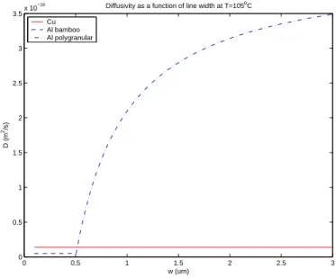
4.2.3 Diffusivity Comparison . . . 76
4.3 Lifetime Comparison of Straight Line Interconnects . . . 78
4.4 Reliability Prediction Using the ITRS . . . 81
5 SysRel: Circuit-Level Reliability CAD Tool 85
5.1 Software Architecture . . . 85
5.2 Graphical User Interface . . . 86
5.3 Circuit Layout Parsing . . . 88
5.4 Interconnect Tree Extraction . . . 90
5.5 Reliability Analysis Flow . . . 91
5.6 Simulation with 32-bit Comparator Layout . . . 93
5.6.1 Copper Metallization Technology . . . 95
5.6.2 Aluminum Metallization Technology . . . 96
5.7 Implications of SysRel . . . 96
5.8 Three-Dimensional IC Analysis in SysRel . . . 97
5.9 Summary . . . 100
6 Cell-Based Reliability Analysis in SysRel 101 6.1 Cell Characterization in SysRel . . . 102
6.2 Hierarchical Layout Support in SysRel . . . 103
6.3 Cell-based Reliability Simulation . . . 104
6.4 Computational Efficiency . . . 106
6.5 Summary . . . 107
7 Non-blocking Via Analysis in Copper Metallization Technology 109 7.1 Non-blocking Via Due to Liner Ruptures . . . 110
7.2 Non-blocking Via Assignment in Circuit Layout . . . 111
7.3 Steps for Non-blocking Via Analysis in SysRel . . . 112
7.4 Interconnect Tree Merging . . . 114
7.5 Line-length Effect on Reliability . . . 116
7.6 32-bit Comparator Layout Simulation . . . 118
7.7 Discussion of Results . . . 119
8 Thermal-Aware Reliability Analysis in SysRel 123
8.1 Fundamental Concepts for Thermal Analysis . . . 124
8.2 Thermal Simulation with ANSYS . . . 127
8.3 Transient Thermal Behavior in Integrated Circuits . . . 131
8.4 Cell-based Thermal Profiling Technique . . . 134
8.5 Interconnect Joule Heating . . . 138
8.6 Thermo-file Implementation in SysRel . . . 140
8.7 Thermal-Aware Reliability Simulation with 32-bit Comparator . . . . 141
8.8 Summary . . . 142
9 Reliability Analysis with Arithmetic and Logic Unit 145 9.1 Arithmetic and Logic Unit Design and Synthesis . . . 145
9.2 Reliability Simulation with Different Metallization Technologies . . . 148
9.3 Thermal-Aware Reliability Analysis with the 64-bit ALU . . . 152
9.4 Summary . . . 155
10 Conclusions and Future Work 157 10.1 Summary and Implications of Results . . . 160
10.1.1 SysRel: Interactive Reliability CAD Tool . . . 160
10.1.2 Thermal-Aware Reliability Analysis in SysRel . . . 163
10.1.3 Reliability Comparison of Copper and Aluminum Metallizations 164 10.1.4 Non-blocking Via Analysis with Copper Metallization . . . 165
10.2 Potential Applications of SysRel . . . 166
10.3 Future Directions . . . 167
10.3.1 Optimization of SysRel . . . 167
10.3.2 Enhanced Electromigration Lifetime Model . . . 168
10.3.3 Thermal Analysis and Management in 3D IC Technology . . . 169
10.3.4 Impact of Process Variations . . . 170
A SysRel Source Code Overview 171 A.1 Main Application Classes . . . 171
A.2 Graphical Interface Classes . . . 172
A.3 File Parser Classes . . . 173
A.4 Corner-stitched Data-structure Classes . . . 175
A.5 Layout and Tree Representation Classes . . . 175
A.6 Reliability Computation Class . . . 177
B Cadence to ANSYS Geometric Model Conversion: cds2inp 179 C Matlab Source Code for TProfile 189 D SysRel Release 193 D.1 SysRel v1.1 . . . 193
List of Figures
1-1 Cross-section of an Integrated Circuit showing multi-layer metal
inter-connects on top of a device layer. . . 24
1-2 Gate and interconnect delay, and interconnect reliability requirement in different technology generations . . . 25
1-3 Electromigration-induced failure modes . . . 27
1-4 Immortality Condition in a straight line interconnect . . . 28
1-5 Interconnect architecture schemes . . . 32
1-6 Example of an interconnect tree, the fundamental reliability unit for electromigration analysis . . . 33
1-7 Cross-section of a 3D IC with 3D trees and inter-wafer vias . . . 35
1-8 Different types of vias/contacts for 3D ICs . . . 36
1-9 Thermal management using optimal placement of microfluidic thermal connects in a face-to-face and back-to-back bonded 3D IC. . . 37
1-10 Flow diagram of the hierarchical circuit-level reliability analysis in ERNI 40 1-11 A screen-shot of MAJIC with a view of menu items for reliability anal-yses in ERNI . . . 41
2-1 Schematic diagrams of designed interconnect trees for electromigration testing . . . 46
2-2 Side-view schematic of void formation in via-above and via-below in-terconnects . . . 48
2-3 Calculating Lmax in an interconnect tree. . . 50
3-2 Schematic illustration of various system reliability models . . . 64
4-1 Cross-section of an Al interconnect with schematic illustration of dif-fusion pathways . . . 74
4-2 Cross-section of a Cu interconnect with schematic illustration of diffu-sion pathway . . . 75
4-3 A composite model of atomic diffusivity versus interconnect line width 77 4-4 Atomic diffusivity of Al and Cu metallization technologies at different temperatures . . . 78
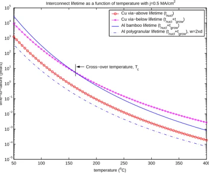
4-5 Interconnect lifetimes of various types of lines in Cu and Al metalliza-tion technologies . . . 80
4-6 Cross-over temperature versus current density plot . . . 80
4-7 Interconnect lifetimes of various types of lines in Cu and Al metalliza-tion technologies in typical operating condimetalliza-tion . . . 81
5-1 Screen shot of SysRel’s desktop pane . . . 87
5-2 Corner-stitched representation of a single plane with multiple tiles in a Magic layout . . . 89
5-3 Extraction of an interconnect tree from corner-stitched representation of tiles . . . 91
5-4 Reliability analysis flow diagram in SysRel . . . 92
5-5 The 32-bit comparator circuit layout analysis in SysRel . . . 94
5-6 Layout technique for Al polygranular to bamboo type conversion in an interconnect line . . . 97
5-7 The 3D 32-bit comparator circuit layout for SysRel reliability simulation 99 6-1 The largest cell, FAX1, characterization with SysRel . . . 103
6-2 Hierarchical layout view in SysRel . . . 104
6-3 Cell-based adder layout’s level 2 view in SysRel . . . 105
7-2 Straight line via-to-via Cu dual-damascene test structure for electro-migration experiments . . . 111 7-3 Menu options for reliability analysis in SysRel with non-blocking vias
in a circuit layout . . . 113 7-4 Schematic illustration of interconnect tree merging with a non-blocking
via . . . 114 7-5 Dynamic conversion of a non-blocking via into fully blocking in a
merged tree . . . 115 7-6 Illustration of interconnect tree merging in a 3-input nand gate layout 116 7-7 Time-to-failure dependence on interconnect length . . . 117 7-8 Mortal trees in the 32-bit comparator circuit layout when all vias are
assigned non-blocking . . . 120 7-9 Test structures to investigate the line length dependence of reliability
in Cu interconnects . . . 121 8-1 Z-axis dimensions with a substrate height of 10um in cds2inp . . . . 128 8-2 ANSYS thermal simulation with a bulk CMOS transistor . . . 130 8-3 Energy dissipation in the NMOS transistor of an inverter at different
output frequencies . . . 131 8-4 MOSFET transient temperature plot at 2.5M Hz square wave heat
generation frequency . . . 132 8-5 MOSFET transient temperature plot at 1GHz square wave heat
gen-eration frequency . . . 133 8-6 Package-level thermal modeling to compute uniform temperature at
the bottom surface of a substrate . . . 135 8-7 Thermal impulse response at the top surface of a substrate . . . 136 8-8 Power density profile of an inverter cell in a 30um × 30um substrate . 137 8-9 Temperature profile calculated using TProfile of an inverter cell in a
30um × 30um substrate . . . 137 8-10 Modeling the temperature profile in a straight line interconnect . . . 138
8-11 Modeling the temperature rise due to joule heating in multi-level
in-terconnects . . . 140
8-12 Thermo-file menu options in SysRel for thermal-aware reliability analysis141 8-13 Layout-level non-uniform temperature profile in the 32-bit comparator circuit layout . . . 142
9-1 The 64-bit Arithmetic and Logic Unit layout in Magic . . . 147
9-2 Immortality in interconnect trees in the 64-bit ALU circuit with Cu metallization . . . 148
9-3 Nonuniform temperature profile of the 64-bit ALU circuit in bulk CMOS technology at V dd = 5V and operating frequency= 250M Hz . 153 10-1 Straight line interconnect and interconnect tree structures in circuit layout . . . 158
10-2 Screen shot of SysRel desktop pane . . . 161
10-3 Multiple vias at a junction in wide metal interconnects . . . 169
List of Tables
3.1 Tree types with lognormal lifetime distribution . . . 68 3.2 Improved tree types with lognormal lifetime distribution . . . 68 3.3 Full-chip reliability metrics of circuit layout with various types of
mor-tal trees . . . 68 4.1 Reported (jL) product thresholds for immortality conditions in Al and
Cu technologies . . . 72 4.2 Immortality length in various technology generations with Al and Cu
metallizations . . . 73 4.3 Material parameters used for calculating diffusivity of Al polygranular
type lines . . . 74 4.4 Material parameters used for calculating diffusivity of Al bamboo type
lines . . . 75 4.5 Material parameters used for calculating diffusivity in Cu metallization
technology . . . 76 4.6 Technology-specific parameter description and values for lifetime
cal-culation . . . 79 4.7 Worst case interconnect lifetimes of various types of Cu and Al lines . 82 5.1 Menu bars and corresponding operations in SysRel . . . 88 5.2 A sample .mag layout file . . . 89 5.3 SysRel simulation results of hierarchical reliability analysis with Cu
5.4 SysRel simulation results of hierarchical reliability analysis with Al metallization in the 32-bit comparator circuit layout . . . 96 5.5 SysRel simulation results of hierarchical reliability analysis with Cu
metallization in the 3D 32-bit comparator circuit layout . . . 98 6.1 Cell reliability characterization data format in sysrelcell.char file . . . 102 6.2 Statistics of Fundamental Reliability Units in the 4-bit adder layout . 105 6.3 Statistics of Fundamental Reliability Units in the 32-bit comparator
circuit layout . . . 106 6.4 Time required for layout drawing in SysRel . . . 107 6.5 Time required for extracting interconnect trees in SysRel . . . 107 6.6 Computational efficiency with cell-based reliability analysis in SysRel 107 7.1 Input parameters for non-blocking via analysis defined in sysrel.emparam
file . . . 112 7.2 Reliability simulation with various degrees of non-blocking vias in the
32-bit comparator circuit layout . . . 119 8.1 Electrical and thermal analogy for modeling steady-state heat flow . . 125 8.2 Material parameters for thermal simulation in ANSYS . . . 129 8.3 Maximum temperature increase due to interconnect joule heating in
different technology generations . . . 140 8.4 Thermal-aware reliability simulation results with Cu metallization in
the 32-bit comparator circuit layout . . . 143 9.1 Operations in the 64-bit Arithmetic and Logic Unit . . . 146 9.2 The number of cells of various types in the 64-bit ALU circuit . . . . 147 9.3 Full-chip reliability analysis with the 64-bit ALU in different
metalliza-tion technologies . . . 149 9.4 Times to void nucleation and void growth in various interconnect
9.5 Cu atomic diffusivity requirements for equivalent circuit-level reliabil-ity in the 64-bit ALU with Al and Cu metallizations . . . 151 9.6 Thermal-aware full-chip reliability report for the 64-bit ALU with Cu/SiO2
metallization in bulk CMOS technology . . . 154 9.7 Thermal-aware full-chip reliability report for the 64-bit ALU with Cu/SiO2
Chapter 1
Introduction
In the pursuit of higher performance and integration, Integrated Circuit (IC) technol-ogy is heading towards the nanotechnoltechnol-ogy era. The gate length of a state-of-the-art active device, such as a metal oxide silicon field-effect transistor (MOSFET), is in the range of 45 to 50 nm allowing millions of such devices to be fabricated in a single chip [1]. In addition to achieving higher density, smaller devices increase speed due to higher drive current during the “on” state. While more and more devices are desirable for integrating more functionality in a single chip, interconnecting the devices using metal wires takes up an even greater percentage of space. The on-chip metal lines referred to as interconnects are fabricated by deposition of metal and dielectric mate-rials, lithography of patterned features, and selective etching. ICs can have up to 14 layers of metal interconnects as predicted by the International Technology Roadmap for Semiconductors (ITRS) 2003 edition (figure 1-1) [2]. The dielectric material, re-ferred to as inter-layer dielectric (ILD), provides insulation between interconnects and mechanical stability for the multi-level interconnect structure.
Concurrent to device dimension scaling, interconnect width is shrinking while total interconnect length is increasing exponentially. According to the International Tech-nology Roadmap for Semiconductors, 688 meters of active metal wiring per centimeter square area are required to construct a high-performance chip in 2004. Interconnect delay related to its resistance (R), capacitance (C), and in some cases inductance (L) has become dominant over gate delay as shown in figure 1-2(a). Moreover, the
Figure 1-1: Cross-section of an Integrated Circuit showing multi-layer metal intercon-nects on top of a device layer. Source: the ITRS [2].
increased capacitance in interconnects leads to an increase in net switching power. Since the invention of ICs, Aluminum (Al) and its alloys have been used in the met-allization layers. Silicon Dioxide (SiO2) is used as the ILD material. Copper (Cu)
has been replacing Al as the material of choice for interconnects due to its lower sheet resistance while new ILDs with lower dielectric constant (low-k dielectrics) are under active study. However, as seen in figure 1-2(a), interconnect delay is still dom-inant with the introduction of Cu and low-k dielectrics beyond 180nm technology generations. Therefore, interconnect design and analysis have become as important as device design [3].
1.1
Interconnect Reliability
From the interconnect design perspective, reliability is the extent to which the inter-connects maintain signal integrity and produce desired functionality over the lifetime
600 500 400 300 200 100 Generation (nm) (a) 40 30 20 10 0 De lay (ps )
gates and Al/SiO2
Al/SiO2
gates and Cu/low-k Cu/low-k
total gate delay
4000 6000 8000 10000 12000 Total Interconnect Length (m/cm )2 Year 2001 2002 2003 2004 2005 2006 2007 1.2 1.0 0.8 0.6 0.4 (FIT s/m length/ cm )x 10 2 -2 (b)
Figure 1-2: (a) Gate and interconnect delay in different technology generations [4]. (b) Interconnect reliability requirement versus total interconnect length in different years. Here F IT refers to Failure Unit. Source: the ITRS 2001 edition [2].
of a chip. Stress conditions, such as current density and temperature, during cir-cuit operation affect the interconnect reliability. As the performance of present day ICs increases, a more stringent operating condition in the metal interconnects is ex-pected with a service temperature of 105oC and maximum current density of 0.5
M A/cm2
[2]. In addition, the interconnect reliability requirement has become more stringent as shown in figure 1-2(b). Electromigration is the primary interconnect reliability concern.
1.1.1
Electromigration Phenomenon
Electromigration is the transport of atoms in a conducting material due to momentum transfer from flowing electrons. When a difference in electrical potential is applied to an interconnect, electrons flow from low potential (cathode) to high potential (anode) terminal. The metal atoms start to diffuse along the electron flow direction due to scattering. Assuming that the electron flow direction has a positive sign, the “electron wind” force on atoms can be expressed as
Felec = −q ∗
E = −Z∗
where q∗
= Z∗
e is the effective atomic charge, Z∗
is the effective atomic charge number, e is the fundamental electron charge, E = ρj is the electric field, ρ is the electrical resistivity of the metal, and j is the current density. As current density opposes the electron flow direction, a negative sign for j attributes to a positive sign in Felec.
In an interconnect terminating at diffusion barriers such as Tungsten (W ) filled vias or Tantalum (T a) liners, the “electron wind” force creates tensile stress near the cathode where the atoms deplete and compressive stress near the anode where the atoms accumulate [5]. The resulting stress gradient leads to a mechanical driving force, referred to as the back-stress force, which opposes the electromigration wind force. The back-stress force is expressed as
Fmech= Ω
dσ
dx (1.2)
where Ω is the atomic volume, σ is the stress, and x is the distance measured along the length of the line. Due to a negative value of dσ
dx, Fmech has a negative value which
is consistent with our sign convention here.
According to the 1-D Korhonen model [6], the atomic flux, Ja, can be expressed
as a function of Felec and Fmech using
Ja = DCa kT (Felec+ Fmech) = DCa kT (−Z ∗ eρj + Ωdσ dx) = −DCkTa(Z∗ eρj − Ωdσdx) (1.3) where Cais the atomic concentration, D is the atomic diffusivity, k is the Boltzmann’s
constant, and T is the temperature. Equation 1.3 suggests that |Felec| > |Fmech| is
1.1.2
Electromigration Failure Modes
A void nucleates at the cathode end of an interconnect line when the tensile stress ex-ceeds the critical stress necessary for void nucleation, σcrit nuc. Once a void nucleates,
it can grow to larger volume even spanning the whole interconnect width as shown in figure 1-3(a). In both Al and Cu metallization schemes, void nucleation and growth would result in a resistance increase of the line. In the event of a fully spanning void, conductive refractory metal under layers or over layers in Al technology will shunt the current to prevent an open-circuit failure. An open-circuit failure is more common in Cu technology due to the absence of conductive refractory layers. While an open-circuit due to voiding would cause functional failure, the resistance increase would add extra delay in signal propagation resulting in timing violations in timing critical circuits.
Figure 1-3: Electromigration-induced failure modes; (a) Tensile stress at the cathode-end of an interconnect can cause voiding [7]; (b) Compressive stress at the anode-cathode-end can cause extrusion [8].
Compressive stress at the anode end of both Cu and Al interconnect lines can cause metal extrusion where the atoms accumulate (figure 1-3(b)). However, extru-sions are not observed in service operating condition for either Al or Cu as metal interconnects are surrounded by rigid ILD material that suppresses the formation of hillocks. Current densities greater than 5 M A/cm2
are required to observe extrusion during electromigration testing condition [9]. Therefore, voiding is the primary mode
of electromigration failure in ICs.
1.1.3
Immortality Condition
In steady state, the “electron-wind” force balances the back-stress force resulting in zero atomic flux and a linear time-invariant stress along the interconnect line as illustrated in figure 1-4 [10]. Equation 1.3 in steady state becomes
Z∗ eρj = Ωdσ dx (1.4) tensile compressive Side view Top view cathode anode
Stress evolution with time (c) (b) (a) σcrit_nuc σcrit
x
F
mech∂
∂
Ω
=
σj
e
-Z
F
elec=
* ρ σo σextFigure 1-4: Immortality Condition in a straight line interconnect. (a) Side view (b) Top view (c) Stress as a function of location along the interconnect at different times. Rewriting equation 1.4 for a straight line interconnect with length, L, we can get
an expression for current density and line length product (jL) jL = Ω∆σmax
ρeZ∗ (1.5)
where ∆σmax is the maximum stress difference between the cathode and anode ends.
If the stress at the cathode end is σcrit, ∆σcrit can be written as
∆σcrit= 2(σcrit− σo) (1.6)
Assuming the initial stress, σo, is zero,
∆σcrit= 2σcrit (1.7)
If the critical tensile stress for void nucleation, σcrit nuc, is greater than the maximum
steady state tensile stress, σcrit, developed at the cathode end, no void will form and
the line will not fail. Using equation 1.5, we can derive a critical current density line length product (jL) that defines the immortality condition as
jL < (jL)crit nuc =
Ω∆σcrit nuc
ρeZ∗ (1.8)
which means short lines or lines stressed at low current densities that satisfy (jL) < (jL)crit nuc are immune from void nucleation, and thus “immortal” from void
nucle-ation limited failure.
On the other hand, if (jL) exceeds (jL)crit nuc, a void will nucleate in the metal
line. However, if the void does not completely block the current flow, the void nucle-ation will not be fatal. In the presence of conducting over layers and under layers, the void can continue to grow as the current is shunted around it through the refractory metal layers until the electron wind force and back-stress balance again. Under such circumstances, the line is immortal if the resistance increase associated with the void volume is lower than the maximum acceptable resistance increase, ∆Rmax
crit, and the
sur-rounding dielectric material. The immortality condition due to resistance saturation is given by [11] (jL)crit sat= ρ A ρl Al ∆Rmax crit R 2ΩB Z∗ eρ (1.9)
where ρ and A are the resistivity and cross sectional area of the high-conductivity metal, respectively, ρl and Al are the resistivity and cross sectional area of the shunt
layer, respectively, and R is the initial resistance of the line. It is apparent that (jL)crit sat > (jL)crit nuc as resistance saturation will occur after void nucleation.
1.1.4
Electromigration Lifetime Model
Electromigration testing is conducted at accelerated conditions with temperatures as high as 300oC and current densities greater than 2.0 M A/cm2
. To estimate the lifetime of a population of interconnects at service conditions, the well known Black’s equation is used to extrapolate the median-time-to-failure (MTTF) to service condi-tions [12]. Black’s equation is expressed as
t50 = Aj −n
eEakT (1.10)
where A is a constant independent of temperature and current density, j is the current density, n is the current density exponent, Ea is the activation energy for the
rate-limiting diffusion path, k is the Boltzmann’s constant, and T is the temperature. A current density exponent n = 1 is consistent with void growth limited failure since the rate of unconstrained void growth is proportional to the current density [13]. An exponent n = 2 indicates void nucleation limited failure in the model based on the Korhonen analysis [6]. Although variations of the original Black’s model have been proposed in [14, 15], Black’s equation is still generally used to estimate the lifetime of an interconnect due to electromigration.
1.2
Interconnect Architecture Schemes
Al and Cu are the primary choices of metal for interconnects in modern day ICs. IBM introduced Cu technology in commercial ICs in 1998. Since then, Cu has been replacing Al as the material of choice for interconnects due to its lower sheet resis-tance. While the electromigration behavior of Al interconnects is quite well under-stood [16, 17], the reliability of Cu is still under active study. Due to the differences in chemical properties between Cu and Al, the fabrication process for Cu interconnects is drastically different from that for Al interconnects. The differences in processing and architecture schemes lead to the differences in electromigration reliability.
1.2.1
Aluminum Metallization Technology
As illustrated in figure 1-1, metal interconnects are surrounded by ILD materials most commonly SiO2. Al chemically reacts with SiO2 to form alumina, which eliminates
atomic diffusion of Al into the surrounding ILD and along the interface between Al and SiO2. As a result, Al metallization is processed by a subtractive etching
method in which the patterned lines are formed by etching the deposited blanket Al film. Architecturally, Al interconnects have thick, highly electromigration-resistant refractory metal layers, which are usually made of Titanium Nitride (T iN ), serving as anti-reflection coatings at the top of the lines (see figure 1-5(a)). Similar under layers have also been included, which serve as seed layers for the via-fill process. Tungsten (W ) filled vias are used to connect layers of Al metallization. Metal under and over layers serve as shunt for electron flow and W -filled vias serve as fully blocking boundaries for electromigration.
1.2.2
Copper Metallization Technology
Cu does not chemically reduce SiO2 like Al does. Furthermore, a suitable etchant for
Cu thin films is unavailable for commercial use. Consequently, Cu interconnects are fabricated by the damascene method, in which a trench is first etched into a blanket layer of ILD before filling it with Cu by electroplating. Since Cu undergoes field
Figure 1-5: Interconnect architecture schemes; (a) Al interconnect, with W -filled vias and conducting shunt layers at the top and bottom of the interconnect line. (b) Dual-damascene Cu interconnect, with Cu-filled vias, thin refractory liners at the sides and bottom of the line, and a dielectric capping layer at the top of the line.
enhanced diffusion in most dielectric materials (including SiO2), in order to prevent
Cu atoms diffusing into the device layer, thin refractory metal layers consisting of Tantalum (T a) or Tantalum Nitride (T aN ) are placed at the sides and bottom of the Cu interconnect lines (See figure 1-5(b)). The Cu lines are capped with a dielectric diffusion barrier, which is usually made of Silicon Nitride (Si3N4). Cu-filled vias are
used to connect multiple layers of metallization.
1.3
Fundamental Reliability Unit
An important concept in hierarchical reliability analysis is the classification of Funda-mental Reliability Units (FRU). By definition, an FRU is a component in reliability analysis, contributing to the underlying failure mechanism, which can be treated in-dependently from other such components. During a hierarchical reliability analysis, FRUs are first identified and extracted from a circuit layout. FRU based reliability analysis reduces the complexity of the problem and provides the flexibility of adding new failure units for different reliability phenomena.
work. However, in real circuits, multiple straight line segments are connected at junc-tions and many such juncjunc-tions are connected within the same layer of metallization. An “interconnect tree” is a unit of continuously connected high-conductivity metal ly-ing within one layer of metallization terminatly-ing at the vias or diffusion barriers [18]. An example of an interconnect tree is shown in figure 1-6.
Figure 1-6: Example of an interconnect tree, the fundamental reliability unit for elec-tromigration analysis.
It has been established that an interconnect tree is the appropriate fundamen-tal reliability unit for the circuit-level reliability assessment of Al-based mefundamen-talliza- metalliza-tion [18]. The fully blocking boundaries formed at the W -filled vias confine atomic diffusion within an interconnect. Materials within an interconnect tree can diffuse freely between the segments and the stress evolutions in different segments of a tree are coupled.
On the other hand, Cu-filled vias with thin liner material at the bottom in Cu metallization technology may or may not act as fully blocking boundary for atomic diffusion [10]. Liner ruptures have been observed in some experimental work which allow materials to freely diffuse between different layers of metallization. In such cases an interconnect tree cannot be treated as the fundamental reliability unit for Cu-based technology.
1.4
Three-Dimensional (3D) Integrated Circuit
Tech-nology
Technology scaling has posed limitations on overall system performance by degrading the interconnect delay, increasing the power consumption due to interconnect capac-itance, and increasing the number of longer global and semi-global lines in a chip. The need for a long-term solution to enhance performance in successive technology generations is apparent. One such long-term solution is the three-dimensional (3D) Integrated Circuit technology.
1.4.1
Technology Concept
The main idea behind 3D integration is to form multiple device layers along the third axis (z axis) and lower the interconnect lengths by connecting the devices in these layers vertically. This has been accomplished by bonding multiple wafers fabricated with different or similar technologies [19, 20] as well as by fabricating multiple device layers on the same wafer [21, 22] using the epitaxial growth of Si. In a wafer bonding technology, each device-interconnect layer is fabricated separately on different wafers with the same or different technologies, and then the wafers are bonded with each other using a bonding layer of Cu, polymeric adhesives, or plain oxide-to-oxide (ILD material) bond.
The wafers in a 3D stack are electrically connected using high aspect ratio vias or contacts. When bonding is complete, 3D ICs have vertical interconnects of sig-nificantly longer length than vias or contacts in conventional or 2D ICs. Moreover, the 3D circuits fabricated with a wafer bonding technology have two different types of vertical interconnects as shown in figure 1-7. The Cu-filled inter-wafer vias con-nect multiple interconcon-nect trees from different wafers. At the bonding surface, the adjacent metallization layers from two wafers can also be connected with vertical Cu lines. The vertical Cu lines create a new type of trees, referred to as a “3D tree”, which expands between two different wafers.
Figure 1-7: Cross-section of a 3D IC with 3D trees and inter-wafer vias. Here DL and MLs correspond to device and metal layers, respectively.
Although the concept of 3D integration emerged as early as 1979 [23], significant research work was done only after the early 90’s as the limitations of technology scaling became apparent. 3D integration is an attractive solution as it can signifi-cantly reduce the number of long wires by mapping a 2D circuit into different lay-ers [24]. Moreover, the total number of repeatlay-ers for long and intermediate wires will also decrease, resulting in a higher density and lower interconnect-limited chip area. Consequently, high-performance microprocessors and programmable logic devices are attractive applications for 3D integration.
Another promising advantage of 3D integration is its ability to integrate heteroge-neous technologies into a single 3D chip. Future system-on-chip (SOC) applications will consist of digital, analog, RF, and optical components on the same die [25]. Using 3D integration, each unit can be fabricated on separate wafers with its own optimized process technology, and then integrated vertically to form a 3D SOC [19, 20].
1.4.2
Layout Methodology for 3D Circuits
We developed a comprehensive layout methodology for 3D ICs and implemented it in 3D-Magic [26, 27]. In order to facilitate the layout of 3D ICs, all inter-wafer vias or contacts are generalized into three major categories. The three categories of vias are sufficient for defining almost all types of interconnection between wafers in a 3D IC. Figure 1-8 shows the three categories of vias; top, connected-to-bottom, and through-wafer vias. Categorizing vias in such a way allows the layout methodology to be flexible enough to support different types of bonding schemes,
such as face-to-face, face-to-back, or back-to-back1 . A 3D contact point Connected-to-top Via Through-Wafer Via Connected-to-bottom Via Top Bottom
Figure 1-8: Different types of vias/contacts for 3D ICs.
The availability of 3D-Magic has led to interesting research with a wide range of layout-specific circuit analyses, from performance comparison of 2D and 3D circuits to layout-specific reliability analyses in 3D circuits. Using 3D-Magic, researchers have designed and simulated an 8-bit encryption processor mapped into 2D and 3D FPGA layouts [28]. The layout methodology has been adopted for 3D CAD tool research at MIT [29] . It has built the bridge between synthesis and layout tools for 3D circuits and allowed the demonstration of physical layouts of circuits produced by the 3D place and route tool. Moreover, it is an essential element of a novel Reliability Computer Aided Design (RCAD) tool, ERNI-3D [26].
1.4.3
3D IC Technology with Thermal Management
While 3D IC technology has its advantages, extracting heat generated by power dissi-pation in inner wafers is quite a challenge. Conventional packaging technology allows heat extraction from one side, typically the Si-substrate side, by attaching a Cu heat spreader and fin heatsink. When using such a method for heat extraction, heat flux from wafers further away from the heatsink would flow through the 3D stack leading
1
Face-to-face bonding refers to bonding metal interconnect side of a wafer to the metal intercon-nect side of another wafer while forming the 3D IC stack. Back-to-back bonding refers to bonding Si-substrate side of a wafer to the Si-substrate side of another wafer in forming the 3D IC stack.
to an increased power density on a smaller footprint. Therefore, temperature rise in 3D circuits can be significantly higher than that in conventional ICs [30].
Flexibility in bonding schemes, such as back-to-back and face-to-face, can be ex-ploited to address thermal management in 3D ICs. We proposed a vision for 3D IC technology that efficiently incorporates thermal management [31]. Figure 1-9 presents the main idea in such a 3D IC technology.
to External Pins Through-wafer via Heat Sink Device Layer 4 Device Layer 3 Device Layer 2 Metal Layer 1 & 2 Device Layer 1
Top view of thermal connect and through-wafer interconnect
Back-to-Back bond -through-wafer electrical connections and -Thermal connects for micro-channel fluid flow Face-to-Face bond with high density of bonded interconnect
Figure 1-9: Thermal management using optimal placement of microfluidic thermal connects in a face-to-face and back-to-back bonded 3D IC.
Starting at the bottom of the stack, there is a face-to-face bond between the first two wafers. This face-to-face bond allows high-density inter-wafer connection and eliminates area trade-off between through-wafer via and active devices that is present in back-to-back (substrate-to-substrate) or face-to-back bonding. In the figure, there are through-wafer vias through the substrate of the first wafer to get signals out for the connections to external pins. The number of such through-wafer vias is comparable to the number of pins and significantly lower than that of inter-wafer vias at a
high-density face-to-face bond.
Next, wafer no. 2 is bonded with wafer no. 3 using a to-back bond. This back-to-back or substrate-to-substrate bond results in a bonded silicon interface which can be used to contain micro-channels, termed thermal connects, for heat removal with fluid flow. The thermal connects or micro-channels are wet-etched in the back of the individual substrates before bonding. The thermal connects can be criss-crossed among through-wafer vias, as shown in figure 1-9, as well as laid out manually with a higher density at the chip hotspots.
The 3D stack can grow further upward using a face-to-face bond with wafer no. 3. In figure 1-9, the topmost wafer is wafer no. 4 and its substrate is connected to a heat sink/heat removal device. As it is apparent from the structure, every wafer in the 3D stack except wafer no. 1, has a heat removal device connected to its substrate. Therefore, thermal connects can also be placed in the substrate of wafer no. 1 while bonding to the package. Thus, every wafer in a 3D stack has heat removed through its substrate and the heat removal problem can be reduced to that of a conventional 2D IC.
1.4.4
Interconnect Reliability in 3D ICs
Electromigration phenomenon and reliability concerns described in section 1.1 are equally applicable to 3D circuits. In addition to treating interconnect trees as the fundamental reliability unit, special attention is required for the through-wafer and inter-wafer vias in 3D circuits. Through-wafer vias can be significantly longer in height than conventional vias as illustrated in figure 1-9. The reliability impact due to increased height as well as the presence of a bonded interface is under active investigation [32]. Depending on the failure characteristics observed in through-wafer and inter-wafer vias, it may be necessary to treat them as additional fundamental reliability units in 3D ICs.
As discussed earlier, the stack effect in 3D circuits can potentially increase the service temperature of the interconnects. According to equation 1.10, MTTF of an interconnect tree is exponentially dependent on its temperature. Due to high
power dissipation, high temperature rise is already of great concern in modern day conventional ICs. Consequently, the 3D counterparts of such chips are expected to pose a greater reliability challenge due to higher temperature.
1.5
Circuit-Level Reliability Analysis
The conventional approach to meet reliability goals in an integrated circuit has been to use simple and conservative design rules based on current density in a wire segment. However, this simplicity and conservatism lead to limited performance in newer tech-nology generations [18]. Models and techniques have been developed to make realistic reliability assessments of interconnects during the design and layout process (Relia-bility Computer Aided Design, RCAD), so that the relia(Relia-bility data can be fed back, and changes can be made promptly before the fabrication process to achieve optimum reliability and performance. BERT (BErkeley Reliability Tool) [33], iTEM [34], ERNI (Electromigration Reliability in Networked Interconnects) [35], and ERNI-3D [27] are examples of reliability analysis tools for Al-based interconnect technology that have been previously developed.
BERT and iTEM calculate the overall reliability of a given layout based on the reliability estimations from individual straight line segments. However, the reliabil-ity of a segment depends strongly on the activities in the linked segments. In other words, segments can not be treated as independent reliability units. Interconnect trees need to be considered as the fundamental reliability units as discussed in sec-tion 1.3. Another limitasec-tion in BERT and iTEM is the lack of immortality checking in interconnect segments. As illustrated in section 1.1.3, not all interconnect trees are prone to electromigration failure. Neglecting immortality condition in intercon-nect trees leads to redundant computation in analysis, and more importantly, leads to overly conservation and incorrect reliability estimates. ERNI and ERNI-3D addresses the limitations of earlier tools.
1.5.1
Electromigration Reliability in Networked Interconnects
(ERNI and ERNI-3D)
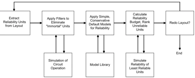
The RCAD tool ERNI (Electromigration Reliability in Networked Interconnects), developed at MIT [35], allows process-sensitive and layout-specific reliability assess-ments of a fully or partially laid-out integrated circuit. Figure 1-10 shows the flow diagram of ERNI’s operations. First, the interconnect trees are extracted from a
Extract Reliability Units from Layout Apply Filters to Eliminate "Immortal" Units Apply Simple, Conservative Default Models for Reliability Calculate Reliability Budget, Rank Unreliable Units Redo Layout? Simulation of Circuit Operation Model Library Simulate Reliability of Least Reliable Units End
Figure 1-10: Flow diagram of the hierarchical circuit-level reliability analysis in ERNI.
circuit layout and categorized into mortal and immortal trees based on the current density and line length product (jL). Further computation goes on with only the mortal trees, and a reliability figure for each tree, in terms of MTTF, is obtained after applying the default electromigration model [18].
The code for ERNI is written in Java 2 (JDK 1.2). It is a client extension to MAJIC, a layout parser and viewer also written entirely in Java [36]. Lots of data-structures and algorithms in MAJIC are based on MAGIC, an IC layout editor de-veloped at UC Berkeley and widely used in academia [37]. Using MAJIC, users can view a circuit layout, and apply reliability analysis by choosing different filtering algo-rithms from the “ERNI” menu. Figure 1-11 shows a screen-shot of MAJIC with the display of available options in the “ERNI” menu. ERNI operates on 2D IC layouts with multiple metallization layers created using MAGIC.
Figure 1-11: A screen-shot of MAJIC with a view of menu items for reliability analyses in ERNI.
RCAD tool, 3D, for the reliability analysis of 3D circuits [27]. Using ERNI-3D, circuit designers can get interactive feedback on the reliability of their circuits associated with electromigration, 3D bonding, and joule heating. ERNI-3D parses 3D circuit layouts from 3D-Magic and extracts both conventional and 3D interconnect trees from the layouts. It employs the hierarchical reliability analysis approach used in ERNI and applies a simplistic joint probability distribution method to report a single reliability figure for the whole chip. The initial version of ERNI-3D treats 3D circuits with two wafers or device-interconnect layers in the stack. Both ERNI and ERNI-3D are capable of reliability analysis of only Al-based interconnect technology.
1.6
Thesis Statement
The goal of this thesis is to develop new methodologies for interconnect reliability analysis and a reliability CAD tool, SysRel (System-level IC Reliability), for circuit-level electromigration analysis with Cu as well as Al metallization technologies in conventional and 3D circuits. Much insight has been gained through electromigration experiments with Cu dual-damascene technology to identify its distinctive behaviors and a set of circuit-level reliability rules [10]. SysRel is capable of reliability assess-ment and comparison of Cu and Al metallizations in a circuit layout. As experiassess-mental
reliability work and lifetime models only deal with individual reliability units, a set of full-chip reliability matrices, based on a joint probability distribution of individual units, has been proposed and implemented in SysRel. Such a system-level view of reliability analysis allows users to identify electromigration critical nets in a circuit layout and quantify their impact on full-chip reliability.
While a comprehensive reliability analysis tool, such as SysRel, is desirable, it is equally important to integrate the tool into existing IC design flows. Large ICs are designed using a cell/module-based hierarchy. The concept of cell/module level reli-ability characterization has been introduced in SysRel which, in addition to allowing easy integration into existing design flows, significantly reduces the computational load during reliability assessment of a large layout with numerous reliability units. In other design scenarios where layout is fully custom and not necessarily cell-based, SysRel and its methodologies are still applicable.
Reliability is a strong function of chip temperature. Therefore, a cell-based sub-strate thermal profiling method is developed and implemented in SysRel to estimate the non-uniform layout-level temperature due to cell power dissipations. Using the non-uniform substrate temperature as a boundary condition, interconnect joule heat-ing is taken into account while calculatheat-ing the lifetimes of mortal reliability units. In addition to a technology-generic feature, such as thermal analysis, SysRel has the capability of non-blocking via analysis specific to Cu metallization technology. Users can investigate the impact of non-blocking vias on full-chip reliability with both stochastic and deterministic assignment of non-blocking vias in a layout. This novel analysis has provided valuable insight into electromigration test structure design in Cu dual-damascene technology.
1.7
Organization of Thesis
The thesis consists of ten chapters and four appendices. Chapter 2 describes the hi-erarchical electromigration reliability analysis flow with fundamental reliability units in the context of Cu and Al metallization technologies. After extracting fundamental
reliability units from a circuit layout, (jL) product filtering algorithms with specific properties for Cu and Al metallizations are applied to identify immortal trees. A default model is applied to compute the lifetimes of individual mortal units. Chapter 3 describes the concepts in reliability mathematics that are applied to derive the pro-posed full-chip reliability metrics using the lifetimes of individual failure units. The reliability mathematics coupled with the full-chip metrics give rise to the concept of reliability budget in circuit layout.
In Chapter 4, the electromigration behaviors of Cu and Al metallization technolo-gies are compared. Using the current density and temperature projections from the ITRS, relative reliability of the two metallization technologies is presented in detail. Chapter 5 introduces the RCAD tool, SysRel, and presents the reliability simulation results from a 2D and 3D 32-bit comparator circuit analysis.
Chapter 6 describes the methodology for cell-based reliability analysis in SysRel. The advantages of cell-based reliability analysis are demonstrated using the simulation results from the 32-bit comparator circuit’s hierarchical layout. Chapter 7 introduces the non-blocking analysis in Cu metallization technology, and describes the related capabilities and underlying algorithms in SysRel. Simulation results with the 32-bit comparator layout with varying degrees of non-blocking vias are discussed.
Chapter 8 outlines a layout-level thermal profiling technique implemented in Sys-Rel for estimating the temperature rise in 2D circuits. Device-level thermal simulation work with ANSYS2
, leading to insights for the proposed technique, is also discussed. Chapter 9 describes the design of a significantly large circuit, 64-bit Arithmetic and Logic Unit (ALU). The ALU circuit has been simulated to investigate the reliability issues with various metallization technologies and the impact of temperature on full-chip reliability. Future reliability issues with Cu/low-k interconnect technology are also explored.
Finally, Chapter 10 summarizes the results of the thesis and outlines future re-search directions in interconnect reliability CAD area. The appendices include rele-vant Matlab code, information on Java classes in SysRel, and SysRel software release.
2
Chapter 2
Hierarchical Reliability Analysis
Flow
In actual integrated circuits, various types of interconnect trees exist and their com-plexities can be greater than the test structures for electromigration experiments. While it is impossible to fabricate and test all the possible interconnect trees found in an IC, a set of rules and specifications can be developed to make realistic reliability assessments of interconnects during the design and layout process. Based on insights gained from the experimental work with various Cu interconnect trees, a hierarchical reliability analysis approach for circuit-level and layout-specific reliability assessment of any Cu interconnect network has been proposed in [10, 38].
This chapter briefly presents the experimental work for electromigration analysis and summarizes the distinct reliability characteristics in Cu metallization technol-ogy. The hierarchical reliability assessment flow is also discussed step-by-step and compared with that of Al metallization technology.
2.1
Electromigration Experiments
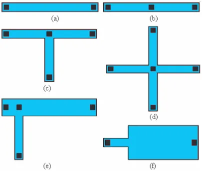
Gan et al. conducted electromigration experiments with Cu dual-damascene tech-nology [10, 39]. The experimental procedure for Cu electromigration was divided into multiple stages: test structure design, sample fabrication, packaging, testing
and failure analyses. Figure 2-1 shows a sample of test structures: straight via-to-via interconnects (‘I’), straight via-to-via-to-via-to-via lines with an additional via-to-via at the center (‘dotted-I’), straight via-to-via lines with an additional metal limb at the center (‘T’), straight via-to-via lines with two additional metal limbs at the center (‘+’), straight via-to-via lines with a transition in width along the interconnect (‘width-transition’) and wider straight via-to-via lines with extra metal limbs nearer to one side of the lines (asymmetrical ‘T’ transition). The test lines are either in the first (M1) or second (M2) level of metallization.
Figure 2-1: Schematic diagrams of designed interconnect trees for electromigration testing (a)‘I’ (b) ‘dotted-I’ (c) ‘T’ (d) ‘+’ (e) asymmetric ‘T’ transition (f ) width-transition.
Test samples were fabricated using a Cu dual-damascene process in IME and SEMATECH. Sixteen samples of each test structure were stressed in a package-level electromigration test system with a temperature range between 50oC and 400oC.
To reduce the possibility of temperature-induced failures and variation in diffusivity due to joule heating, current densities were chosen to limit joule heating below 10oC
through out the experiments. The range of current density in the test structures was between 0.5 to 5.0 M A/cm2
In addition to recording median-time-to-failure (t50) (defined as time to 30%
in-crease in resistance), resistance trends were observed for different structures. Various failure analysis tools, such as Optical Microscopy, SEM, FIB and TEM, were used to characterize the type of failure modes. In the experiments, all failures detected were due to open-circuit failure from formation of voids in a line or via. Experimental results and failure characteristics are presented in detail in [39, 40, 41, 42].
2.2
Via Asymmetric Failure Characteristics in
Cop-per Technology
In Cu interconnects, it has been widely reported that the Cu/Si3N4 interface acts
both as the dominant diffusion pathway for atoms and as the likely site for void nucleation. Due to this fact, the lifetimes of M1 type interconnects are different from that of M2 type interconnects [40]. Gan et al. experimentally demonstrated that the lifetimes of the M2 test structures were always higher than those of the M1 test structures, provided that both types of interconnects had the same length, width, and number of vias at each end. The underlying phenomenon applies to all metal layers and can be generalized using via-above and via-below definitions. The via-above test structures refer to interconnect segments which lie in the first level of metallization, and the vias are located above the test lines. Conversely, the via-below test structures are in the second metallization level while the vias are located below the test lines (see figure 2-2).
During electromigration in Cu interconnects, a tensile stress develops at the cath-ode end, where the T a liner underneath a via forms a blocking boundary to the diffusing Cu atoms. For current Cu technology, the critical tensile stress for void nucleation has been estimated to be 41 M P a or less [43]. In via-below structures, voids preferentially nucleate at the Cu/Si3N4 interface due to the low critical stress
required for that interface. An open-circuit failure would occur only when the void grows to span the whole thickness of the metal line, resulting in a very large void
Figure 2-2: Side-view schematic of void formation in via-above and via-below inter-connects. (a) A small-volume fatal void in via-above interconnects; (b) A large-volume partially-spanning non-fatal void in via-below interconnects.
volume as shown in figure 2-2(b). On the other hand, in via-above structures the maximum tensile stress develops at the Cu/Si3N4 interface near the cathode via.
Therefore, an open-circuit failure would occur if a small-volume void forms below the via, such that the pathway for electron flow is blocked (see Figure 2-2(a)).
This asymmetry in the void volume required for failure not only accounts for the asymmetry in lifetime but also contributes to the different (jL)crit products in
immortality conditions for via-above and via-below type of interconnects. The (jL)crit
values are directly related to the critical stresses required for interconnect failure. The values are reported by Ho et al. to be 3700 A/cm for via-below [44, 45], and by Hau-Riege to be 2100 A/cm for via-above type interconnects [43]. Therefore, in Cu metallization technology, if the electrons are flowing into the line from a via on top, a shorter lifetime and a smaller (jL)crit is expected compared to the condition in which
2.3
Steps in Hierarchical Reliability Analysis for
Copper Metallization
The hierarchical reliability analysis is based on extracting interconnect trees, the fundamental reliability units; applying various stages of filtering conditions to identify mortal units; and then applying a default model to estimate lifetimes of the mortal units. The input to this flow is a circuit layout with mask definitions. The steps for hierarchical reliability analysis in Cu metallization technology are as follows.
(i) Extract interconnect trees from a layout: As defined in section 1.3, an in-terconnect tree is a unit of continuously connected high-conductivity metal lying within one layer of metallization. In addition to geometric properties, the lo-cations of the vias/contacts are also identified in each interconnect tree. Given an interconnect tree in Cu metallization, every via is classified as either “via-above” or “via-below” depending on whether it is located above or below the interconnect line, respectively.
(ii) Determine the longest terminating via-to-via distance, Lmax: When an
in-terconnect tree is constructed from multiple segments as shown in figure 2-3, multiple terminating vias exist due to vias at the end of each segment. To find the longest distance between two terminating vias in an extracted tree, an in-terconnected graph needs to be created where vias and via-to-via distances are represented as nodes and edges, respectively. The shortest path between the vias are calculated using the Minimum Spanning Tree algorithm [46]. Then ter-minating via-to-via distances are just the addition of via-to-via distances along the path. Lmax is chosen to be the longest terminating via-to-via distance.
(iii) Filter interconnect trees using via-above (jL)crit nuc failure criterion: The
first step of the filtering algorithm assumes the worst case scenario. The maxi-mum current density allowed by the design rule, jmax, can be obtained from the
International Technology Roadmap for Semiconductors [2]. Using the worst case threshold of (jL)crit nuc = 1500A/cm [47] (i.e. the via is above the line at the
Lmax
Figure 2-3: Calculating Lmax in an interconnect tree.
cathode end as in a M1 test structure), it is checked whether (jL)crit nuc/jmax >
Lmax for every interconnect tree. If the inequality is true, the tree is considered
immortal and is ignored during further analysis.
(iv) Filter mortal trees using via-below (jL)crit sat failure criterion: Determine
if either of the vias contributing to Lmax is a via-above. If at least one of the vias
happens to be via-above, then the interconnect tree may fail with a via-above (jL)crit nucfailure criterion as determined in the previous step and the
hierarchi-cal flow proceeds directly to step (v). However, if both of the vias are via-below, the via-below (jL)crit sat failure criterion of (jL)crit sat = 3700A/cm [44, 45] is
applied. The condition (jL)crit sat/jmax> Lmax is checked for such interconnect
trees. However, even if a tree passes this test, all the other vias in the tree must be considered before classifying it as immortal. This is because via-above nodes have a much smaller immortality value and thus shorter lengths may fail. The longest distance in the graph from any via-above node to all other vias, Lmax va,
is determined. We again apply the test (jL)crit nuc/jmax > Lmax vato determine
whether the tree might fail.
(v) Estimate the current density, ji, in each segment: The Vdd and Gnd lines
in the circuit layout need to be identified as they have unidirectional current flow and are most susceptible to electromigration failure. Most local interconnects transmit signals between devices in the form of bidirectional or alternating
cur-rent (AC). In these cases, an equivalent direct curcur-rent (DC) which produces the same electromigration damage [48], such as the root-mean-square (RMS) of the AC, is assumed. On the other hand, clock signals usually operate with pulsed DC. Experiments [48] and modeling [49] have shown that the equivalent DC is given by the average of the pulsed DC, Iavg, which is given by the expression
Iavg = rI = Ã ton ton+ tof f ! I (2.1)
where I is the current during the “on” time and r is the duty ratio given by ton
and tof f where tonis the pulse width and the sum of tonand tof f equals the clock
period. The worst case loading of Vdd and Gnd lines can be identified using power consumption reports from a circuit simulation tool. However, estimating current flow at each segment in local interconnects is complicated and requires detailed circuit-level simulation.
(vi) Filter mortal trees by detailed calculation of steady-state stresses: The concept of steady-state stresses in interconnect trees is an extension of the im-mortality condition in stud-to-stud straight lines. The maximum stress differ-ence in an interconnect tree, ∆σmax, is given by the path that has the highest
sum of the (jL) products, summing over the limbs/segments in the path [18]. This is expressed by ∆σmax = ρeZ∗ Ω (jL)ef f (2.2) where (jL)ef f = max all junction pairs i, j
à X k jkLk ! (2.3) where ∆σmax is the stress difference between the anode and the cathode, Z
∗
is the effective charge number, e is the elementary charge, ρ is the electrical resistivity of the metal, Ω is the atomic volume, i and j are two terminating vias, and jk and Lk are the current density in, and length of, segment k along
the path between i and j, respectively. To filter the immune interconnect trees using (jL)ef f, repeat steps (iii) and (iv) by replacing (jL)max with (jL)ef f.
(vii) Analyze mortal trees with electromigration failure models: A conserva-tive default electromigration model based on the analysis of individual nodes (vias or contacts) in a tree is used to estimate the lifetime of a mortal tree. The output of the model is taken to be the median-time-to-failure of a tree. The default model is discussed in a later section. Furthermore, numerical methods can be applied for detailed calculation of the time-dependent stress analysis. Software programs, such as MIT/EmSim [9, 50] and CuEmSim [51] , allow the calculation of stress evolution in multi-terminal interconnect trees.
(viii) Apply full chip stochastic reliability model: The median-time-to-failure (MTTF) or t50 of each mortal interconnect tree is estimated using the
de-fault model or a micro-structure level electromigration simulation program (e.g. MIT/EmSim). The full-chip reliability model combines the t50of multiple
inter-connect trees from the same layout and provides a set of reliability metrics for the overall chip. The stochastic model and underlying reliability mathematics are discussed in the next chapter.
2.4
Contrast with Hierarchical Reliability
Analy-sis in Aluminum Metallization
Failure mechanisms in Cu and Al interconnects are significantly different due to their different architectural schemes as described in section 1.2. In Al metallization structures, the Al line has refractory metal layers above and below, and tungsten (W ) filled vias are used to connect interconnects from different levels. The W -filled vias act as a perfect and symmetric diffusion barrier irrespective of the electron flow direction. Therefore, lifetime differences were not observed for M1 and M2 type structures in Al metallization.
Via classification is not required in hierarchical analysis flow for Al technology. Steps (iii) and (iv) in the hierarchical reliability analysis are merged into one where a single (jL) product threshold, (jL)sat = 4000A/cm, is applied to check for