HAL Id: hal-01900747
https://hal.archives-ouvertes.fr/hal-01900747
Submitted on 29 Jul 2020
HAL is a multi-disciplinary open access
archive for the deposit and dissemination of
sci-entific research documents, whether they are
pub-lished or not. The documents may come from
teaching and research institutions in France or
abroad, or from public or private research centers.
L’archive ouverte pluridisciplinaire HAL, est
destinée au dépôt et à la diffusion de documents
scientifiques de niveau recherche, publiés ou non,
émanant des établissements d’enseignement et de
recherche français ou étrangers, des laboratoires
publics ou privés.
Impact of CMOS Post Nitridation Annealing on
Reliability of 40nm 512kB Embedded Flash Array
Thibault Kempf, Marc Mantelli, François Maugain, Arnaud Regnier,
Jean-Michel Portal, Pascal Masson, Jean-Michel Moragues, Marjorie Hesse, V.
Della Marca, Julien Franck, et al.
To cite this version:
Thibault Kempf, Marc Mantelli, François Maugain, Arnaud Regnier, Jean-Michel Portal, et al..
Im-pact of CMOS Post Nitridation Annealing on Reliability of 40nm 512kB Embedded Flash Array. 2017
IEEE International Integrated Reliability Workshop (IIRW), Oct 2017, Fallen Leaf Lake, CA, United
States. �hal-01900747�
Impact of CMOS Post Nitridation Annealing on
Reliability of 40nm 512kB Embedded Flash Array
Thibault Kempf
1,2,3, Marc Mantelli
1, François Maugain
1, Arnaud Regnier
1, Jean-Michel Portal
2, Pascal Masson
3,
Jean-Michel Moragues
1, Marjorie Hesse
1,3, Vincenzo della Marca
2, Franck Julien
1, Stephan Niel
1 1STMicroelectronics, Rousset, France 2
IM2NP, Aix-Marseille University, Marseille, France 3
EpOC / Nice Sophia-Antipolis University, Biot, France
Abstract—The impact of CMOS post nitridation annealing
(PNA) temperature on a 40nm embedded Flash reliability is studied. Electrical characterizations of the Flash tunnel oxide are carried out on single cell. These are used to explain the better results in terms of endurance and data retention obtained on a 512kB test chip with a lower annealing temperature. This result can be linked with the decrease of nitrogen in the bulk oxide, improving oxide wear out performance against electrical stress and stress induced leakage current (SILC). The on-chip characterization is, here, an invaluable tool to show the extrinsic behavior in the memory array and apply product-like stress.
Keywords—40nm Flash NOR; embedded process; circuit testing; nitrided oxide; fixed charge; oxide wearout; data retention; endurance; on-chip characterization
I. INTRODUCTION
Embedded Flash memories down-scaling is only possible with the optimization of logic and high voltage devices together with the memory cell. One optimization path is the introduction of nitrided oxide to enhance the oxide robustness versus electrical stress and to reduce dopant inter-diffusion [1][2]. Previous studies have shown the importance of the nitrogen distribution in the tunnel oxide and the relationship between process temperature and nitrogen bonding [3][7].
While CMOS oxide requires a large nitrogen dose and annealing to heal the defects generated by previous nitridation [8] [9], memory oxide is more complex to optimize in order to ensure the upkeep of dielectric properties such as the lowest possible EOT (Electrical Oxide Thickness), a good boron dopant diffusion barrier but, as well, a good reliability in terms of cycling and retention. Thus both interface and bulk oxide should be optimized to be resistant to charge injection through the oxide during the programing and erasing operation. From [3][7], it is assumed that nitrogen should be located at the oxide interfaces to create Si-N stronger bonds preventing degradation by Fowler-Nordheim (FN) and channel hot electron (CHE) stress[10]. Moreover it is also shown that too high a nitrogen concentration in the bulk oxide can have a negative impact due to Si-N bonds distorted by the lattice difference between SiO2 and Si3N4 [12]. In this case performance in cycling is known to decrease due to the field-induced generation of fixed negative oxide traps decreasing programing or erasing efficiency. Stress induced leakage current (SILC) is also linked to nitrogen dose
in the oxide from [10], and [4] proves that too high a N dose in the bulk oxide can generate different kinds of traps leading to the creation of a conductive path and thus to SILC mechanisms during retention.
Development of the nitridation process has thus focused on proposing a way to insert nitrogen at a specific location in the oxide thickness. While decoupled plasma nitridation (DPN) targets top nitridation, thermal annealing under NO, NO2 or NH3 (like in [13][5]) can lead to localization of nitrogen at the oxide channel interface. The annealing process after nitridation aims to modify nitrogen bonding after a specific nitridation method [8] and to heal defects generated by high dose oxide nitridation (such as DPN). The consequence is the redistribution of nitrogen in the oxide as in [12].
In this context, the aim of this paper is to study the impact of logic post nitridation annealing (PNA) temperature on 40nm 512kB embedded Flash array reliability. Firstly single device structures, such as capacitive test elements or single memory cells, are used to study tunnel oxide properties’ evolution with PNA temperature at initial state and after degradation. Then on-chip characterization setups are presented and their results used to validate the evolution on memory reliability with the PNA temperature. Finally we discuss the correlation between PNA temperature, nitrogen profile and gain on Flash reliability for this technology.
II. EMBEDDED NORFLASH PROCESS
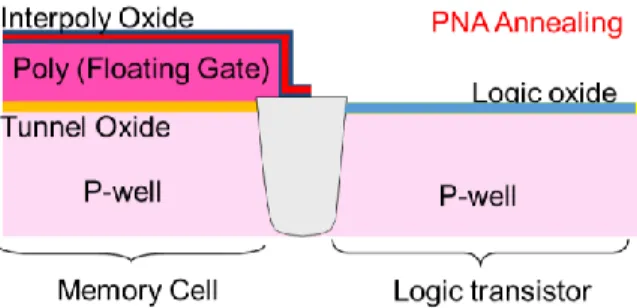
In an embedded Flash process, a typical self-aligned polysilicon Flash stack is first processed as follow: (1) Tunnel oxide annealing in N2O, (2) polysilicon phosphorous doping and (3) inter-poly deposition above. Then core logic oxides
are grown and nitrided by decoupled plasma nitridation (DPN). To heal the defects generated by DPN and in order to optimize the nitrogen incorporation in the oxide, a final PNA is applied as described Fig. 1. Thus both oxides (tunnel and core logic) are affected by the PNA step. In order to limit the impact of the PNA on tunnel oxide, a lower temperature (Low PNA) is used (decreased by 5% compared to POR temperature). The experimental results of the comparison between the process of reference (POR) and the Low PNA temperature process (Low PNA) are thus presented in this paper.
III. EXPERIMENTAL RESULTS
A. Device description for single device characterization Single device measurements are done in 40nm technology node. Capacitance Voltage (CV) measurements are obtained on tunnel oxide capacitor plates on active area (of 1x10⁻³cm²). Charge pumping (CP) characterization and constant voltage stress (CVS) interrupted by CV are realized on large transistors (WxL=10mx10m) with tunnel oxide. Single memory cell measurements are realized on our Flash NOR cells programed by Channel Hot Electron (CHE) and erased by Fowler-Nordheim (FN) mechanism.
B. Study of logic PNA temperature impact on capacitive structure
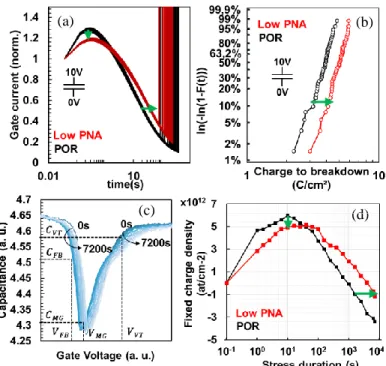
The electrical characterization of tunnel oxide capacitors was carried out. Measured gate currents of fresh devices, in Fig.(a) and (b), show that both, Low PNA and POR, give similar performance in electron injection while EOT measurements from CV in accumulation (not shown) are also aligned. However the Low PNA presents a larger density of interface states compared to POR (Fig.(c) and (d)) which is inherent to a lower interface healing or lower nitrogen diffusion as reported in [1].
As described in Fig. 3 (a), the degradation of tunnel oxide under CVS is indicative of a difference in degradation between POR and Low PNA. The most important increasing of gate current for POR at the beginning of CVS results in a larger positive trapping. Then, after 1s stress a faster negative
trapping is observed for the POR, and causes the gate current decreasing respect to the Low PNA, with a consequent increasing of the time to breakdown. Indeed the time to breakdown at 63% (TBD63%) is lower and less spread for Low PNA (200s) compared to POR (272s). In Fig. 3 (b) the extraction of the charge to breakdown (QBD) is reported. In the case of Low PNA the QBDincreases because of the smaller negative charge trapping that involves in a higher gate current and thus a faster breakdown, in according with the CVS results. However the tunnel oxide breakdown it is not considered as an issue for Flash memory [7], while the most important reliability parameter to consider is the quantity of fixed charge trapping.
To confirm these results, constant voltage stress interrupted by capacitance voltage characterization is presented in Fig. 3 (c). Using the method in [14], the mean interface states and mean fixed charge oxide densities are extracted. The same dynamic of interface state generation is observed for the two splits (not shown here). However the fixed charge generation,
described in Fig. 3 (d), presents the same evolution of CVS (d)
(b) (a)
(c)
Fig. 2. Oxide characterization at fresh state for Low PNA (red) and POR (black): Gate current measured on oxide capacitive structure for positive bias (a) and negative bias (b). 2-level charge pumping characterization (c). Interface states densities extraction (d) from multi-frequencies sinusoidal 2-level charge pumping method.
Fig. 2.Write and erased linear threshold voltage (a) and transconductance (b) for 18 dice at fresh state.
(a) (a)
(b)
Fig. 3. (a) Constant Voltage Stress (CVS) and (b) Charge to breakdown on 50 dice on capacitive structure in inversion at 125°C. (c) Constant voltage stress on capacitive structure interrupted by Capacitance Voltage (CV) measure from fresh state (dark blue) to 7200s of stress (light blue). (d) Fixed charge mean density extracted from CV.
(a) (a) (b) (b) (c) (c) (d) (d)
characteristics, finally indicating a larger and faster degradation of POR oxide.
C. Focus on logic and high voltage transistors properties In order to verify the functioning of logic and high voltage transistors, we reported in Fig. 4 the threshold voltages of NMOS and PMOS used in the test chip of memory array. We notice that in both cases this parameter is not impacted by the lower PNA temperature process. The impact of PNA temperature on the transistor performances is acceptable compared to required specifications and qualification criteria for this technology.
D. Single memory cell characterization and cycling
As shown before we obtain the same injection performance for both process oxide stacks. Hence, the threshold voltages of memory cells are well aligned at the initial state in Fig. 55 (a). Even if the density of interface states is larger for low PNA in the fresh state, the transconductance for both splits is identical, in Fig. 55 (b). We thus demonstrate that the interface states density is too low to affect reading characteristics in the fresh state.
We carried out a series of endurance experiments (18 dice) on single cell memory. In Fig. 6, the erase efficiency degradation is plotted, we highlighted a lower threshold voltage shift (300mV less) for Low PNA that grants a slightly increased programing window (PW) at the end of cycling. As explained in [5], the gain in terms of endurance is due to the slight generation of negative fixed charges in the Low PNA tunnel oxide. However to confirm these results, on-chip
characterizations are performed to obtain larger statistic and a product-like approach.
E. Test conditions for on-chip characterizations
Our test chip, described in Fig. 7(a), is a 512kB microcontroller unit with the previously studied 40nm technology node Flash organized in two NOR arrays. It is also composed of high voltage and logic circuits in order to: access, program, erase and read the memory as in a final product. In addition, four specific test functions are available: (i) direct memory access (DMA), (ii) built-in-self-test (BIST), (iii) threshold voltage distribution using an external voltage source, (iv) internal generated biases monitoring.
Test. Number of testchip x Memory size Cycling Conditions Test sequence Erase algo. T (°C) Cycling VT Verify and retention A 8x16KB No 25°C 500k Erase+CKB+CKI No B 40x16KB Yes 25°C and 105°C 500k Erase+CKB+CKI Yes C 40x16KB 500k Erase + CKB D 40x16KB 100k Erase+CKB+CKI With relaxation Table 1 (a) (a) (b) (b) (c) (c)
Fig. 3. (a) 512kB NOR memory MCU testchip with implemented reliability test functions. (b) Erase pulses increasing in amplitude and number with cycle number to
emulate an erase algorithms on the product. (c) Statistical parameter extraction from threshold voltage distribution: average (μ), average +/- 2 standard deviation (σ) and extrapolation of distribution tail to reading voltage to evaluate technology defectivity
Fig. 4. Erase threshold voltage shift of 18 dice during cycling using normal programing by CHE and erasing by FN conditions.
Fig. 5. Threshold voltage for (PMOS and NMOS) logic (a) and high voltage transistors (b). Low and high specification limits (dotted lines) are indicative of process quality.
All the studied units have passed the electrical wafer sorting (EWS) and so conform to required specifications. The EWS allows to screen different kinds of defects: short term memory or test chip failure, such as metal lines short/open, contact to gate, fast erase bits and fail bits. Moreover, in order to maintain the initial programming window constant for each
test chip, it is possible to trim: the bandgap, the reference current as well as the control gate programing and erasing voltages.
Table 1 describes the four experiments presented here. A constant voltage condition is applied for cycling in A test, while experiments B, C and D use cycling with erase algorithms to reproduce product-like stress. The erase phase is performed increasing the number of pulses and the amplitude as shown in Fig. 7(b).They are initially fixed to validate an approximate constant programing window during the whole cycling for this given technology. By this means, the electrical stress equivalent to the one applied on a product (with an erase algorithm implemented) is used. In A, B and D the cycling sequence is composed by a global erase step, followed by two programing operations with a checkerboard and inverse checkerboard pattern (resp. CKB and CKI). However CKI pattern programing step is skipped for test C in order to obtain the half of memory array stressed only by the erase operation. Tests B, C and D are repeated at 25°C and 105°C, and the available memory array is partitioned in such a way as to realize them in parallel and on the same units. Moreover the relaxation is just applied during the test D with a duty cycle of 20%. For retention tests, the whole memory is reconditioned using programing and erasing verify algorithms. Test chips are then baked at 150°C for up to 2000h interrupted by a readout step at 48h, 168h, 500h, 1000h, and 2000h.
In Fig. 7 (c), defectivity is extrapolated from the cumulated distribution with an exponential fit at the reading voltage. It gives a normalized criterion of the amount of failed cells (0.1ppm fail equivalent to 1 cell fail every 10M). The average and 4 times standard deviation window (to monitor 95.6% of cell distribution) is also used.
F. Testchip cycling with product-like test
First, Fig. 8 presents the result of experiment A. A weaker erased threshold voltage degradation is observed on the Low
PNA with respect to the POR test chips. This validates the previous results on single devices and confirms, with larger statistic, the gain on cycling for Low PNA with a programing
window closure reduced by 10%. Moreover standard deviation shows that the shift is intrinsic with the same dispersion.
Experiments B and D show the results of cycling with erase algorithms summarized inTable 2. Low PNA yields a lower defectivity whatever the cycling test and temperature. It confirms the gain on cycling for the Low PNA process with product-like stress. In Fig. 9, we observe that the gain on cycling at 105°C (Fig. 9(b)) is reduced compared to ambient temperature cycling (Fig. 9(a)). It can be explained by a partial detrapping of negative fixed charge at 105°C which reduces the difference in degradation between POR and Low PNA. The results of experiment C are not reported because the over-erased cells are localized out of the characterization voltage window (used to reduce gate stress during readout).
G. Post-cycling retention on testchip
Regarding the extrinsic cells, from retention results of experiment B described in Fig. 10, a slightly lower number of
Test
Defectivity at reading voltage for erased cells after cycling
25°C 105°C
POR Low PNA POR Low PNA
B 4.6x10⁻⁸ 1.5x10⁻⁹ 1.98x10⁻⁶ 1.07x10⁻⁷
D 1.7x10⁻¹⁰ 4.2x10⁻¹¹ 2.8x10⁻¹⁰ 1.4x10⁻¹²
Fig. 7. Erase threshold voltage evolution of 1 million memory cells over 16 testchips during 500k cycling test with constant voltage conditions, average and 4 standard deviation window describe the threshold voltage distribution shift
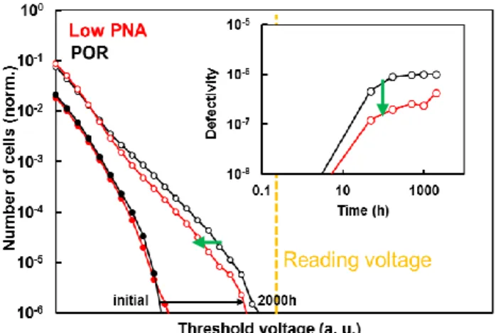
Fig. 8. Threshold voltage distribution of erased cell cycled at 25°C and up to 500k after reconditioning and after 2000h retention at 150°C (test B). Inset shows defectivity at reading voltage during retention of test B.
Fig. 6. Threshold voltage distribution for experiment B after 500k cycle at 25°C (a) and 105°C (b) and a special reconditioning with default erase conditions. Direct evaluation of erase efficiency degradation is done by the shift of threshold voltage between POR and Low PNA.
(a) 25°C (b) 105°C
cells are subject to SILC for Low PNA and this creates smaller extrinsic tails out of the threshold voltage distribution. Indeed, POR shows extrinsic bits as traps are present in higher numbers in the bulk oxide. Thus, it results, more likely, in a conductive path formation, based on the assumption that SILC is partially governed by the uniform distribution traps density in the tunnel oxide [3].
Furthermore, few extrinsic cells are observed for the programmed state which suggest an asymmetry of trapping in the tunnel oxide of SILC-related traps. Given that interface states and near interface traps also play a role in SILC mechanism, the anode hole injection (AHI) mechanism, related to the erase operation, can explain this asymmetry of extrinsic tails. Hot holes are trapped in the tunnel oxide near the channel during the erasing operation only. The largest extrinsic tails are visible for test D in Fig. 11 (a). Drain disturb may happen during the relaxation period as other sectors of the Flash test chips are cycled. This may induce a different degradation of tunnel oxide by injecting hot holes generated by band to band mechanism. Hence, the number of extrinsic cells for written distribution is increased.
We do not see any impact on retention for Low PNA programed cells (Fig. 11 (a) and (b)) except for test C as described in Fig. 11 (c). The over-erase stress (added to the gate stress due to programing of neighboring cells) highlights the difference of the two studied process steps, in terms of oxide reliability during retention. The POR defectivity increases faster compared to Low PNA defectivity in Fig. 11 (c) for the same cycling temperature. This suggests that another charge loss mechanism is added to the main retention behavior of this Flash. As demonstrated above, the POR oxide traps a higher number of electrons, thus the detrapping of these charges can decrease the globally negative charge of programed cells, lowering threshold voltage.
IV. DISCUSSION
The effect of PNA temperature on nitrogen profile is shown on SIMS characteristics in Fig. 12. Firstly, the redistribution of nitrogen in the whole oxide is lower for Low PNA. It reaches an intermediate state between no annealing step and the process of reference. Secondly, considering that the annealing partially heals nitrogen dose at oxide/channel interface, for the Low PNA the temperature reduction limits the relaxation of strain at the tunnel oxide interface.
The first assumption is verified by single-device oxide degradation and testchip cycling. Increasing nitrogen dose in the bulk oxide the oxide reliability is decreased in terms of cycling due to a faster generation of negative fixed charges in this the tunnel region. This faster oxide charging is due to an excessive number of nitrogen links that distorts SiO2 bonding network creating strained bonds. These are easily broken under electric stress. Moreover CVS and retention test results show respectively a larger positive trapping and a higher sensitivity to SILC for POR. The POR oxide may trap more positive charges, which generates this current increasing on CVS and results in a higher probability of obtaining leakage paths through the tunnel oxide.
The second assumption is proved by the harmless increase of interface states in the fresh devices characterized by CP. It highlights a potential limit of PNA temperature decrease. Too low a temperature may lead to a less-effective healing of the memory oxide interface.
V. CONCLUSION
In this paper, the direct correlation between nitrogen profile in tunnel oxide and the Flash endurance and retention has been verified on a 512kB test chip. We show the impact of PNA temperature on CVS and QBD characteristics. The extraction of fixed charge density is a main parameter to control the oxide reliability in a 40nm embedded Flash process. The electrical characterizations on single devices and test chips have demonstrated that avoiding the nitrogen redistribution in the
Fig. 10. Effect of Post Nitridation Annealing (PNA) temperature on nitrogen diffusion in tunnel oxide studied by SIMS on similar interpoly/polySi/TO stack. DPN without PNA nitrogen profile is a reference for nitrogen profile evolution. However this process is not applicable for electrical characterization as core logic and high voltage voltage are not functional in this case.
(a) (b) (c)
Fig. 9. (a) Written cells of test D before and after bake showing the largest amount of extrinsic cells for written cells. (b) describes defectivity of test B test chips for written cells. (c) describes defectivity of test C test chips for written cells. The slope of the power function fitting the defectivity characteristics is indicated at the left of each curves.
TEST D
TEST B
TEST C
Reading voltage
bulk of tunnel oxide the cell endurance increases, while the sensibility to SILC mechanism during post-cycling retention is limited. Finally this CMOS process step enables to achieve a better defectivity on the test chip. This has been demonstrated by different types of endurance and retention experiments on 4MB of 40nm embedded Flash. This improvement on memory technology can be done without impact on core logic or high voltage devices.
REFERENCES
[1] K. Takasaki, K. Irino, T. Aoyama and T. Ito , "Impact of nitrogen profile in gate nitrided-oxide on deep-submicron CMOS performance and reliability," in , vol.39, no., pp., Jan. 2003.
[2] D Brazzelli; G Ghidini; B Crivelli; R Zonca; M Bersani, "High quality thin oxynitride by RTP annealing of in situ steam generation oxides for flash memory applications ," in Solid-State Electronics , vol.45, no.8, pp.1271 - 1278, 2001.
[3] T. Kim, S. Koka, S. Surthi and K. Zhuang, " Direct Impact of Chemical Bonding of Oxynitride on Boron Penetration and Electrical Oxide Hardening for Nanoscale Flash Memory ," in IEEE Electron Device Letters, vol.34, no.3, pp.405-407, Mar. 2013.
[4] T. Kim, K. Sarpatwari, S. Koka and H. Wang, "Comprehensive Understanding on the Role of Tunnel Oxide Top Nitridation for the Reliability of Nanoscale Flash Memory," in IEEE Electron Device Letters, vol.34, no.3, pp.396-398, Mar. 2013.
[5] U. Ganguly, et al., "Impact of Top-Surface Tunnel-Oxide Nitridation on Flash Memory Performance and Reliability," in IEEE Electron Device Letters, vol.31, no.2, pp.123-125, Feb. 2010.
[6] W. H. Lee, et al., "Post-cycling data retention failure in multilevel nor flash memory with nitrided tunnel-oxide," in 2009 IEEE International Reliability Physics Symposium, pp.907-908, Apr. 2009.
[7] G. Ghidini; D. Brazzelli; C. Clementi; F. Pellizzer, "Charge trapping mechanism under dynamic stress and its effect on failure time [gate oxides]," in 1999 IEEE International Reliability Physics Symposium Proceedings. 37th Annual (Cat. No.99CH36296), vol., no., pp.88-92, 1999.
[8] F.N. Cubaynes, J. Schmitz, C. Van Der Marel, J.H.M. Snijders, A. Veloso, A. Rothschild, C. Olsen; L. Date, " Symposium on silicon nitride and silicon dioxide thin insulating films," May. 2003.
[9] M. Bhat; D. J. Wristers; Liang-Kai Han; Jiang Yan; H. J. Fulford; Dim-Lee Kwong, "Electrical properties and reliability of MOSFET's with rapid thermal NO-nitrided SiO2 gate dielectrics," May. 1995.
[10] Chao Sung Lai; Tan Fu Lei; Chung Len Lee, "The electrical characteristics of polysilicon oxide grown in pure N/sub 2/O," in IEEE Electron Device Letters, vol.16, no.9, pp.385-386, Sep. 1995.
[11] J. De Blauwe; R. Degraeve; R. Bellens; J. Van Houdt; P. Roussel; G. Groeseneken; H. E. Maes, "Study of DC Stress Induced Leakage Current (SILC) and its Dependence on Oxide Nitridation," Sep. 1996.
[12] Yue Xu; Yang Huang, "Influence of ISSG tunnel oxide with decoupled plasma nitridation on erase characteristic of NOR-type floating-gate flash memories," Jun. 2015.
[13] T. Guarini et al., "Nitric oxide rapid thermal nitridation for Flash memory applications," 2010 18th International Conference on Advanced Thermal Processing of Semiconductors (RTP), Gainesville, FL, 2010, pp. 166-170. [14] M. Carmona; L. Lopez; J. L. Ogier; D. Goguenheim, "Degradation mechanism during gate stress at high electrical field on high voltage MOSFET for non-volatile memory applications," in 2014 IEEE International Integrated Reliability Workshop Final Report (IIRW), vol., no., pp.147-150, Oct. 2014.