HAL Id: inserm-02430395
https://www.hal.inserm.fr/inserm-02430395
Submitted on 9 Jan 2020
HAL is a multi-disciplinary open access
archive for the deposit and dissemination of
sci-entific research documents, whether they are
pub-lished or not. The documents may come from
teaching and research institutions in France or
abroad, or from public or private research centers.
L’archive ouverte pluridisciplinaire HAL, est
destinée au dépôt et à la diffusion de documents
scientifiques de niveau recherche, publiés ou non,
émanant des établissements d’enseignement et de
recherche français ou étrangers, des laboratoires
publics ou privés.
Optimized 3D metasurface for maximum light deflection
at visible range
Mahmoud M. R. Elsawy, Stéphane Lanteri, Régis Duvigneau, Gauthier Brière,
Patrice Genevet
To cite this version:
Mahmoud M. R. Elsawy, Stéphane Lanteri, Régis Duvigneau, Gauthier Brière, Patrice Genevet.
Op-timized 3D metasurface for maximum light deflection at visible range. META 2019 - 10th
Interna-tional Conference on Metamaterials, Photonic Crystals and Plasmonics, Jul 2019, Lisbonne, Portugal.
�inserm-02430395�
META 2019, LISBON - PORTUGAL, JULY 23 – 26, 2019
Optimized 3D metasurface for maximum light deflection at visible range
Mahmoud M. R. Elsawy
1∗, St´ephane Lanteri
1, R´egis Duvigneau
1,
Peinan Ni
2, Gauthier Bri`ere
2, and Patrice Genevet
2 1INRIA, 06902 Sophia Antipolis Cedex, France2CNRS, CRHEA, Universit´e Cˆote d’Azur, rue Bernard Gregory, Sophia Antipolis, Valbonne, France
*corresponding author, E-mail: [email protected]
Abstract
In this contribution, we use two different efficient global optimization techniques in order to optimize 3D real life gradient metasurface based on GaN semiconductor. Our results show that we can achieve more than 87% of diffrac-tion efficiency at the visible regime using only 150 solver calls for optimizing 12 parameters. Our methods seem to be more efficient than other optimization techniques that re-quire costly simulations, especially for 3D structures. The optimized structure will be fabricated and characterized ex-perimentally.
1. Introduction
The field of metasurface has drawn a lot of attention in the last few years, because of the offered degrees of free-dom that provide nearly a full control of the light proper-ties in a very short propagation distance with high resolu-tion [1, 2, 3]. The complexity of the problem, the wide parameter space, and the new fabrication capabilities, make the direct modelling problem insufficient and the use of in-verse design is mandatory to achieve the maximum desired performance [4]. Several optimization methodologies have been used in the field of metasurfaces, including local and global search methods. The former, require fewer itera-tions, however, they can be stuck in local maxima/minima, the later is more general and is suitable for optimizing large parameter space. Nevertheless, most of the global tech-niques used in the metasurface designs require large num-ber of solver calls, which make them inapplicable for mod-elling 3D real-life designs that require 3D solvers. The main target of this contribution is to find an optimal geom-etry for 3D gradient metasurface made of GaN nano-ridges (see the inset in Fig. 1) in order to achieve a maximum light deflection (in the same plane of incidence) with a specific angle at λ = 600 nm. We choose GaN semiconductor due to its negligible losses and due to its high refractive index in the visible regime, which make it ideal nanoresonator (phase-shifters) for metasurface designs [1, 3].
Here, we use two different efficient global optimization techniques based respectively on advanced evolution strate-gies and statistical learning. The first one is the covariance matrix adaptation evolution strategy (CMA-ES) [5]. The CMA-ES has been gaining a lot of attention since it requires fewer cost function evaluations compared to the other
evo-lutionary algorithms like genetic algorithms (GA) [4, 6] especially for 3D designs that require expensive simula-tions. The second method is the Efficient Global Opti-mization (EGO) algorithm [7]. The EGO algorithm is based on the surrogate modelling, that is to say, replac-ing the complex or costly evaluation process by a simpler and cheaper model [7] to reduce dramatically the computa-tional cost (number of calls for the electromagnetic solver). We use our rigorous Discontinuous Galerkin Time Domain (DGTD) solver from the DIOGENES software suite dedi-cated to computational nanophotonics [8] together with the optimization algorithms, in order to achieve a maximum diffraction efficiency (η(n, m), where n, m are the mode indices) at λ = 600 nm. We consider a normal incident
0.10 0.20 0.30 0.40 0.50 0.60 0.70 0.80 0.90 1.00 50 100 150 200 250 1 − η (0, − 1) Solver
DOE for EGO EGO optimization CMA−ES optimization 1500 nm 300 n m x y z calls
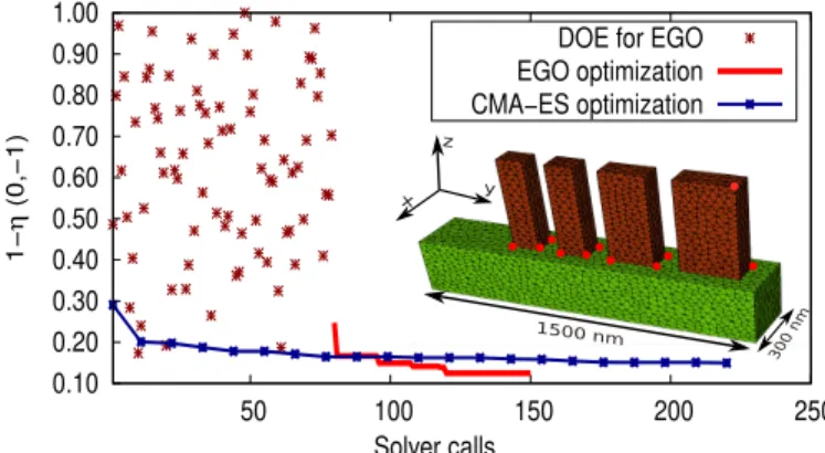
Figure 1: Optimization process using the EGO (red curve) and the CMA-ES (dark blue curve) methods as a function of the solver calls. The dark red points represent the DOE for the EGO. The inset shows the geometry under considera-tion, green region for the substrate (Al2O3), GaN ridges are
shown in red. The 12 red circles represent the optimization parameters.
plane-wave with electric field polarized in the y-direction, and we aim to maximize the diffraction efficiency of the first order mode η(0, −1) (deflect light in the same plane of incidence y-z plane). Thus, we consider a sub-wavelength period in the x-direction (300 nm), and we consider a pe-riod of 1500 nm in the y-direction, as it can be seen in the inset shown in Fig. 1. We restrict ourselves to rectangu-lar shapes made of GaN semiconductor, in which the posi-tion and x and y thicknesses together with the height of the ridges need to be optimized. The 12 optimized parameters
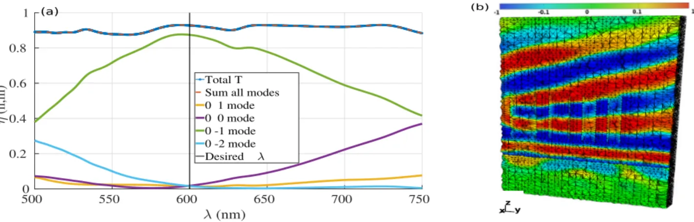
(b) 500 550 600 650 700 750 (nm) 0 0.2 0.4 0.6 0.8 1 (n,m) Total T Sum all modes 0 1 mode 0 0 mode 0 -1 mode 0 -2 mode Desired (a)
Figure 2: (a): Diffraction efficiency η(n, m) for the main modes as a function of the wavelength, the total transmission is shown in blue. (b); <e(Ey) obtained from our DGTD solver [8] at λ = 600nm.
are represented by the red circles in the inset of Fig. 1. In Fig. 1, we show the results obtained using our opti-mization techniques. First, for the EGO model, the dark red points represent the design of experiment (DOE) obtained before the optimization process in the EGO model. Based on these points, a surrogate model is constructed and will be used during the optimization process to find a global mini-mum below the best point found in the DOE process. More precisely, after only 150 iterations (solver calls), we opti-mized 12 parameters and obtained a diffraction efficiency around 87% at λ = 600 nm, which is sufficient for us at least at this moment, since we need to make a compro-mise between the number of iterations and the maximum diffraction efficiency obtained. The diffraction efficiency of the main modes, and total transmission as a function of the wavelength can be obtained in Fig. 2(a). As it can be seen, at λ = 600 nm, nearly all the light is concentrated at the first order mode which is inferred in Fig. 2(b). Second, in Fig. 1, we show the results obtained from CMA-ES (dark blue curve). We have found that after 200 iterations, we ob-tain a point in which the diffraction efficiency is above 85%, but still the EGO provides a better point than the CMA-ES, at least below 200 iterations.
In conclusion, we used our global optimization tech-niques to optimize 3D gradient metasurface. Our results reveal that we can get up to 87% of diffraction efficiency by optimizing 12 different parameters using only 150 it-erations. Our techniques seem to be more efficient than the usual global optimization methods [6] available in the literature in which numerous simulations are required for achieving optimized geometries. Based on the above re-sults, the optimized geometry will be fabricated and charac-terized experimentally using our modern and efficient fab-rication techniques.
References
[1] P. Genevet, F. Capasso, F. Aieta, M. Khorasanine-jad, and R. Devlin, “Recent advances in planar op-tics: from plasmonic to dielectric metasurfaces,” Op-tica, vol. 4, no. 1, pp. 139–152, 2017.
[2] S. Sun, K.-Y. Yang, C.-M. Wang, T.-K. Juan, W. T. Chen, C. Y. Liao, Q. He, S. Xiao, W.-T. Kung, G.-Y. Guo, et al., “High-efficiency broadband anoma-lous reflection by gradient meta-surfaces,” Nano let-ters, vol. 12, no. 12, pp. 6223–6229, 2012.
[3] N. Schmitt, N. Georg, G. Bri`ere, D. Loukrezis, S. H´eron, S. Lanteri, C. Klitis, M. Sorel, U. R¨omer, and P. Genevet, “Optimization and uncertainty quan-tification of gradient index metasurfaces,” Optical ma-terial expressvol. 9, pp. 892–910 (2019)
[4] S. Molesky, Z. Lin, A. Y. Piggott, W. Jin, J. Vuckovic, and A. W. Rodriguez, “Outlook for inverse design in nanophotonics,” arXiv preprint arXiv:1801.06715, 2018.
[5] N. Hansen, S. Muller, and P. Koumoutsakos, “Re-ducing the time complexity of the derandomized evolution strategy with covariance matrix adapta-tion (CMA-ES),” Evoluadapta-tionary Computaadapta-tion, vol. 11, no. 1, pp. 1–18, 2003.
[6] V. Egorov, M. Eitan, and J. Scheuer, “Genetically op-timized all-dielectric metasurfaces,” Optics express, vol. 25, no. 3, pp. 2583–2593, 2017.
[7] D. Jones, “A taxonomy of global optimization meth-ods based on response surfaces,” Journal of Global Optimization, vol. 21, pp. 345–383, 2001.
[8] DIOGENES: A Discontinuous-Galerkin based soft-ware suite for nano-optics. https://diogenes.inria.fr/. [9] Zhenpeng Zhou, Juntao Li, Rongbin Su, Beimeng
Yao, Hanlin Fang, Kezheng Li, Lidan Zhou, Jin Liu, Daan Stellinga, Christopher P Reardon, et al. Efficient silicon metasurfaces for visible light. ACS Photonics, 4(3):544–551, 2017.
[10] David Sell, Jianji Yang, Evan W Wang, Thaibao Phan, Sage Doshay, and Jonathan A Fan. Ultra-high-efficiency anomalous refraction with dielectric meta-surfaces. ACS Photonics, 5(6):2402–2407, 2018. 2