A 36 nW, 7 ppm/°C on-Chip Clock Source Platform
for Near-Human-Body Temperature Applications
The MIT Faculty has made this article openly available.
Please share
how this access benefits you. Your story matters.
Citation
Kamakshi, Divya Akella, Aatmesh Shrivastava, Chuhong Duan,
and Benton H. Calhoun. “A 36 nW, 7 ppm/°C on-Chip Clock Source
Platform for Near-Human-Body Temperature Applications.” JLPEA
6, no. 2 (May 16, 2016): 7.
As Published
http://dx.doi.org/10.3390/jlpea6020007
Publisher
MDPI AG (Basel, Switzerland)
Version
Final published version
Citable link
http://hdl.handle.net/1721.1/105142
Terms of Use
Creative Commons Attribution 4.0 International License
Low Power Electronics and Applications
Article
A 36 nW, 7 ppm/
˝
C on-Chip Clock Source Platform for
Near-Human-Body Temperature Applications
Divya Akella Kamakshi1,*, Aatmesh Shrivastava2, Chuhong Duan3and Benton H. Calhoun1
1 Department of Electrical and Computer Engineering, University of Virginia, Charlottesville, VA 22904, USA;
2 PsiKick Inc. Charlottesville, VA 22902, USA; [email protected]
3 Electrical Engineering and Computer Science Department, Massachusetts Institute of Technology,
Cambridge, MA 02139, USA; [email protected]
* Correspondence: [email protected]; Tel.: +1-434-243-2076 Academic Editor: Alexander Fish
Received: 4 February 2016; Accepted: 5 May 2016; Published: 16 May 2016
Abstract:We propose a fully on-chip clock-source system in which an ultra-low-power diode-based temperature-uncompensated oscillator (OSCdiode) serves as the main clock source and frequency locks to a higher-power temperature-compensated oscillator (OSCcmp) that is disabled after each locking event to save power. The locking allows the stability of the uncompensated oscillator to stay within the stability bound of the compensated design. This paper demonstrates the functionality of a locking controller that uses a periodic (counter-based) scheme implemented on-chip and a prediction (temperature-drift-based) scheme. The flexible clock source platform is validated in a 130 nm CMOS technology. In the demonstrated system, it achieves an effective average temperature stability of 7 ppm/˝C in the human body temperature range from 20˝C to 40˝C with a power consumption of 36 nW at 0.7 V. It achieves a frequency range of 12 kHz to 150 kHz at 0.7 V.
Keywords: clock source; digitally controlled oscillators; frequency locked loops; fully integrated; ultra-low-power
1. Introduction
Modern internet-of-things (IoT) devices are employed across a wide range of applications. In applications such as wearable body sensor node (BSN) technology, the sensor motes can alert people to various medical problems by sensing vital signs such as temperature, heart rate, etc. They are meant to revolutionize healthcare using long-term monitoring in an unobtrusive fashion. These devices are designed to consume very low power to be able to extend battery life or operate off of harvested energy using circuits such as [1]. The clock source is a critical component in such ultra-low-power (ULP) designs that must run continuously for time keeping and synchronization. It is essential for the clock source to consume low power at frequencies in the <1 MHz range and to have a small form-factor. For the smallest of these IoT devices, there is a need to provide a stable clock source that does not require external components.
Crystal (XTAL) oscillators with high temperature stability are conventionally used in ULP systems [2] but they require off-chip components. In a recent implementation of a self-powered IoT device [3], the total power consumption of the clock source including an off-chip XTAL, an integrated XTAL oscillator, and an all-digital phase-locked loop (ADPLL) was 300 nW at 187.5 kHz. A recent 32.768 kHz XTAL oscillator design [4] achieves a power consumption of 5.58 nW by lowering the oscillation swing, but the design uses multiple voltage domains (three power supplies and three grounds), requiring switched-cap networks. Another 32.768 kHz XTAL oscillator [5] consumes very low power of 1.89 nW at a low supply voltage of 0.15 V. In a more recent implementation, the XTAL
J. Low Power Electron. Appl. 2016, 6, 7 2 of 20
oscillator consumes only 1.5 nW power at a power supply of 0.3 V [6]. To generate higher frequencies in the range of 370 kHz to 3.8 MHz, a digitally controlled leakage-based oscillator along with a multiplier delay-locked loop [7] can be used, but it requires a clean reference clock such as a XTAL oscillator. Although such XTAL designs have achieved low power consumption recently, their biggest disadvantage for small form-factor IoT applications is that they require off-chip components, resulting in higher system volume and cost. Moreover, they need an on-chip circuit such as a phase-locked loop (PLL) to provide frequencies higher than 32.768 kHz. On-chip oscillators, on the other hand, do not require off-chip components and reduce the system volume. The wake-up timer in [8] consumes 5.8 nW of power at 11 Hz frequency. Another recent on-chip oscillator [9] consumes only 4.2 pW of power for an oscillation frequency 18 Hz. These prior works tend to be very low frequency and better suited to long-term timekeeping than to providing a system clock. Several integrated oscillators in the kHz frequency range with high temperature stability have been proposed recently such as the 33 kHz, 190 nW RC oscillator [10] with a ˘0.21% frequency variation from ´20˝C to +90˝C. The on-chip oscillator in [11] consumes 99.4 nW at 70.4 kHz with a high temperature stability of 27.4 ppm/˝C in ´40˝C to 80˝C range.
In this paper, we propose a clock source platform for ULP BSN IoT devices, which utilizes a high stability clock for precise timing control, an ULP clock for lowering the overall system power, and a digital control system that combines the stable clock and the ULP clock into a programmable system clock. This clock source can be programmed and tuned according to the system’s power and stability needs. The clock source is fully on-chip, which is desirable for IoT devices with a small form factor requirement. The clock source platform leverages two on-chip oscillators with different stability and power points. Since achieving higher stability costs substantially more power, a low power, uncompensated oscillator is implemented that runs continuously while periodically locking to a duty-cycled compensated oscillator that has higher stability but also higher power. This concept was presented in [12], but this paper implements a new, complete clock system based on the premise.
The clock source in this paper offers a flexible platform into which any oscillator can be integrated. We also propose an ULP diode-based temperature-uncompensated oscillator, a calibration scheme in a fast digital frequency locking circuit that can select a specific system frequency, and a digital controller to demonstrate multiple locking schemes. The demonstrated clock source system targets a lower temperature range that is compatible with BSN applications such as sensor patches that may be mounted on the skin and do not experience harsh environmental conditions. In this work, the design is implemented in a 130 nm CMOS technology and results are demonstrated at 0.7 V supply voltage. It achieves an effective average stability of 7 ppm/˝C from 20˝C to 40˝C with a power consumption of 36 nW at 100 kHz and 0.7 V. The proposed clock system consumes the lowest energy per cycle and the lowest power compared to prior on-chip oscillators in the kHz oscillation frequency range (e.g., [10,11]). It also supports a wide frequency range of 12–150 kHz at 0.7 V and 30–600 kHz at 1.1 V.
Moreover, clock stability constraints in ULP chips vary with the system application, which provides an opportunity to save power. On one hand, a stable clock ensures accurate timekeeping for synchronization in multi-node systems, accurate data conversion using analog to digital converters (ADCs), and precise sampling. On the other hand, a less stable clock is sufficient for many digital processing systems as long as the timing constraints are met. A clock source is very critical to the overall power and performance of an ULP system. A highly flexible clock source is needed for an ULP BSN system where the system power and performance needs can be traded off in a seamless fashion depending on the application. The proposed clocking solution can provide a flexible clocking platform for such ULP systems. This clocking platform supports different clock frequency and stability requirements and achieves power savings at lower frequencies and stabilities. In this paper, we analyze the clock system at 0.7 V, which minimizes the power consumption of the design while fitting with the trend of lowering the VDDfor IoT chips. In Section2, we discuss the operation of the system components. In Section3, we present the measured results. Section4includes a comparison of
the proposed system with the state-of-the-art clock sources, and finally, a conclusion is presented in Section5.
2. Components of the Clock Source System
In this paper, we demonstrate a fully integrated clock source system as shown in Figure 1. The system consists of a high stability temperature-compensated digitally controlled oscillator (DCO) implemented in [12] (OSCcmp), a low-power temperature-uncompensated, diode-connected-transistor-based ULP DCO (OSCdiode) that is capable of being frequency locked to OSCcmpand acts as the system clock, and a digital block that can perform locking using a counter-based scheme implemented on-chip or a temperature-drift prediction-based mode that was verified off-chip.
OSCdiodeconsumes lower power than the uncompensated DCO implemented in [12] (OSCucmp, which
uses the leakage current of “off” low-threshold (LVT) transistors as the current source). OSCdiode also has improved temperature and voltage stability over OSCucmp. When OSCdiode is locked to OSCcmpoften enough to compensate for the drift in the unstable clock, the clock stability of OSCdiode is within the stability bound of OSCcmp. We demonstrate the locking function in two different modes (counter-based locking and temperature drift-based locking), eliminating the need for high power PLLs. In this section, we describe the components and design techniques used in this clock source system.
J. Low Power Electron. Appl. 2016, 6, 7 3 of 19
2. Components of the Clock Source System
In this paper, we demonstrate a fully integrated clock source system as shown in Figure 1. The system consists of a high stability temperature-compensated digitally controlled oscillator (DCO) implemented in [12] (OSCcmp), a low-power temperature-uncompensated,
diode-connected-transistor-based ULP DCO (OSCdiode) that is capable of being frequency locked to OSCcmp and acts as
the system clock, and a digital block that can perform locking using a counter-based scheme implemented on-chip or a temperature-drift prediction-based mode that was verified off-chip. OSCdiode consumes lower power than the uncompensated DCO implemented in [12] (OSCucmp, which
uses the leakage current of “off” low-threshold (LVT) transistors as the current source). OSCdiode also
has improved temperature and voltage stability over OSCucmp. When OSCdiode is locked to OSCcmp
often enough to compensate for the drift in the unstable clock, the clock stability of OSCdiode is within
the stability bound of OSCcmp. We demonstrate the locking function in two different modes
(counter-based locking and temperature drift-(counter-based locking), eliminating the need for high power PLLs. In this section, we describe the components and design techniques used in this clock source system.
Figure 1. The proposed on-chip clock-source system: An ULP temperature-uncompensated OSCdiode
(system clock) locks to a duty-cycled higher-power stable OSCcmp. A reference clock may be used just
for the initial calibration that can also be achieved by setting the calibration bits, making the system fully on-chip. We demonstrate counter-based and temperature drift-based locking schemes. © (2012)
IEEE. Adapted with permission from A. Shrivastava and B. H. Calhoun, A 150 nW, 5 ppm/°C, 100 kHz On-Chip clock source for ultra low power SoCs; published by Custom Integrated Circuits Conference (CICC), 2012 IEEE.
The locking principle [12] is shown in Figure 2. For a uniform rate of increasing temperature with time, the temperature-compensated DCO (OSCcmp) accumulates error at a slower rate than the
uncompensated DCO (OSCdiode). OSCdiode is locked to OSCcmp at a rate that is fast relative to
environmentally caused changes in the clock frequency so that its effective long-term stability stays within the stability bound of OSCcmp.
The clock source system output is derived from OSCdiode. The power savings in the system is
obtained by powering down the high-power OSCcmp between locking events. The digital control of
OSCcmp allows it to be turned off and turned on quickly while maintaining its frequency target, aiding
in the duty cycling operation. Before deployment, OSCcmp can be initially calibrated by locking to a
reference to achieve a desired initial frequency or by programming its calibration bits.
OSCcmp OSCdiode Digital block (lock by counter-based/ temperature drift-based) Compensated clock Uncompensated clock Reference clock for calibration Power down, Reset, Config bits Locking clock
Figure 1.The proposed on-chip clock-source system: An ULP temperature-uncompensated OSCdiode
(system clock) locks to a duty-cycled higher-power stable OSCcmp. A reference clock may be used just
for the initial calibration that can also be achieved by setting the calibration bits, making the system fully on-chip. We demonstrate counter-based and temperature drift-based locking schemes.©(2012) IEEE. Adapted with permission from A. Shrivastava and B. H. Calhoun, A 150 nW, 5 ppm/˝C, 100 kHz
On-Chip clock source for ultra low power SoCs; published by Custom Integrated Circuits Conference (CICC), 2012 IEEE.
The locking principle [12] is shown in Figure2. For a uniform rate of increasing temperature with time, the temperature-compensated DCO (OSCcmp) accumulates error at a slower rate than the uncompensated DCO (OSCdiode). OSCdiodeis locked to OSCcmpat a rate that is fast relative to environmentally caused changes in the clock frequency so that its effective long-term stability stays within the stability bound of OSCcmp.
The clock source system output is derived from OSCdiode. The power savings in the system is obtained by powering down the high-power OSCcmpbetween locking events. The digital control of OSCcmpallows it to be turned off and turned on quickly while maintaining its frequency target, aiding in the duty cycling operation. Before deployment, OSCcmpcan be initially calibrated by locking to a reference to achieve a desired initial frequency or by programming its calibration bits.
J. Low Power Electron. Appl. 2016, 6, 7 4 of 20
J. Low Power Electron. Appl. 2016, 6, 7 4 of 19
Figure 2. Locking principle: Compensated oscillator OSCcmp achieves a specific system frequency
initially by locking it to a reference clock [12] or by setting calibration bits, which are write-enabled in this design. The temperature-uncompensated oscillator OSCdiode is often re-locked to OSCcmp, thereby
achieving effective stability of that of OSCcmp. © (2012) IEEE. Reproduced with permission from A.
Shrivastava and B. H. Calhoun, A 150 nW, 5 ppm/°C, 100 kHz On-Chip clock source for ultra low power SoCs; published by Custom Integrated Circuits Conference (CICC), 2012 IEEE.
2.1. Temperature-Uncompensated Diode-Connected-Transistor Oscillator (OSCdiode)
In this paper, we propose an ULP temperature-uncompensated oscillator, the diode-connected transistor-based DCO, OSCdiode. Diode-connected MOS devices are used to generate a virtual power
rail (VDD-VIRTUAL) from the oscillator power-supply (VDD). The oscillator is powered by VDD-VIRTUAL as
shown in Figure 3. In this subsection, we will describe the design and oscillator stabilization techniques used in OSCdiode.
Figure 3. Diode-connected transistor-based OSCdiode: Diode-connected transistors produce a virtual
power rail (VDD-VIRTUAL) that drives the oscillator from the supply (VDD). OSCmain draws current when
the calibration clock is enabled (calibration time). Its current drops when the calibration clock is disabled (settling time) and during this time, OSCdummy balances the current draw.
The diode strength is a function of the width of the diode transistor. Diode-connected transistor stacks sized in a binary-weighted fashion are turned on/off by a 23-bit control signal. This controls the value of VDD-VIRTUAL to obtain different frequencies. For a higher 23-bit value, VDD-VIRTUAL increases
and hence raises the oscillation frequency. Thus, setting the 23 calibration bits tunes the oscillator to a specific frequency. Time (temperature) O sci llat or P er io d
Re-lock OSCdiode to OSCcmp
Initial calibration of OSCcmp using reference Reference clock for calibration
OSCcmp OSCdiode
Calibration bits turn on/ off diode stacks
OSCmain OSCdummy VDD-VIRTUAL Diode-connected transistor stacks of different strengths VDD REF_CLK/16 Locking circuit Divider circuit REF_CLK
Figure 2. Locking principle: Compensated oscillator OSCcmpachieves a specific system frequency
initially by locking it to a reference clock [12] or by setting calibration bits, which are write-enabled in this design. The temperature-uncompensated oscillator OSCdiodeis often re-locked to OSCcmp,
thereby achieving effective stability of that of OSCcmp. ©(2012) IEEE. Reproduced with permission
from A. Shrivastava and B. H. Calhoun, A 150 nW, 5 ppm/˝C, 100 kHz On-Chip clock source for ultra
low power SoCs; published by Custom Integrated Circuits Conference (CICC), 2012 IEEE.
2.1. Temperature-Uncompensated Diode-Connected-Transistor Oscillator (OSCdiode)
In this paper, we propose an ULP temperature-uncompensated oscillator, the diode-connected transistor-based DCO, OSCdiode. Diode-connected MOS devices are used to generate a virtual power rail (VDD-VIRTUAL) from the oscillator power-supply (VDD). The oscillator is powered by VDD-VIRTUAL as shown in Figure3. In this subsection, we will describe the design and oscillator stabilization techniques used in OSCdiode.
J. Low Power Electron. Appl. 2016, 6, 7 4 of 19
Figure 2. Locking principle: Compensated oscillator OSCcmp achieves a specific system frequency
initially by locking it to a reference clock [12] or by setting calibration bits, which are write-enabled in this design. The temperature-uncompensated oscillator OSCdiode is often re-locked to OSCcmp, thereby
achieving effective stability of that of OSCcmp. © (2012) IEEE. Reproduced with permission from A.
Shrivastava and B. H. Calhoun, A 150 nW, 5 ppm/°C, 100 kHz On-Chip clock source for ultra low power SoCs; published by Custom Integrated Circuits Conference (CICC), 2012 IEEE.
2.1. Temperature-Uncompensated Diode-Connected-Transistor Oscillator (OSCdiode)
In this paper, we propose an ULP temperature-uncompensated oscillator, the diode-connected transistor-based DCO, OSCdiode. Diode-connected MOS devices are used to generate a virtual power
rail (VDD-VIRTUAL) from the oscillator power-supply (VDD). The oscillator is powered by VDD-VIRTUAL as
shown in Figure 3. In this subsection, we will describe the design and oscillator stabilization techniques used in OSCdiode.
Figure 3. Diode-connected transistor-based OSCdiode: Diode-connected transistors produce a virtual
power rail (VDD-VIRTUAL) that drives the oscillator from the supply (VDD). OSCmain draws current when
the calibration clock is enabled (calibration time). Its current drops when the calibration clock is disabled (settling time) and during this time, OSCdummy balances the current draw.
The diode strength is a function of the width of the diode transistor. Diode-connected transistor stacks sized in a binary-weighted fashion are turned on/off by a 23-bit control signal. This controls the value of VDD-VIRTUAL to obtain different frequencies. For a higher 23-bit value, VDD-VIRTUAL increases
and hence raises the oscillation frequency. Thus, setting the 23 calibration bits tunes the oscillator to a specific frequency. Time (temperature) O sci llat or P er io d
Re-lock OSCdiode to OSCcmp
Initial calibration of OSCcmp using reference Reference clock for calibration
OSCcmp OSCdiode
Calibration bits turn on/ off diode stacks
OSCmain OSCdummy VDD-VIRTUAL Diode-connected transistor stacks of different strengths VDD REF_CLK/16 Locking circuit Divider circuit REF_CLK
Figure 3.Diode-connected transistor-based OSCdiode: Diode-connected transistors produce a virtual
power rail (VDD-VIRTUAL) that drives the oscillator from the supply (VDD). OSCmaindraws current
when the calibration clock is enabled (calibration time). Its current drops when the calibration clock is disabled (settling time) and during this time, OSCdummybalances the current draw.
The diode strength is a function of the width of the diode transistor. Diode-connected transistor stacks sized in a binary-weighted fashion are turned on/off by a 23-bit control signal. This controls the value of VDD-VIRTUALto obtain different frequencies. For a higher 23-bit value, VDD-VIRTUALincreases and hence raises the oscillation frequency. Thus, setting the 23 calibration bits tunes the oscillator to a specific frequency.
The stacked OSCdiodetransistors have VGS(gate-to-source voltage) equal to VDS(drain-to-source voltage). However, VGS(= VDS) is less than VT(threshold voltage). Therefore, the transistors operate in the sub-threshold region. The drain current in the sub-threshold region is given by:
IDSUB “ IoexpppVGS´VTq{nϕtqp1 ´ expp´VDSq{ϕtq (1)
Io “ µoCoxpW{Lqpn ´ 1qϕt2q (2)
µois the carrier mobility, Coxis the gate oxide capacitance, W and L are the channel width and length, and n is the sub-VTslope factor. In the diode-connected transistors, VDS> 3ϕtand Equation (1) can be approximated as:
IDSUB “ IoexpppVGS´VTq{nϕtq (3)
This is the sub-VTMOSFET saturation region, in which the drain current becomes independent of VDS. A detailed analysis of the temperature coefficient (TC) of the different factors such as threshold voltage and carrier mobility with temperature is out of the scope of this paper. However, relevant equations to explain the temperature dependence are presented below.
The temperature dependence of the threshold voltage and the mobility is typically modeled as:
VT “ VT0´ κT (4)
VT0is the threshold voltage at 0 K, and κ is the TC of VT, T is the target temperature [13].
µpTq “ µpT0qpT{T0q-m (5)
µ(T0) is the carrier mobility at room temperature T0, m is the mobility temperature exponent [13]. The sub-threshold current TC can be derived as follows [14]:
TC “ p1{IDSUBqpdIDSUB{dTq “ p2 ´ mq{T ` pκ ´ pVGS´VTq{Tq{nϕt (6) From the above equation, we observe that as VGS is lower (as transistor goes into weaker inversion), the TC increases. In diode-connected transistors in OSCdiode, VGS = VDS and in the uncompensated oscillator OSCucmpin [12], VGS= 0. Therefore, transistors in OSCucmpare in a weaker inversion than the transistors in OSCdiodeand TC for diode-connected transistors is lower. However, a completely direct comparison is not possible because the current source in OSCucmp [12] is the leakage current of “off” LVT transistors. The temperature dependence of VT also determines the effective TC for both the DCOs. The TC for LVT devices is lower than high VT devices, which is favorable for OSCucmpin [12]. However, during design, we observed that a higher VGShas a stronger effect on lowering the TC than a lower VT. We verify this with the TC measurement of the DCOs toward the end of this section to conclude that OSCdiodehas a lower TC than OSCucmp.
OSCdiodeuses the DCO architecture shown in Figure4a [12] that comprises an oscillator, a locking
circuit, and digital storage for the 23 calibration bits. OSCdiodecan lock to the frequency of a reference clock (REF_CLK), which in this system is the temperature-compensated oscillator OSCcmp. The REF_CLK is divided by 16 to obtain REF. During locking, OSCdiode(DCO) is enabled when REF goes “high” (calibration time). The locking circuit consists of a frequency comparator and a successive approximation register (SAR) logic. The frequency comparator, which is implemented using a 5-bit counter, compares the frequency of OSCdiodeand REF. It counts the number of OSCdiodecycles when REF is high. As shown in Figure4b, the output of the comparator is “1” when the count is greater than 1, and “0” otherwise. When REF is low (settling time), the SAR logic sets the 23 configuration bits of the OSCdiodeone after the other in the digital storage registers, depending on the output of the comparator (1 or 0). It takes 23 locking cycles to set all the calibration bits, however only two such cycles are shown in Figure4b. Once all the SAR configuration bits are set and locking is done, the OSCdiodewill be frequency locked to REF_CLK as shown in Figure4b.
J. Low Power Electron. Appl. 2016, 6, 7 6 of 20
J. Low Power Electron. Appl. 2016, 6, 7 6 of 19
allocating 1/16 of the REF period (1 REF_CLK cycle) for comparison and the other 15/16 of the REF period (15 REF_CLK cycles) to settle VDD-VIRTUAL. VDD-VIRTUAL takes more time to settle because of the
diode charging it. Dividing REF_CLK by a number lower than 16 (such as dividing by 2 in OSCucmp
[12], by 4 or by 8) results in insufficient time to stabilize it. This gives a longer time (15 REF_CLK cycles) for the VDD-VIRTUAL rail to settle before the next comparison process sets the next SAR bit.
(a)
(b)
Figure 4. (a) DCO architecture [12]: The locking circuit compares the frequencies of DCO and REF and then sets the digital storage bits of the DCO using Serial Approximation Register (SAR) logic. After all the bits are set, the DCO frequency is locked to REF_CLK frequency. (b) Frequency comparison [12]: A 5-bit counter counts the number of DCO cycles within a REF cycle. If DCO frequency is greater than REF, comparator output goes high and otherwise low. © (2012) IEEE.
Adapted with permission from A. Shrivastava and B. H. Calhoun, A 150 nW, 5 ppm/°C, 100 kHz On-Chip clock source for ultra low power SoCs; published by Custom Integrated Circuits Conference (CICC), 2012 IEEE.
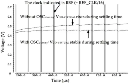
Secondly, OSCdiode includes both a primary oscillator (OSCmain) and a dummy oscillator
(OSCdummy), with the clock output derived from OSCmain. OSCdummy improves the load mismatch on
the VDD-VIRTUAL rail. When REF is high, OSCmain is enabled and consumes a specific amount of current.
During its low state, OSCmain does not oscillate, and its current consumption reduces, causing V DD-VIRTUAL to increase as shown in Figure 5. This causes OSCdiode to finally settle at the wrong frequency.
As a remedy, OSCdummy is enabled when OSCmain is disabled and vice-versa, which helps to maintain a
roughly constant current draw from VDD-VIRTUAL in both high and low states of REF. This enables
OSCmain to settle at the right frequency. A simulation of the above stabilization techniques is shown
in Figure 5.
New measurements were made for OSCucmp, the uncompensated DCO from [12], at a lower
supply voltage of 0.7 V, for comparison with OSCdiode. Firstly, the measured stability of OSCdiode is
2.51%/°C, which is better than OSCucmp, which has a stability of 3.42%/°C at 0.7 V. The previous
discussion on the TC explains the above results. The temperature stability of 1.67%/°C stated in [12] for OSCucmp was measured from the test chip implemented in [12] at 1.1 V supply voltage. In OSCucmp
[12], the most significant bit (MSB) for calibration (SAR bits) connects the oscillator delay element directly to VDD and only the remaining bits connect the oscillator to “off” leaking LVT transistors.
Furthermore, the finer delay elements in OSCucmp are powered directly by VDD that causes stability
degradation in OSCucmp at lower VDD. Secondly, our new OSCdiode has a power consumption of 20 nW Comparator SAR logic Locking circuit Digital storage REF_CLK DCO Divider REF REF REF_CLK DCO Comparator Out Time
Locking Locking Locking Done
Figure 4.(a) DCO architecture [12]: The locking circuit compares the frequencies of DCO and REF and then sets the digital storage bits of the DCO using Serial Approximation Register (SAR) logic. After all the bits are set, the DCO frequency is locked to REF_CLK frequency. (b) Frequency comparison [12]: A 5-bit counter counts the number of DCO cycles within a REF cycle. If DCO frequency is greater than REF, comparator output goes high and otherwise low.©(2012) IEEE. Adapted with permission from A. Shrivastava and B. H. Calhoun, A 150 nW, 5 ppm/˝C, 100 kHz On-Chip clock source for ultra low
power SoCs; published by Custom Integrated Circuits Conference (CICC), 2012 IEEE.
During locking, the instantaneous frequency of OSCdiodeis affected. Therefore, the re-locking can take place during the idle times of the sensor operation. The chip can also be designed to send an interrupt that halts its execution while calibrating the clock.
Two techniques are used to stabilize OSCdiode. First, OSCdioderequires sufficient time to stabilize after a change in the SAR bits. This is achieved by dividing REF_CLK by 16 (REF=REF_CLK/16) and allocating 1/16 of the REF period (1 REF_CLK cycle) for comparison and the other 15/16 of the REF period (15 REF_CLK cycles) to settle VDD-VIRTUAL. VDD-VIRTUAL takes more time to settle because of the diode charging it. Dividing REF_CLK by a number lower than 16 (such as dividing by 2 in OSCucmp[12], by 4 or by 8) results in insufficient time to stabilize it. This gives a longer time (15 REF_CLK cycles) for the VDD-VIRTUALrail to settle before the next comparison process sets the next SAR bit.
Secondly, OSCdiode includes both a primary oscillator (OSCmain) and a dummy oscillator
(OSCdummy), with the clock output derived from OSCmain. OSCdummyimproves the load mismatch
on the VDD-VIRTUALrail. When REF is high, OSCmainis enabled and consumes a specific amount of current. During its low state, OSCmaindoes not oscillate, and its current consumption reduces, causing
VDD-VIRTUAL to increase as shown in Figure5. This causes OSCdiodeto finally settle at the wrong
frequency. As a remedy, OSCdummyis enabled when OSCmainis disabled and vice-versa, which helps to maintain a roughly constant current draw from VDD-VIRTUALin both high and low states of REF. This enables OSCmainto settle at the right frequency. A simulation of the above stabilization techniques is shown in Figure5.
J. Low Power Electron. Appl. 2016, 6, 7 7 of 20
at 100 kHz frequency and 0.7 V supply voltage, which is lower than the power consumption of OSCucmp at 35 nW, measured at 0.7 V supply voltage, and 100 nW power consumption for OSCucmp at
1.1 V [12].
Figure 5. VDD-VIRTUAL rail stabilization for OSCdiode: REF_CLK is divided by 16 to give the VDD-VIRTUAL
rail sufficient time to settle before setting the next SAR bit. Without OSCdummy, VDD-VIRTUAL starts to
increase during the “low” time of REF_CLK/16 (settling time) causing the oscillator frequency to settle to a wrong value. With OSCdummy, the frequency settles to the right value as VDD-VIRTUAL is stabilized
by balancing the current draw.
Finally, OSCdiode also has an improved voltage stability of 0.1%/mV as compared to OSCucmp,
which has a voltage stability of 0.6%/mV. Supply sensitivity is discussed further in Section 3.6. Higher stabilities require lesser re-locking to the stable clock. The above factors make OSCdiode a better
candidate for the temperature-uncompensated oscillator in the clock system. The OSCdiode after
accurate configuration is used as the system clock meeting the power goals of an ULP system.
2.2. Temperature-Compensated Oscillator (OSCcmp)
OSCcmp is a current-controlled DCO implemented in [12] that is used as a
temperature-compensated oscillator in the system. In this paper, we discuss a summary of its key features. OSCcmp
frequency is determined by a constant current source Io and the capacitance CL as shown in Figure 6a
[12].
The constant current source Io is obtained by adding currents from a Proportional to Absolute
Temperature (PTAT) source and a Complementary to Absolute Temperature (CTAT) source [12]. In the PTAT source, the current increases with an increase in temperature. In the CTAT, the current decreases with an increase in temperature. The sum current Io of PTAT and CTAT stays constant and
it varies by only 1% over a 100 °C range across different process corners (SS, TT, FF, etc.), as shown in Figure 6b [12]. CL is a Metal-Insulator-Metal (MIM) cap and also has very small temperature
variation. Process variation in the current source may cause either the PTAT or the CTAT to dominate the other, making the total current Io temperature dependent. To balance these currents, the resistance
and subsequently the current of the PTAT circuit is configured using 5-bits of process control. To further compensate for the decrease in the period of oscillations at high temperature, a second-order compensation technique is employed. It consists of an off, low threshold MOS, as shown in Figure 6c, which forms a leakage pull-up path that adds charge to CL, thereby increasing the delay with
temperature. This leakage current is controlled by a 6-bit switch and inverter control, thereby regulating the variation in the off-transistors of the second-order compensation technique. The 5-bit process trimming bits and 6-bit second-order compensation bits are set externally during calibration. Together with the second-order compensation, high temperature stability was achieved for OSCcmp.
Figure 5. VDD-VIRTUAL rail stabilization for OSCdiode: REF_CLK is divided by 16 to give the
VDD-VIRTUAL rail sufficient time to settle before setting the next SAR bit. Without OSCdummy,
VDD-VIRTUAL starts to increase during the “low” time of REF_CLK/16 (settling time) causing the
oscillator frequency to settle to a wrong value. With OSCdummy, the frequency settles to the right value
as VDD-VIRTUALis stabilized by balancing the current draw.
New measurements were made for OSCucmp, the uncompensated DCO from [12], at a lower supply voltage of 0.7 V, for comparison with OSCdiode. Firstly, the measured stability of OSCdiodeis 2.51%/˝C, which is better than OSC
ucmp, which has a stability of 3.42%/˝C at 0.7 V. The previous discussion on the TC explains the above results. The temperature stability of 1.67%/˝C stated in [12] for OSCucmpwas measured from the test chip implemented in [12] at 1.1 V supply voltage. In OSCucmp[12], the most significant bit (MSB) for calibration (SAR bits) connects the oscillator delay element directly to VDDand only the remaining bits connect the oscillator to “off” leaking LVT transistors. Furthermore, the finer delay elements in OSCucmpare powered directly by VDDthat causes stability degradation in OSCucmpat lower VDD. Secondly, our new OSCdiodehas a power consumption of 20 nW at 100 kHz frequency and 0.7 V supply voltage, which is lower than the power consumption of OSCucmpat 35 nW, measured at 0.7 V supply voltage, and 100 nW power consumption for OSCucmpat 1.1 V [12].
Finally, OSCdiodealso has an improved voltage stability of 0.1%/mV as compared to OSCucmp, which has a voltage stability of 0.6%/mV. Supply sensitivity is discussed further in Section3.6. Higher stabilities require lesser re-locking to the stable clock. The above factors make OSCdiodea better candidate for the temperature-uncompensated oscillator in the clock system. The OSCdiodeafter accurate configuration is used as the system clock meeting the power goals of an ULP system. 2.2. Temperature-Compensated Oscillator (OSCcmp)
OSCcmp is a current-controlled DCO implemented in [12] that is used as a temperature-compensated oscillator in the system. In this paper, we discuss a summary of its key features. OSCcmpfrequency is determined by a constant current source Ioand the capacitance CLas shown in Figure6a [12].
The constant current source Iois obtained by adding currents from a Proportional to Absolute Temperature (PTAT) source and a Complementary to Absolute Temperature (CTAT) source [12]. In the PTAT source, the current increases with an increase in temperature. In the CTAT, the current decreases with an increase in temperature. The sum current Ioof PTAT and CTAT stays constant and it varies by only 1% over a 100˝C range across different process corners (SS, TT, FF, etc.), as shown in Figure6b [12]. CLis a Metal-Insulator-Metal (MIM) cap and also has very small temperature variation. Process variation in the current source may cause either the PTAT or the CTAT to dominate the other, making the total current Iotemperature dependent. To balance these currents, the resistance and subsequently
J. Low Power Electron. Appl. 2016, 6, 7 8 of 20
the current of the PTAT circuit is configured using 5-bits of process control. To further compensate for the decrease in the period of oscillations at high temperature, a second-order compensation technique is employed. It consists of an off, low threshold MOS, as shown in Figure6c, which forms a leakage pull-up path that adds charge to CL, thereby increasing the delay with temperature. This leakage current is controlled by a 6-bit switch and inverter control, thereby regulating the variation in the off-transistors of the second-order compensation technique. The 5-bit process trimming bits and 6-bit second-order compensation bits are set externally during calibration. Together with the second-order compensation, high temperature stability was achieved for OSCcmp.
J. Low Power Electron. Appl. 2016, 6, 7 8 of 19
Stability measurements were performed across 10 chips to be 5 ppm/°C from 20 °C to 40 °C (14 ppm/°C from 20 °C to 70 °C) at 1.1 V supply voltage [12] and 7 ppm/°C from 20 °C to 40 °C at 0.7 V. This DCO is well suited for the human body application temperature range for which it was designed. One such example of a device targeting body temperature range is an RFID batteryless sensor in a wireless human body temperature monitoring system in [15]. This DCO is operational from 0.7 V to 1.1 V, assuming that once the supply voltage is chosen it is maintained to be stable. This makes it readily usable in ULP nodes employing a wide range of voltages of operation such as [2].
(a) (b) (c)
Figure 6. Temperature-compensated OSCcmp [12]: (a) Frequency of the oscillations depends on the
current Io and the capacitance CL. The constant current Io is sum of PTAT and CTAT current sources
[12] MIM caps used for CL are also resistant to temperature variations. (b) Simulation result [12] shows
that I0 varies by only 1% for a 100 °C range. (c) Second-order Compensation [12]: A pull-up path for
adding charge to CL. © (2012) IEEE. Reproduced with permission from A. Shrivastava and B. H.
Calhoun, A 150 nW, 5 ppm/°C, 100 kHz On-Chip clock source for ultra low power SoCs; published by Custom Integrated Circuits Conference (CICC), 2012 IEEE.
2.3. Digital Control Block
In this work, a low-power digital control block was implemented to automate the locking of OSCdiode to OSCcmp. It controls the time interval between successive locks of OSCdiode to OSCcmp. The
digital block is designed using standard digital synthesis flow. We describe two locking modes: (a) a periodic (counter-based) locking scheme; and (b) a prediction (temperature-drift-based) locking scheme in which an algorithm is used to optimize the number of locks in the event of temperature drift. The periodic locking scheme was implemented on the prototype and the prediction locking scheme was verified off-chip. The two modes are described in the following subsections.
2.3.1. Counter-Based Locking Scheme
In the counter-based scheme, locking is achieved through a 32-bit programmable counter. After counting the number of cycles programmed in these registers, the digital block issues a signal to enable the locking of one DCO to another. This programmable counter controls the locking of OSCdiode
to OSCcmp in a periodic fashion. A 32-bit count register implies the capability to count 232 cycles. If the
digital block is run at the same frequency as that of the clock source (e.g., 100 kHz), the interval between the locking of OSCdiode to OSCcmp can be programmed to be any value between the minimum
locking time (3.68 ms), to the maximum time possible (11.93 h) in steps of the clock period (10 µs). After locking, a power-down signal is asserted to disable OSCcmp and save power. Its SAR bits are
retained to preserve calibration and frequency lock settings.
The start-up times of all the DCOs are in the range of a few microseconds, which has to be considered during powering up of OSCcmp for the next locking event. OSCcmp must be powered on for
a sufficient amount of time before the next round of locking starts to account for its settling time. The digital block takes this into account through a settle register in each counter. A power-up signal is issued at a programmable number of cycles prior to the commencement of the next lock. At a system clock frequency of 100 kHz, 1 settle bit is equivalent to 10 µs, which is sufficient time to start-up OSCcmp. The programmable nature of the count and settle registers in the digital block enables this
clock source system to be flexible for serving different application needs. This makes it possible for
Figure 6.Temperature-compensated OSCcmp[12]: (a) Frequency of the oscillations depends on the
current Ioand the capacitance CL. The constant current Iois sum of PTAT and CTAT current sources [12]
MIM caps used for CLare also resistant to temperature variations. (b) Simulation result [12] shows that
I0varies by only 1% for a 100˝C range. (c) Second-order Compensation [12]: A pull-up path for adding
charge to CL. ©(2012) IEEE. Reproduced with permission from A. Shrivastava and B. H. Calhoun,
A 150 nW, 5 ppm/˝C, 100 kHz On-Chip clock source for ultra low power SoCs; published by Custom
Integrated Circuits Conference (CICC), 2012 IEEE.
Stability measurements were performed across 10 chips to be 5 ppm/˝C from 20˝C to 40˝C (14 ppm/˝C from 20˝C to 70˝C) at 1.1 V supply voltage [12] and 7 ppm/˝C from 20˝C to 40˝C at 0.7 V. This DCO is well suited for the human body application temperature range for which it was designed. One such example of a device targeting body temperature range is an RFID batteryless sensor in a wireless human body temperature monitoring system in [15]. This DCO is operational from 0.7 V to 1.1 V, assuming that once the supply voltage is chosen it is maintained to be stable. This makes it readily usable in ULP nodes employing a wide range of voltages of operation such as [2]. 2.3. Digital Control Block
In this work, a low-power digital control block was implemented to automate the locking of
OSCdiodeto OSCcmp. It controls the time interval between successive locks of OSCdiodeto OSCcmp.
The digital block is designed using standard digital synthesis flow. We describe two locking modes: (a) a periodic (counter-based) locking scheme; and (b) a prediction (temperature-drift-based) locking scheme in which an algorithm is used to optimize the number of locks in the event of temperature drift. The periodic locking scheme was implemented on the prototype and the prediction locking scheme was verified off-chip. The two modes are described in the following subsections.
2.3.1. Counter-Based Locking Scheme
In the counter-based scheme, locking is achieved through a 32-bit programmable counter. After counting the number of cycles programmed in these registers, the digital block issues a signal to enable the locking of one DCO to another. This programmable counter controls the locking of
OSCdiodeto OSCcmpin a periodic fashion. A 32-bit count register implies the capability to count 232
cycles. If the digital block is run at the same frequency as that of the clock source (e.g., 100 kHz), the interval between the locking of OSCdiodeto OSCcmpcan be programmed to be any value between
the minimum locking time (3.68 ms), to the maximum time possible (11.93 h) in steps of the clock period (10 µs). After locking, a power-down signal is asserted to disable OSCcmpand save power. Its SAR bits are retained to preserve calibration and frequency lock settings.
The start-up times of all the DCOs are in the range of a few microseconds, which has to be considered during powering up of OSCcmpfor the next locking event. OSCcmpmust be powered on for a sufficient amount of time before the next round of locking starts to account for its settling time. The digital block takes this into account through a settle register in each counter. A power-up signal is issued at a programmable number of cycles prior to the commencement of the next lock. At a system clock frequency of 100 kHz, 1 settle bit is equivalent to 10 µs, which is sufficient time to start-up OSCcmp. The programmable nature of the count and settle registers in the digital block enables this clock source system to be flexible for serving different application needs. This makes it possible for the system to incorporate another oscillator with lower power or other better clock attributes, and following the above DCO architecture, to be able to easily replace the DCOs described in this paper. 2.3.2. Temperature-Drift-Based Locking Scheme
This locking scheme makes use of the temperature dependence of the SAR calibration bits. As temperature drifts, the frequency of the uncompensated oscillator drifts. When it is re-locked to the compensated clock, the difference in the current and previous value of SAR bits of the uncompensated oscillator indicates the amount of drift in clock frequency and thereby serves as a proxy for the change in the temperature since the last lock.
The SAR calibration bits are designed to be read and write enabled in this system. This makes it possible to read their values from successive locks. During successive locks, if the SAR bits are unchanged or if only the “fine” lower significant bits (LSBs) are changed, it implies that the temperature has not significantly changed since the previous lock. Hence, re-locking, which involves powering up the high-power OSCcmp, leads to unnecessary power consumption. In this prediction-locking scheme, we monitor the bits and perform locks based on the history of temperature change and a prediction algorithm. An algorithm implemented for a temperature drift-prediction based locking scheme is described below.
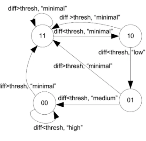
Figure7shows the state diagram of the implemented algorithm. The bubbles (11, 10, 01, and 00) represent the different locking states. Each state has a corresponding programmable counter threshold, which represents the time interval between successive locks. A minimal threshold (corresponding to 11) is the shortest interval between successive locks and a high threshold (corresponding to 00) is the longest locking interval. The low and medium thresholds are intermediate locking interval times and correspond to states 10 and 01, respectively. The SAR bits are monitored every time locking is performed. The initial locking state is “11” corresponding to the minimal locking interval, because there is no information on the temperature drift in the start. In all the successive locks, the difference between current SAR bits and previous SAR bits (diff ) determines the locking interval. If diff exceed a pre-programmed threshold value thresh, it means that a significant temperature drift has occurred.
If diff is greater than thresh, a lock is initiated and the locking state is reset to “11”, causing the next locking and monitoring to take place after a minimal interval. If diff is lesser than thresh, the locking state is decremented by 1, and the next locking happens after an increased time interval (low if the previous interval was minimal, medium if the previous interval was low, high if the previous interval was medium, and stays high if the previous interval was high). If at any point diff is greater than thresh, the locking state flips to “11”, thereby resetting the state machine. The circuit implementation of the algorithm was achieved using a digital synthesis flow. The functionality and power savings of the algorithm was verified using simulations, but was not implemented in the prototype. However, the reading out of SAR bits and variable locking intervals in this scheme was verified using chip measurements by implementing the algorithm in software.
J. Low Power Electron. Appl. 2016, 6, 7 10 of 20
J. Low Power Electron. Appl. 2016, 6, 7 9 of 19
the system to incorporate another oscillator with lower power or other better clock attributes, and following the above DCO architecture, to be able to easily replace the DCOs described in this paper.
2.3.2. Temperature-Drift-Based Locking Scheme
This locking scheme makes use of the temperature dependence of the SAR calibration bits. As temperature drifts, the frequency of the uncompensated oscillator drifts. When it is re-locked to the compensated clock, the difference in the current and previous value of SAR bits of the uncompensated oscillator indicates the amount of drift in clock frequency and thereby serves as a proxy for the change in the temperature since the last lock.
The SAR calibration bits are designed to be read and write enabled in this system. This makes it possible to read their values from successive locks. During successive locks, if the SAR bits are unchanged or if only the “fine” lower significant bits (LSBs) are changed, it implies that the temperature has not significantly changed since the previous lock. Hence, re-locking, which involves powering up the high-power OSCcmp, leads to unnecessary power consumption. In this
prediction-locking scheme, we monitor the bits and perform locks based on the history of temperature change and a prediction algorithm. An algorithm implemented for a temperature drift-prediction based locking scheme is described below.
Figure 7 shows the state diagram of the implemented algorithm. The bubbles (11, 10, 01, and 00) represent the different locking states. Each state has a corresponding programmable counter threshold, which represents the time interval between successive locks. A minimal threshold (corresponding to 11) is the shortest interval between successive locks and a high threshold (corresponding to 00) is the longest locking interval. The low and medium thresholds are intermediate locking interval times and correspond to states 10 and 01, respectively. The SAR bits are monitored every time locking is performed. The initial locking state is “11” corresponding to the minimal locking interval, because there is no information on the temperature drift in the start. In all the successive locks, the difference between current SAR bits and previous SAR bits (diff) determines the locking interval. If diff exceed a pre-programmed threshold value thresh, it means that a significant temperature drift has occurred.
Figure 7. A temperature-drift-based locking algorithm: The difference of the current and the previous SAR bits indicate the temperature drift. The locking interval is set according to the above state machine.
If diff is greater than thresh, a lock is initiated and the locking state is reset to “11”, causing the next locking and monitoring to take place after a minimal interval. If diff is lesser than thresh, the locking state is decremented by 1, and the next locking happens after an increased time interval (low if the previous interval was minimal, medium if the previous interval was low, high if the previous
Figure 7.A temperature-drift-based locking algorithm: The difference of the current and the previous SAR bits indicate the temperature drift. The locking interval is set according to the above state machine.
The digital block is operational at voltages ranging from 0.5 V to 1.1 V for a 100 kHz system frequency. For a count of 1 min, the measured power consumption of the digital block is 12 nW in the counter-based locking mode. The estimated power consumption of drift-based locking mode from simulations is 5.1 nW at 100 kHz with 0.7 V supply voltage. The power consumption for the temperature-drift-based locking mode is obtained from simulations because it was not implemented in the prototype. Operating the digital block at a lower frequency using a divided clock can further minimize this power consumption. To achieve the same locking interval time at a lower operating frequency, fewer count bits need to be set thereby lowering the switching activity. Further, if the digital block is run at a divided clock of 50 kHz, it can even be operational at 0.4 V supply voltage. At 50 kHz and 0.4 V, its power consumption goes down to 730 pW for the same locking interval and the power consumption of the overall clock source system in this case is 25 nW. Since there are only two signals (reset and power-down) interfacing the digital block to the oscillators and they toggle only once during each lock, they may be level-shifted to the oscillator domain without much loss of power. Hence, it is advantageous to operate the digital block in a sub-threshold voltage domain, which is usually available in ULP systems such as [2].
2.3.3. Power vs. Stability Analysis
The proposed programmable system allows us to analyze the power-stability trade-off, which we present in this subsection. We define the following parameters for our analysis:
1 Pdiode: OSCdiodestand-alone power.
2 Pcmp: OSCcmpstand-alone power.
3 Pdiode_lock: OSCdiodepower during locking (It is different from Pdiode).
4 Pcmp_leak: OSCcmpleakage power.
5 Pdig: Digital block power (includes both active and leakage power).
6 Tcmp_settle: OSCcmpsettling time after it is turned on (before the next locking commences).
7 Sdiode: OSCdiodestand-alone stability.
8 Scmp: OSCcmpstand-alone stability.
9 Tinterval: Time interval between consecutive locks.
10 Rtemp: Rate of temperature change. 11 Tlock: Total duration for all locks.
13 Ttotal: Sum of Tlockand Tnolock.
14 Tduration: Time duration of each lock.
OSCdiodeand digital block are “ON” for the whole duration, while OSCcmpis “ON” only for the
duration of the lock. The total system power consumption (Ptotal) can be estimated to be:
Ptotal “ ppPdiode`Pdig`Pcmp_leakq ˆTnolock` pPdiode_lock`Pdig`Pcmpq ˆTlock` pPcmpq ˆTcmp_settleq{Ttotal (7)
The digital block controls Tinterval, which relates to Tlockin Equation (1) as:
Tlock “ pTtotalˆTdurationq{Tinterval (8)
During no lock conditions, the oscillator frequency drift is given by Ddiode_nolockfor OSCdiodeand
Dcmp_nolockfor OSCcmp.
Ddiode_nolock “ SdiodeˆRtempˆTtotal (9)
Dcmp_nolock “ ScmpˆRtempˆTtotal (10)
In the duration of Ttotal, the total number of locks are n = Ttotal/Tinterval, where n is an integer. At the end of these locks (at time n ˆ Tinterval), OSCdiodewould have only drifted in the worst case as much as OSCcmp. During the remaining time (Ttotal– n ˆ Tinterval), the frequency drifts at the original rate for OSCdiode. The effective frequency drift during Ttotalcan be estimated as:
Dcmp_lock “ ScmpˆRtempˆn ˆ Tinterval `SdiodeˆRtempˆ pTtotal´n ˆ Tintervalq (11)
The maximum drift of frequencies between each lock (MaxDdiode_lock) is one approach to get the maximum frequency variation of the clock. This is equivalent to the net frequency drift during time interval between each lock (Tinterval):
MaxDdiode_lock “ SdiodeˆRtempˆTinterval (12)
From Equation (12), we observe that MaxDdiode_lockdecreases proportionally with Tinterval. Using the above equations, we are able to calculate the maximum frequency drift for any power budget, or the power consumption for any stability budget. If the rate of locking is greater than the rate of temperature change, the system power increases with no additional improvement in stability. This is because the stability of OSCdiodecannot exceed the stability of compensated oscillator OSCcmp. 3. Results
The system was fabricated in the 130 nm CMOS technology. The annotated die photo of the clock source is shown in Figure8a. The breakout dimensions are: 522 µm ˆ 215 µm for OSCcmp, 372 µm ˆ 238 µm for OSCdiode, and 179 µm ˆ 383 µm for the digital block. To implement the drift-based locking scheme, the estimated area is approximately 150 µm ˆ 150 µm. Uncompensated oscillator OSCucmpfrom [12] was also implemented for comparison to the proposed ULP oscillator
OSCdiode. The design layout showing the different components is shown in Figure8b. Results across
several chips for different aspects of the clock source system such as SAR calibration bits, frequency ranges, power, stability, jitter, and locking schemes are elaborated in the following sections.
J. Low Power Electron. Appl. 2016, 6, 7 12 of 20
J. Low Power Electron. Appl. 2016, 6, 7 11 of 19
Dcmp_nolock = Scmp × Rtemp × Ttotal (10)
In the duration of Ttotal, the total number of locks are n = Ttotal/Tinterval, where n is an integer. At the
end of these locks (at time n × Tinterval), OSCdiode would have only drifted in the worst case as much as
OSCcmp. During the remaining time (Ttotal – n × Tinterval), the frequency drifts at the original rate for
OSCdiode. The effective frequency drift during Ttotal can be estimated as:
Dcmp_lock = Scmp × Rtemp × n × Tinterval + Sdiode × Rtemp × (Ttotal − n × Tinterval) (11)
The maximum drift of frequencies between each lock (MaxDdiode_lock) is one approach to get the
maximum frequency variation of the clock. This is equivalent to the net frequency drift during time interval between each lock (Tinterval):
MaxDdiode_lock = Sdiode × Rtemp × Tinterval (12)
From Equation (12), we observe that MaxDdiode_lock decreases proportionally with Tinterval. Using
the above equations, we are able to calculate the maximum frequency drift for any power budget, or the power consumption for any stability budget. If the rate of locking is greater than the rate of temperature change, the system power increases with no additional improvement in stability. This is because the stability of OSCdiode cannot exceed the stability of compensated oscillator OSCcmp.
3. Results
The system was fabricated in the 130 nm CMOS technology. The annotated die photo of the clock source is shown in Figure 8a. The breakout dimensions are: 522 µm × 215 µm for OSCcmp, 372 µm ×
238 µm for OSCdiode, and 179 µm × 383 µm for the digital block. To implement the drift-based locking
scheme, the estimated area is approximately 150 µm × 150 µm. Uncompensated oscillator OSCucmp
from [12] was also implemented for comparison to the proposed ULP oscillator OSCdiode. The design
layout showing the different components is shown in Figure 8b. Results across several chips for different aspects of the clock source system such as SAR calibration bits, frequency ranges, power, stability, jitter, and locking schemes are elaborated in the following sections.
(a) (b)
Figure 8. (a) Annotated chip die photo. The design was implemented as a part of a larger test chip. The breakout dimensions are: 522 µm × 215 µm for OSCcmp, 372 µm × 238 µm for OSCdiode, and 179
µm × 383 µm for the digital block. The total system design area is 0.269 mm2. OSCucmp from [12] was
also implemented in this chip for evaluation and comparison with the proposed ULP OSCdiode. (b)
Design layout showing the breakdown components.
Figure 8.(a) Annotated chip die photo. The design was implemented as a part of a larger test chip. The breakout dimensions are: 522 µm ˆ 215 µm for OSCcmp, 372 µm ˆ 238 µm for OSCdiode, and
179 µm ˆ 383 µm for the digital block. The total system design area is 0.269 mm2. OSCucmpfrom [12]
was also implemented in this chip for evaluation and comparison with the proposed ULP OSCdiode.
(b) Design layout showing the breakdown components.
3.1. SAR Calibration Bits
To calibrate for a specific clock frequency during system start-up, the on-chip DCOs can be locked to an external stable clock source, such as an XTAL oscillator, that sets their SAR calibration registers. In this work, the calibration was performed at the supply voltage 0.7 V and room temperature (~27˝C). These SAR bits can also be manually set for achieving an initial system frequency. The SAR calibration bits are retained after every lock to preserve the locked frequency state. This means that every time the oscillator is powered down to save power and then powered-up for the next lock, it does not lose its calibrated frequency value. Hence, the external stable clock source is not required for the successive calibrations, making the system completely integrated. The DCO SAR registers are also read-enabled, which makes temperature drift-based locking possible. We are able to read, store, and compare successive SAR words to make a decision on the locking interval according to the temperature-drift algorithm. The write-enabled SAR registers make it possible to write in various values to switch between different frequencies. The system frequency is programmable which makes it suitable for dynamic frequency scaling (DFS) technique to save SoC processing power. In this test-chip, the bits to be written into the SAR registers are required to be scanned in serially through a scan chain. Therefore, the bits are scanned into the scan chain starting 23 cycles (corresponding to 23 SAR bits) earlier to the time at which the frequency switch is scheduled. There is a directly proportional relationship between the SAR bits and the oscillator frequency. To achieve higher frequencies for a particular supply voltage, more SAR bits are set. There is an inverse relationship between the SAR bits and the supply voltage. To achieve a particular frequency at a lower supply voltage, more SAR bits are set.
3.2. Frequency Range
The frequency ranges of both the uncompensated DCO (clock output) and the compensated DCO (clock that is locked to) limit the frequency range of the clock source system. The standalone frequency range of OSCcmpat 0.7 V supply voltage is 12 kHz to 150 kHz. Although the upper bound of OSCdiode goes up to 600 kHz, OSCcmp limits the system frequency range because of its lower upper-bound frequency. Thereby, the clock source system is capable of generating a clock in the range 12 kHz to 150 kHz at a supply voltage of 0.7 V. At 1.1 V, the frequency range is 30 kHz to 600 kHz. This programmable frequency range is useful in DFS for SoCs.
3.3. Power
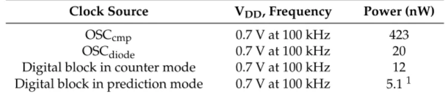
The average power consumption of the individual components of the proposed system at room temperature (~27˝C) is shown in Table1. OSC
cmp, OSCdiodeand the digital block have separate power supply pads, which make it possible to measure the current consumption of each individual block. A Keithley 2401 SourceMeter instrument DC power supply was used to precisely monitor power consumption over multiple locks and test chips. OSCcmposcillates only during locking during which we measure its total power and we measure only its leakage power when it is disabled during the interval between two locks. This total power consumption of the system is 36 nW at 0.7 V VDD, with the digital block operating in the counter-based locking scheme at 1 min locking interval. The system power consumption will be further lower for sub-threshold operation of the digital block at 0.4 V VDD. It can be generated from 0.7 V using low power switched capacitor converters, however, their design was not included in this test chip. To make such measurements at lower voltages possible separate VDDpads for different blocks were provided. In this case, for the same locking interval, the system power consumption is 25 nW, when OSCdiodewas locked to OSCcmp.
Table 1.Power consumption of components at room temperature (~27˝C).
Clock Source VDD, Frequency Power (nW)
OSCcmp 0.7 V at 100 kHz 423
OSCdiode 0.7 V at 100 kHz 20
Digital block in counter mode 0.7 V at 100 kHz 12 Digital block in prediction mode 0.7 V at 100 kHz 5.11
1The prediction mode was not realized in the prototype and the power is from simulations.
3.4. Jitter
We express RMS jitter in unit intervals (UI). The measured jitter is 0.0023 UIrmsfor OSCcmpand 0.0027 UIrms for OSCdiode, which is the clock output. It is better than [7] at 0.025 UIrms, and [16] at 0.024 UIrms, which were designed for sensor systems. The oscillator in [17] has lower jitter of 0.0014 UIrms, but it operates at sub-Hz frequency. It is important to understand the application space of the clock with jitter in the ns range. Digital blocks operating in the kHz frequency and in the sub-threshold or near-threshold voltage domain can be operational with the above clock when they are designed to meet the timing constraints. Jitter affects the clock path and can cause setup or hold violations in a digital system. Therefore, it is accounted for by specifying stringent constraints in the digital synthesis flow. Jitter is also highly crucial in data converter applications. For high-speed data converters operating at mega-samples per second speed (MSps), the clock jitter is required to be in the ps range. But in the ULP application space such as wearable technology, signals such as ECG (having bandwidth of up to 100 Hz) are sampled at the speed of few kilo samples per second (kSps). The data converters are able to operate at acceptable signal-to-noise ratios with RMS jitter numbers in the ns range (RMS jitter values in ns for OSCcmpis 23 ns and OSCdiodeis 27 ns). In the next section, we describe the effect of jitter on the stability of the clock source system.
3.5. Stability
The effective average stability of the clock source system equals the stability of OSCcmp, which is measured to be 7 ppm/˝C in the BSN compatible temperature range of 20˝C to 40˝C at 0.7 V. The demonstrated clock source system targets body sensor applications that experience only limited temperature variation as shown above. The proposed system is flexible to allow the DCOs to be replaced by improved versions of the DCO for high stability over a wider temperature range for other applications. In this section, we describe the dependence of the stability of the clock source system on the jitter of the temperature-compensated DCO. The jitter measurements are presented in the next subsection.


![Figure 4. (a) DCO architecture [12]: The locking circuit compares the frequencies of DCO and REF and then sets the digital storage bits of the DCO using Serial Approximation Register (SAR) logic](https://thumb-eu.123doks.com/thumbv2/123doknet/13800689.441083/7.892.121.767.128.535/figure-architecture-locking-circuit-compares-frequencies-approximation-register.webp)
![Figure 6. Temperature-compensated OSC cmp [12]: (a) Frequency of the oscillations depends on the current I o and the capacitance C L](https://thumb-eu.123doks.com/thumbv2/123doknet/13800689.441083/9.892.138.760.319.493/figure-temperature-compensated-frequency-oscillations-depends-current-capacitance.webp)