A 249-Mpixel/s HEVC Video-Decoder
Chip for 4K Ultra-HD Applications
The MIT Faculty has made this article openly available. Please share how this access benefits you. Your story matters.
Citation Tikekar, Mehul, Chao-Tsung Huang, Chiraag Juvekar, Vivienne Sze, and Anantha P. Chandrakasan. “A 249-Mpixel/s HEVC Video-Decoder Chip for 4K Ultra-HD Applications.” IEEE Journal of Solid-State Circuits 49, no. 1 (n.d.): 61–72.
As Published http://dx.doi.org/10.1109/jssc.2013.2284362
Publisher Institute of Electrical and Electronics Engineers (IEEE)
Version Author's final manuscript
Citable link http://hdl.handle.net/1721.1/93876
Terms of Use Creative Commons Attribution-Noncommercial-Share Alike
4K Ultra HD Applications
Mehul Tikekar, Student Member, IEEE, Chao-Tsung Huang, Member, IEEE,
Chiraag Juvekar, Student Member, IEEE, Vivienne Sze, Member, IEEE,
Anantha Chandrakasan, Fellow, IEEE
Abstract
High Efficiency Video Coding, the latest video standard, uses larger and variable-sized coding units and longer interpolation filters than H.264/AVC to better exploit redundancy in video signals. These algorithmic techniques enable a 50% decrease in bitrate at the cost of computational complexity, external memory bandwidth, and, for ASIC implementations, on-chip SRAM of the video codec. This paper describes architectural optimizations for an HEVC video decoder chip. The chip uses a two-stage sub-pipelining scheme to reduce on-chip SRAM by 56k bytes – a 32% reduction. A high-throughput read-only cache combined with DRAM-latency-aware memory mapping reduces DRAM bandwidth by 67%. The chip is built for HEVC Working Draft 4 Low Complexity configuration and occupies 1
.77 mm 2
in 40nm CMOS. It performs 4K Ultra HD 30 fps video decoding at 200 MHz while consuming 1.19 nJ/pixel of normalized system power.
Index Terms
High Efficiency Video Coding, ultra high definition, video-decoder chip, motion compensation cache, inverse discrete cosine transform, entropy decoder, DRAM bandwidth reduction
Author for Correspondence: Mehul Tikekar
50 Vassar Street, Room 38-107, Cambridge, MA 02139. Email: [email protected]
M. Tikekar, C. Juvekar, V. Sze and A. Chandrakasan are with Massachusetts Institute of Technology (MIT), Cambridge, MA 02139 USA
A 249 Mpixel/s HEVC Video-Decoder Chip for
4K Ultra HD Applications
I. INTRODUCTION
The decade since the introduction of H.264/AVC in 2003 has seen an explosion in the use of video for entertainment and work. Standard Definition (SD) and High Definition (720p HD) broadcasts are making way for Full HD (1080p), which in turn, are expected to be replaced by Ultra HD resolutions like 4K and 8K. Video traffic over the internet is growing rapidly and is expected to be about 86% of the global consumer internet traffic by 2016 [1]. These factors motivated the development of a new video standard that provides high coding efficiency while supporting large resolutions. High Efficiency Video Coding [2] (H.265/HEVC) is the successor video standard to the popular H.264/AVC. The first version of HEVC was ratified in January 2013 and it aims to provide a 50% reduction in bitrate at the same visual quality [3]. HEVC achieves this compression by improving upon existing coding tools and developing new tools.
While both standards use the basic scheme of inter-frame and intra-frame prediction, inverse transform, loop filter, and entropy coding, HEVC improves upon AVC in the following respects:
1) Hierarchical Coding Units: The picture is broken down into raster-scanned coding tree units (CTU) which are fixed to 64×64, 32×32 or 16×16 in each picture. The CTU may be split into four partitions in a recursive fashion down to coding units as small as 8×8. This recursive split into 4 partitions is called quad-tree. Within a CTU, the coding units may use a mix of intra and inter prediction which introduces new dependencies between intra and inter prediction processing. AVC, on the other hand, uses a fixed macroblock size of 16×16 which may use either all-inter or all-intra prediction.
2) Transform units (TU): Each coding unit is further recursively split into transform units. HEVC Main Profile uses square TUs from 32×32 down to 4×4 with discrete cosine transform for all sizes and discrete sine transform for 4×4. In addition, the pre-standard Working Draft 4 (WD4) [4] version implemented in this work also uses non-square TUs such as 32×8 and 16×4. This compares to the 8×8 and 4×4 transforms in AVC.
3) Prediction Units (PU): In HEVC, each CU may be partitioned into one, two or four prediction units. In all, up to 7 different types of partitions are possible. Compared to AVC, HEVC introduces 4 new asymmetric partitionings. Of these, only the square PUs may use intra-prediction, and all PUs can use inter-prediction. The diversity in CU sizes combines multiplicatively with the diversity in partitions thus giving 24 different PU sizes in HEVC Main Profile. On the other hand, the AVC macroblock can be partitioned into square blocks and symmetric blocks giving 7 types of macroblock partitions.
4) Intra Prediction: HEVC Main Profile uses 35 intra-prediction modes including planar, DC and 33 angular modes. HEVC WD4 uses one more mode called LMChroma where luma pixels are used to predict the chroma pixels. In comparison, AVC uses 10 intra-prediction modes.
5) Inter Prediction: PUs may be predicted from either one (uni-prediction) or two (bi-prediction) reference locations from up to 16 previously decoded frames. For luma prediction, HEVC uses an 8-tap interpolation filter compared to the 6-tap filter in AVC. The memory bandwidth overhead of longer interpolation filters is largest for the smallest PUs. The smallest PU in WD4 is 4×4, which would require up to two 11×11 reference pixel blocks. This is a 49% increase over the 9×9 reference block required for AVC. To alleviate this worst-case memory bandwidth increase, HEVC Main Profile does not use 4×4 PUs (i.e. partitioning an 8×8 CU into four 4×4 PUs is disallowed). Also, 8×4 and 4×8 PUs may only use uni-prediction.
6) Loop Filter: The deblocking filter in HEVC is significantly simpler than in AVC. The deblocking filter can use up to 4 input pixels on either side of the edge, and the edges lie on an 8×8 grid. As a result, adjacent edges can be filtered independently. In WD4, dependencies between computation of filter parameters of adjacent edges prevent parallel deblocking of 8×8 pixel blocks. This has been fixed in HEVC Main Profile. A new loop filter called “Sample Adaptive Offset” (SAO) is introduced by HEVC. This work does not implement the SAO filter.
7) Entropy Coding: AVC entropy coding uses either context-based adaptive binary arithmetic coding (CABAC) or context-adaptive variable length coding (CAVLC). In comparison, HEVC Main Profile uses only CABAC to simplify the design of compliant decoders.
HEVC’s decoding complexity is found to be between 1.4× – 2× of AVC [5] when measured in terms of cycle count for software. In hardware, however, the increased complexity of HEVC entails significant increase in hardware complexity over traditional H.264/AVC decoders, both at the top-level of the video decoder, and in the low-level processing blocks. For example, the
largest coding tree unit (CTU) is 16× larger than the AVC macroblock which increases on-chip SRAM required for pipelining. Similarly, the inverse transform block needs a 16× larger transpose memory and must be implemented in SRAM rather than registers to avoid a large area cost. The main contributions of this work, detailed in the following sections, can be summarised as follows:
1) A variable-size system pipeline is developed to reduce on-chip SRAM and handle different CTU sizes.
2) Unified processing engines for prediction and transform are designed to manage the large diversity of PU and TU sizes.
3) A four-parallel motion compensation (MC) cache is designed to address the increased DRAM requirements.
Results for an ASIC test chip with these ideas are presented. The chip supports HEVC Working Draft 4 Low Complexity mode without Sample Adaptive Offset. It has a throughput of 249 Mpixel/s when operating at 200 MHz, thus supporting 4K Ultra HD resolutions (3840×2160) at 30 fps.
II. VARIABLE-SIZESYSTEM PIPELINE
The main considerations for the system pipeline of the HEVC decoder are variable sizes of the coding tree units (CTU), large size of the largest CTU and variable latency of the DRAM. As mentioned before, HEVC can use CTUs of sizes 16×16, 32×32 and 64×64. The largest CTU needs 6KB to store its luma and chroma pixels with 8-bit precision. The transform coefficients and residue are computed with higher precision (16-bit and 9-bit, respectively) and require larger storage accordingly. Other information such as intra-prediction mode, inter-prediction motion vectors, etc. needs to be stored at a 4×4 granularity. Also, buffers are needed between processing blocks that talk to the DRAM in order to accommodate its variable latency. All of these require large pipeline buffers in SRAM and we implement several techniques to reduce their size as detailed below.
A. Variable-size Pipeline Blocks
We call the unit of pipelining between processing engines on the video decoder as variable-size pipeline block (VPB). VPB variable-size is 64×64 for 64×64 CTU, 64×32 for 32×32 CTU, and
64×16 for 16×16 CTU. Thus, the VPB is as tall as the CTU but its width is fixed to 64 for a unified control flow. In the case of a 16×16 CTU, the VPB stores four of them. The prediction engine can now predict the luma pixels of the entire VPB before predicting the chroma pixels. As compared to a CTU sized pipelining, this reduces the number of switches between luma and chroma processing. As luma and chroma pixels are stored in different DRAM rows, reducing the number of switches between them helps to reduce DRAM latency.
B. Split system pipeline
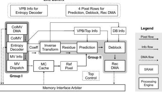
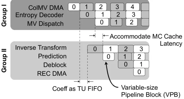
The issue of variable DRAM latency is especially problematic for motion compensation which makes the most number of accesses to the external DRAM. A motion compensation cache is used to reduce the bandwidth needed at the DRAM. This also improves the best-case latency to 3 cycles, which are needed for hit-miss resolution and cache read. However, the worse-case latency remains more or less unchanged thus increasing the overall variability seen by the prediction block. To deal with this, elastic pipelining must be used between the entropy decoder, which sends read requests to the cache, and prediction, which reads data from the cache. As a result, the system pipeline is broken into two groups. The first group contains the entropy decoder while the second contains inverse transform, prediction and the subsequent deblocking filter. This scheme is shown in Figure 1.
Entropy decoder uses collocated motion vectors from decoded pictures for motion vector prediction. A separate pipeline stage, ColMV DMA is added prior to entropy decoder to read collocated motion vectors from the DRAM. This isolates entropy decoder from the variable DRAM latency. Similarly, an extra stage, reconstruction DMA, is added after deblocking filter in the second pipeline group to write back fully reconstructed pixels to DRAM. Processing engines are pipelined with VPB granularity within each group as shown in Figure 2. Pipelining
across the groups is explained next.
1) Pipelining between entropy decoder and inverse transform: The entropy decoder must send residue coefficients and transform information such as quantization parameter and transform unit size to the inverse transform block. As residue coefficients use 16-bit precision, 12k bytes of SRAM is needed for luma and chroma coefficients of one VPB. For full pipelining, storage for two VPBs is needed so that entropy decoder can write coefficients and inverse transform can read coefficients of the previous VPB simultaneously. Thus, VPB pipelining would need 24k bytes
of SRAM. We avoid this by observing that the largest TU size is 32×32 (A 64×64 CU must split its transform quadtree at least once). Hence, it is possible to use a 2-TU buffer instead. In order to accommodate variable latency on the path between entropy decoder and prediction, this TU buffer is implemented as a FIFO. Further, it requires only 4k bytes, thus saving 20k bytes of SRAM.
2) Pipelining between entropy decoder and prediction: In HEVC, each CTU may contain a mix of inter and intra CUs. Intra-prediction of a CU needs CUs to its left and top to be partially reconstructed (i.e. predicted and residue-corrected but not in-loop filtered). To simplify the control flow for the various CU quad-trees and respect the previous dependency, we schedule prediction one VPB pipeline stage after inverse transform. As a side-effect, this increases the delay between entropy decoder and prediction. To account for this delay, an extra stage called MV dispatch is added to the first pipeline group after entropy decoder.
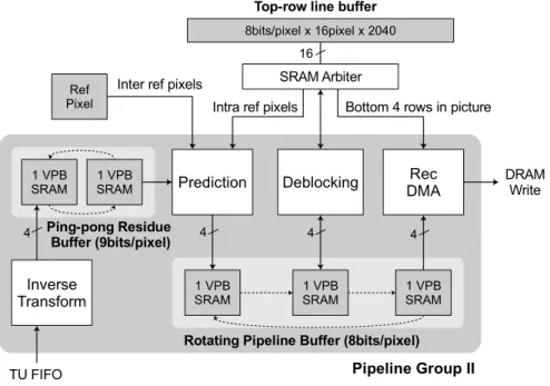
In the first pipeline group, a VPB-info line-buffer is used by entropy decoder for storing prediction information of upper row CTUs. In the second pipeline group, the 9-bit residues are passed from inverse transform to prediction using 2 VPB-sized SRAMs in ping-pong configura-tion. Prediction, deblocking and reconstruction DMA communicate using 3 VPB-sized SRAMs in a rotating buffer configuration as shown in Figure 3. A top-row line-buffer is used to store pre-deblocked pixels – 4 luma rows and 2 chroma rows from the CTUs above. One row is used as reference pixels for intra-prediction while all rows are used for deblocking. Deblocking filter also needs access to prediction and transform information such are prediction mode, motion vectors, reference picture indices, intra-prediction mode and quantization parameter to determine filter parameters. These are also stored in the same top-row line-buffer. As a special case, the last 4 rows in the picture are deblocked and stored in the same buffer without using any extra space. These are then accessed by the reconstruction DMA block and written out to the DRAM. DRAM writes are done in units of 8×4 pixels to improve MC cache efficiency, explained later in section IV. This requires two more rows of chroma to be stored in the line-buffer. The line-buffer is implemented as an SRAM 16-pixels wide and 2040 entries tall. Of these 2040 entries, four 3840 pixel-wide luma rows take 960 entries, eight 1920 pixel-wide chroma rows take 960 entries, and one row of prediction and transform information for deblocking takes 120 entries. To reduce area, a single-port SRAM is used and requests from prediction, deblocking and reconstruction DMA are arbitrated. The access patterns of the three blocks to the SRAM are
designed to minimize the amount of collisions and the arbitration scheme gives higher priority to the deblocking filter as it has a lower margin in the cycle budget. This minimizes the performance penalty of the SRAM sharing.
III. UNIFIEDPROCESSINGENGINES
A. Entropy Coding
This work implements HEVC WD4 Low Complexity entropy decoding using context-based adaptive variable length coding (CAVLC). The main challenge in HEVC entropy decoding is to meet the throughput requirement for all sizes of coding units (CU). Large coding units present a peculiar problem of being faster to decode, owing to better compression, but taking more time to write out the decoded information. To solve this problem, two methods are proposed.
1) SRAM redirect scheme: Mode information in transferred from entropy decoder to prediction at a fixed 4×4 pixel granularity, the size of the smallest PU. This simplifies control flow on the prediction side which can read mode information based only on the current position in the CTU irrespective of CU hierarchy and PU size. However, on the entropy decoder side, this is disadvantageous for large PUs as one needs to write multiple copies of the same mode information. To alleviate this problem, mode information is stored at a variable granularities of 4×4, 8×8, 4×16, 16×4 or 16×16. To keep reads simple, 6 bits per 16×16 block are used to encode the granularity. Then, based on the pixel location and granularity, the actual address in the SRAM is computed.
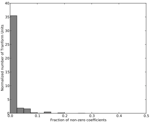
2) Zero flag for coefficients: Due to HEVC’s improved prediction, a large number of residue coefficients in a transform unit are found to be zero. As seen in the histogram in Figure 4, most transform units have less than 10% non-zero residue coefficients. The zero coefficients have a large decoding throughput than non-zero coefficients but take the same number of cycles to write out to the coeff SRAM. To match throughputs of decoding and writing out the non-zero coefficients, a separate register array is used to store zero flags. At the start of decoding a TU, all zero flags are set (all coefficients zero by default) and only non-zero coefficients are written to the coeff SRAM.
Although the final HEVC standard dropped CAVLC in favour of context-based adaptive binary arithmetic coding (CABAC), these proposed methods are useful for the CABAC coder as well.
B. Inverse Transform
The transform unit quad-tree starts from the coding unit and is recursively split into four partitions. In HEVC WD4, these partitions may be square or non-square. For example, a 2N ×2N quad-tree node may be split into four square N × N child nodes or four 2N × 0.5N nodes or four 0.5N × 2N nodes depending upon the prediction unit shape. The non-square nodes may also be split into square or non-square nodes. HEVC WD 4 uses eight transform unit (TU) sizes - T U32×32, T U16×16, T U8×8, T U4×4, T U32×8, T U8×32, T U16×4, and T U4×16. All these TUs use a fixed-point approximation of the type-2 Inverse discrete cosine transform (IDCT) with signed
8-bit coefficients. T U4×4 may also use a 4-point inverse discrete sine transform (IDST) if it
belongs to an intra-predicted CU. The main challenges in designing a HEVC inverse transform block as compared to AVC are explained next and our solutions are summarized.
1) 1-D Inverse Transform: HEVC IDCT and IDST matrices use 8-bit precision constants as compared to 5-bit constants for AVC. The constant multiplications can be implemented as shift-and-adds, where 8-bit constants would need at most 4 adds while the 5-bit constants need at most 2. Further, the largest 1-D transform in HEVC is the 32-point IDCT, compared to the 8-point IDCT in AVC. These two factors result in an 8×complexity increase in the transform logic. Some of this complexity increase is alleviated by the fact that the 32-point IDCT can be recursively decomposed into smaller IDCTs using a partial butterfly structure. However, even after this simplification, a single cycle 32-point IDCT was found to require 145k gates on synthesis in the target technology.
In this work, we perform partial matrix multiplication to compute a 1-D IDCT over multiple cycles. Normally, this would require replacing constant-multipliers by full-multipliers and con-stant look-up tables. For example, the 4×4 matrix-vector product that corresponds to the odd decomposition of the 8-pt IDCT can be computed over four cycles using four multipliers and four 4-entry look-up tables (4-LUTs) as shown in Figure 5. But we observe that the 16 constants contain only 4 unique numbers differing only in sign and order in each row. This enables us to use four constant multipliers. Further, these multipliers act on the same input coefficient, so they can be optimized using multiple constant multiplication [6]. Thus, four multipliers and four 4-LUTs are replaced by four adders. Similarly, the 8×8 and 16×16 matrix-vector products corresponding to odd decompositions of 16-pt and 32-pt IDCT can be implemented using 8 and
13 adders respectively. With this optimization, the total area of the IDCT is brought down by over 50% to 71k gates.
2) Transpose Memory using SRAM: In AVC decoders, transpose memory for inverse transform are usually implemented as a register array with multiplexers for column-write and row-read. In HEVC, however, a 32×32 transpose memory using a register array takes about 125k gates. To reduce area, the transpose memory is designed using four single-port SRAMs for a throughput of 4 pixel/cycle. When processing a new TU, the transpose memory is first written to by all the column transforms, and then, the row transform is performed by reading from the transpose memory. The transpose memory uses an interleaved memory mapping to write four pixels column-wise, but read them row-wise. This scheme suffers from a pipeline stall when switching from column to row transform due to the latency of writing the last column and the 1 cycle read latency of the SRAM. To avoid this, a small 36-pixel register store is used in parallel with the SRAMs.
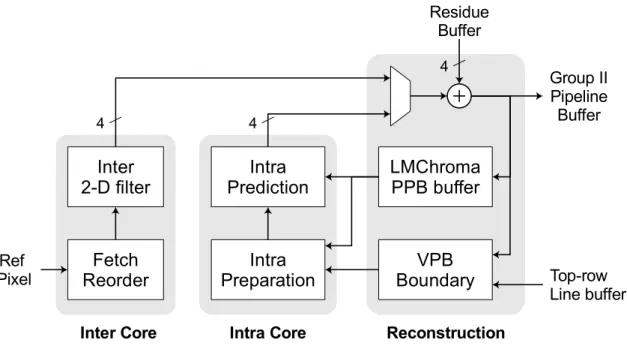
C. Prediction
As mentioned previously, a coding tree unit (CTU) may contain a mix of inter and intra-predicted coding units (CU). To support all intra/inter CU combinations in the same pipeline, we unify inter and intra-prediction blocks into a single prediction block. Their throughputs are aligned to 4 pixels/cycle allowing them to share the same reconstruction core as shown in Figure 6.
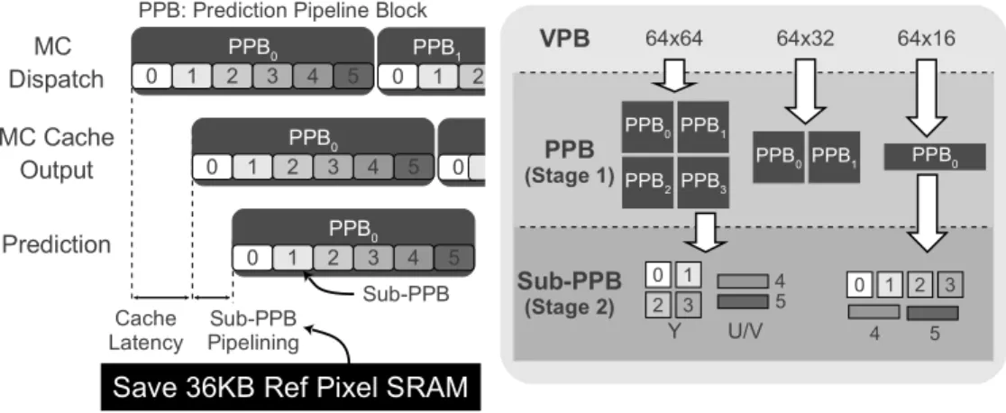
1) Intra Prediction: HEVC WD4 Intra-prediction uses 36 modes compared to 10 modes in AVC. Also, the largest PU is 64×64 which is 16 times larger than the AVC macroblock. To simplify decoding flow for all possible prediction unit (PU) sizes, the largest two VPBs are broken into 32×32 pipeline prediction blocks (PPB). Within each PPB, all luma pixels are predicted before chroma irrespective of PU sizes. HEVC WD4 can use luma pixels to predict chroma pixels in a mode called LMChroma. By breaking the VPB into four PPBs, the reconstructed luma reference buffer for LMChroma is reduced. A mode-adaptive scheduling scheme is developed to meet the required throughput of 2 pixels/cycle for all the intra modes.
2) Inter Prediction: Similar to intra-prediction, inter-prediction also splits the VPB into PPBs. However, fractional motion compensation requires many more reference pixels due to the longer interpolation filters in HEVC. To reduce SRAM for reference pixels, the PPBs are further broken
into sub-PPBs as shown in Figure 7. By avoiding PPB-level pipelining in inter-prediction, the size of the reference pixel buffer is brought down from 44k bytes to 8k bytes. Depending on pixel position and luma/chroma, one of 7 filters may be used by the interpolation filter. These filters are jointly optimized using time-multiplexed multiple constant multiplication for a 15% area reduction.
IV. MC CACHE WITH TWISTED 2D MAPPING
The 4K Ultra HD specification coupled with HEVC’s longer interpolation filters cause motion compensation to occupy a significant portion of the available DRAM bandwidth. To address this challenge we propose a MC cache which reuses reference pixel data shared amongst neighbouring inter PUs. In addition to reducing the bandwidth requirement of motion compensation, the cache also hides the variable latency of the DRAM. This provides a high throughput output to the prediction engine. Table I summarizes the main specifications of the proposed MC cache for our HEVC decoder.
A. Target DRAM System
Our target DRAM system is composed of two 64M×16-bit DDR3 DRAM modules with a 32 byte minimum access unit (MAU). We map a single MAU to a cache line. Consequently, our mapping can be reused with any DRAM system that uses 32-byte MAUs. The MAU addresses are 23-bits long and are split as: 13-bit row, 3-bit bank, 7-bit column. For simplicity, the DRAM controller and DDR3 interface are implemented on a Virtex-6 FPGA. We use the Xilinx MIG DRAM controller which supports a lazy precharge policy. Hence a row is only precharged when an access is made to a different row in the same bank.
B. DRAM Latency Aware Memory Map
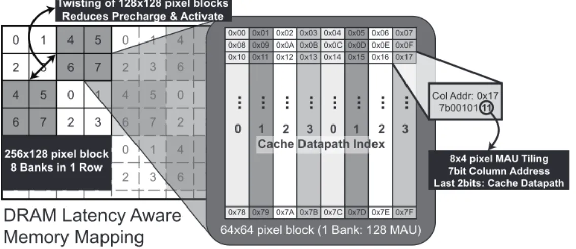
An ideal mapping of pixels to DRAM addresses should minimize the number of DRAM accesses and the latency experienced by each access. We accomplish these goals by minimizing the fetch of unused pixels and minimizing the number of row precharge/activate operations respectively. Additionally we map the DRAM addresses to cache lines such that the number of conflict misses is minimized.
Our latency aware memory mapping is shown in Figure 8. The luma color plane of a picture is tiled by 256×128 pixel blocks in raster scan order. Each block maps to an entire row across all eight banks. These blocks are then broken into eight 64×64 blocks which map to an individual bank in each row. Within each 64×64 block, 32-byte MAUs map to 8×4 pixel blocks that are tiled in a raster scan order. In Figure 8, the numbered square blocks correspond to 64×64 pixels and the numbers stand for the bank they belong to. Note how the mapping of 128×128 pixel blocks within each 256×128 regions alternates from left to right. Figure 8 shows this twisting behaviour for a 128×128 pixel region composed of four 64×64 blocks that map to banks 0, 1, 2 and 3.
The chroma color plane is stored in a similar manner in different rows. The only notable difference is that an 8×4 chroma MAU is composed of pixel-level interleaving of 4×4 Cr and Cb blocks. This is done to exploit the fact that Cb and Cr have the same reference region.
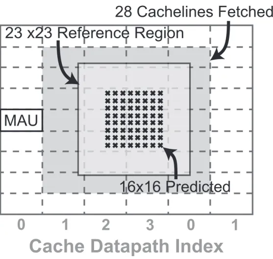
1) Minimizing fetch of unused pixels: Since the MAU size is 32 bytes each access fetches 32 pixels, some of which may not belong to the current reference region as seen in Figure 9. We minimize these by using an 8×4 MAU to exploit the rectangular geometry of the reference region. When compared with a 32×1 cache line this reduces the amount of unused pixels fetched for a given PU by 60% on average.
Since the fetched MAU are cached, unused pixels may be reused if they fall in the reference region of a neighbouring PU. Reference MAUs used for prediction at the right edge of a CTU can be reused when processing CTU to its right. However the lower CTU gets processed after an entire CTU row in the picture. Due to limited size of the cache, MAUs fetched at the bottom edge will be ejected and are not reused when predicting the lower CTU. When compared to 4×8 MAUs, 8×4 MAUs fetch more reusable pixels on the sides and less unused pixels on the bottom. As seen in Figure 10(a), this leads to a higher hit-rate. This effect is more pronounced for smaller CTU sizes where hit-rate may increase by up to 12%.
2) Minimizing row precharge and activation: Our proposed Twisted 2D mapping ensures that pixels in different DRAM rows in the same bank are at least 64 pixels away in both vertical and horizontal directions. It is unlikely that inter-prediction of two adjacent pixels will refer to two entries so far apart. Additionally a single dispatch request issued by the MC engine can at most cover 4 banks. It is possible to keep the corresponding rows in the four banks open and then fetch the required data. These two factors help us minimize the number of row changes.
Experiments show that twisting leads to a 20% saving in bandwidth over a direct mapping as seen in Table II
3) Minimizing conflict misses: We set the line index of a cache line to the 7 bit column address of the MAU. Thus there are no conflicts within a bank in a given row and closest conflicting addresses are 64 pixels apart. However there is a conflict between the same pixel location across different pictures. Similarly luma and chroma pixels may conflict if they are stored in the same column. Both these conflicts are tackled by ensuring sufficient associativity in the cache.
C. Four-Parallel Cache Architecture
This section describes the proposed micro-architecture of the four parallel MC cache. Our architecture achieves this high throughput through datapath parallelism and by hiding the variable DRAM latency. As seen in Figure 11, there are four parallel paths each outputting up to 32 pixels (1 MAU) per cycle. Queues on each path can store up to 32 outstanding requests.
1) Four-Parallel Data Flow: The parallelism in the cache datapath allows up to 4 MAUs in a row to be processed simultaneously. The MC cache must fetch at most 23×23 reference region corresponding to a 16×16 sub-PPB. This may require up to 7 cycles as shown in Figure 9. The address translation unit in Figure 11 reorders the MAUs based on the lowest 2 bits of the column address. This maps each request to a unique datapath and allows us to split the tag register file and cache SRAM into 4 smaller pieces. The cache tags for the missed cache lines are are immediately updated when the lines are requested from DRAM. This pre-emptive update ensures that future reads to the same cache line do not result in multiple requests to the DRAM.
2) Queue Management and Hazard Control: Each datapath has independent read and write queues which help absorb the variable DRAM latency. The 32 deep read queue stores pending requests to the SRAM. The 8 deep write queue stores pending cache misses which are yet to be resolved by the DRAM. The write queue is shorter because we expect fewer cache misses. Thus the cache allows for up to 32 pending requests to the DRAM. At the system level the latency of fetching the data from the DRAM is hidden by allowing for a seperate MV dispatch stage in the pipeline prior to the Prediction stage. Thus, while the reference data of a given block is being fetched, the previous block is undergoing prediction.
Since the cache system allows multiple pending reads, a read queue may have two reads for the same cache line resulting from two aliased MAUs. If the second read results in cache miss
a read-after-write hazard can occur when its data is written into the SRAM. The hazard control unit in Figure 11 avoids this by writing the data only after the first read is complete. This is accomplished by checking if the address of the first pending cache miss, matches any address stored in the read queue. Note, we only need to check the entries in the read queue that occur before the entry corresponding to this cache miss.
3) Cache Parameters: Figure 10(b) and Figure 10(c) shows the hit-rates observed as a function of the cache size and associativity respectively. A cache size of 16k bytes was chosen since it offered a good compromise between size and cache hit-rate. We selected a cache associativity of 4 because of the flexibility offered for Random Access frame structures. We observed that the performance of FIFO replacement is as good as Least Recently Used due to the relatively regular pattern of reference pixel data access. FIFO was chosen because of its simple implementation. We selected a unified luma and chroma cache because ensuring sufficient associativity allows us to accommodate both Random Access frame structures and different color planes.
D. Hit Rate Analysis, DRAM Bandwidth and Power
The rate at which data can be accessed from the DRAM depends on 2 factors: the number of bits that the DRAM interface can (theoretically) transfer per unit time and the pre-charge latency caused by the interaction between requests. We introduce the concepts of DATA BW and ACT BW to normalize the impact of these 2 factors. DATA BW refers to the amount of data that needs to be transferred from the DRAM to the decoder per unit time for real-time operation. Thus, a better hit-rate reduces the DATA BW. ACT BW is the amount of data that could have been transferred in the cycles that the DRAM was executing row change operation. Thus, a better memory map reduces the ACT BW. The advantage of defining DATA BW and ACT BW as mentioned above is that (DATA BW + ACT BW) is the minimum bandwidth required at the memory interface to support real-time operation. The performance of our cache is compared with two reference scenarios: a raster-scan address mapping and no cache and a 16KB cache with the same raster scan address mapping. As seen in Figure 12(a), using a 16KB cache reduces the Data BW by 55%. The Twisted 2D mapping reduces ACT BW by 71% of the ACT BW. Thus, our proposed cache results in a 67% reduction of the total DRAM bandwidth. Note that the theoretical maximum bandwidth of our DRAM system (two pieces of DDR3 operating at 400 MHz) is 3.2GB/s which cannot support a cacheless system. Using
a simplified power consumption model [7] based on the number of accesses, we find that the proposed cache saves up to 112mW. This is shown in Figure 12(b). The standby power is a significant fraction of the DRAM power consumption since the Xilinx DRAM controller does not implement a separate power-down mode.
Figure 12(c) compares the DRAM bandwidth across various encoder settings. We observe that smaller CTU sizes result in a larger bandwidth because of lower hit-rates. Thus larger CTU sizes such 64 can provide smaller external bandwidth at cost of higher on-chip complexity. We also note that the Random Access mode typically has lower hit rate when compared to the Low Delay mode. This behaviour is expected because the reference pictures are switched more frequently in the former.
V. IMPLEMENTATION AND TEST RESULTS
The core size is 1.77mm2 in 40nm CMOS, comprising 715K logic gates and 124KB of
on-chip SRAM. It is compliant to HEVC Test Model (HM) 4.0, and the supported decoding tools in HEVC Working Draft (WD) 4 are listed in Table III along with the main specs. This chip achieves 249Mpixels/s decoding throughput for 4K Ultra HD videos at 200MHz with the target DDR3 SDRAM operating at 400MHz. The core power is measured for six different configurations as shown in Figure 14. The average core power consumption for 4K Ultra HD decoding at 30fps is 76mW at 0.9V which corresponds to 0.31 nJ/pixel. The chip micrograph is shown in Figure 13 and the test system is shown in Figure 15. Logic and SRAM breakdown of the chip is shown in Figure 16. Similar to AVC decoders, we observe that prediction has the most significant resource utilization. However, we also observe that inverse transform is now significant due to the larger transform units while deblocking filter is relatively small due to simplifications in the standard. Power breakdown from post-layout power simulations with a bi-prediction bitstream is shown in Figure 17. We observe that the MC cache takes up a significant portion of the total power. However, the DRAM power saving due to the cache is about six times the cache’s own power consumption.
Table IV shows the comparison with state-of-the-art video decoders. We observe that the 2× compression efficiency of HEVC comes at a proportionate cost in logic area. The SRAM utilization is much higher due to larger coding units and use of on-chip line-buffers. Our cache and 2D twisted mapping help reduce normalized DRAM power in spite of increased memory
bandwidth. Despite the increased complexity, this work demonstrates the lowest normalized system power, which facilitates the use of HEVC on low-power portable devices for 4K Ultra HD applications.
VI. CONCLUSIONS
A video decoder for the latest High Efficiency Video Coding standard supporting Ultra HD resolution was presented. The main challenges of HEVC such as large coding tree units, hier-archical coding and transform units and increased memory bandwidth from longer interpolation filters were addressed in this work. In particular, a variable-sized split system pipeline was developed to process the wide range of coding tree unit sizes and account for variable DRAM latency. Unified processing engines for entropy decoding, inverse transform and prediction were designed to simplify the decoding flow for the entire range of coding, transform and prediction units. Mathematical features of the transform matrices were exploited to implement matrix-vector product with a 50% area reduction. Finally, a high-throughput motion compensation cache was designed in conjunction with a DRAM-aware memory map to provide 67% bandwidth savings. A summary of our contributions is given in Table V.
ACKNOWLEDGEMENTS
Funding was provided by Texas Instruments. The authors thank the TSMC University Shuttle Program for chip fabrication.
REFERENCES
[1] Cisco. (2012, May) Cisco visual networking index: Forecast and methodology, 2011 - 2016. [Online]. Available: http://www.cisco.com/en/US/solutions/collateral/ns341/ns525/ns537/ns705/ns827/white paper c11-481360.pdf
[2] G. Sullivan, J. Ohm, W.-J. Han, and T. Wiegand, “Overview of the high efficiency video coding (HEVC) standard,” IEEE Trans. Circuits Syst. Video Technol., vol. 22, no. 12, pp. 1649–1668, 2012.
[3] J. Ohm, G. Sullivan, H. Schwarz, T. K. Tan, and T. Wiegand, “Comparison of the coding efficiency of video coding standards - including high efficiency video coding (HEVC),” IEEE Trans. Circuits Syst. Video Technol., vol. 22, no. 12, pp. 1669–1684, 2012.
[4] B. Bross, W.-J. Han, J. Ohm, G. Sullivan, and T. Wiegand, “WD4: Working draft 4 of high-efficiency video coding,” Document JCTVC-F803, 2011.
[5] J. Vanne, M. Viitanen, T. Hamalainen, and A. Hallapuro, “Comparative rate-distortion-complexity analysis of HEVC and AVC video codecs,” IEEE Trans. Circuits Syst. Video Technol., vol. 22, no. 12, pp. 1885–1898, 2012.
[6] M. Puschel, J. M. F. Moura, J. Johnson, D. Padua, M. Veloso, B. Singer, J. Xiong, F. Franchetti, A. Gacic, Y. Voronenko, K. Chen, R. Johnson, and N. Rizzolo, “SPIRAL: code generation for DSP transforms,” Proc. IEEE, vol. 93, no. 2, pp. 232–275, 2005.
[7] Micron. DDR3 SDRAM system-power calculator. [Online]. Available: http://www.micron.com/products/support/power-calc [8] D. Zhou, J. Zhou, J. Zhu, P. Liu, and S. Goto, “A 2Gpixel/s H.264/AVC HP/MVC video decoder chip for super hi-vision
and 3DTV/FTV applications,” in IEEE Int. Solid-State Circuits Conf. (ISSCC) Dig. Tech. Papers, 2012, pp. 224–226. [9] D. Zhou, J. Zhou, X. He, J. Zhu, J. Kong, P. Liu, and S. Goto, “A 530 Mpixels/s 4096x2160@60fps H.264/AVC high
profile video decoder chip,” IEEE J. Solid-State Circuits, vol. 46, no. 4, pp. 777 –788, Apr. 2011.
[10] T.-D. Chuang, P.-K. Tsung, P.-C. Lin, L.-M. Chang, T.-C. Ma, Y.-H. Chen, and L.-G. Chen, “A 59.5mW scalable/multi-view video decoder chip for Quad/3D full HDTV and video streaming applications,” in IEEE Int. Solid-State Circuits Conf. (ISSCC) Dig. Tech. Papers, 2010, pp. 330–331.
[11] V. Sze, D. F. Finchelstein, M. E. Sinangil, and A. P. Chandrakasan, “A 0.7-v 1.8-mW H.264/AVC 720p video decoder,” IEEE J. Solid-State Circuits, vol. 44, no. 11, pp. 2943–2956, Nov. 2009.
[12] C. D. Chien, C. C. Lin, Y. H. Shih, H. C. Chen, C. J. Huang, C. Y. Yu, C. L. Chen, C. H. Cheng, and J. I. Guo, “A 252kgate/71mW multi-standard multi-channel video decoder for high definition video applications,” in IEEE Int. Solid-State Circuits Conf. (ISSCC) Dig. Tech. Papers, 2007, p. 282603.
[13] C. Lin, J. Guo, H. Chang, Y. Yang, J. Chen, M. Tsai, and J. Wang, “A 160kgate 4.5kB SRAM h.264 video decoder for HDTV applications,” in IEEE Int. Solid-State Circuits Conf. (ISSCC) Dig. Tech. Papers, 2006, pp. 1596–1605.
Mehul Tikekar (S’10) received the B.Tech degree in electrical engineering from the Indian institute of Technology Bombay, Mumbai, India, in 2010. He received the S.M. degree in electrical engineering and computer science at the Massachusetts Institute of Technology, Cambridge, in 2012 where he is currently pursuing the Ph.D. degree.
His research focuses on low power system design and hardware optimized video coding. Mr. Tikekar was a recipient of the MIT Presidential Fellowship in 2011.
Chao-Tsung Huang received the B.S. degree from Department of Electrical Engineering, National Taiwan University, in 2001, and the Ph.D. degree from Graduate Institute of Electronics Engineering, National Taiwan University, in 2005. He is now with National Tsing Hua University, Taiwan, as an assistant professor.
From 2005 to 2011, he worked for Novatek Microelectronics Corp., Taiwan, as a team leader responsible for developing multi-standard image and video codecs. He performed postdoctoral research on an HEVC decoder chip at Massachusetts Institute of Technology, Cambridge, from March 2011 to August 2012. He then worked on light-field camera design as his postdoctoral research at National Taiwan University, Taiwan, until July 2013.
His research interests include light-field signal processing and high performance video coding, especially from algorithm exploration to VLSI architecture design, chip implementation, and demo system. He received the MediaTek Fellowship from 2003 to 2005.
Chiraag Juvekar (S’12) received the B.Tech and M.Tech degrees in electrical engineering from the Indian institute of Technology Bombay, Mumbai, India, in 2012. He is currently pursuing the S.M. and Ph.D. degrees at Massachusetts Institute of Technology, Cambridge. His research focuses on low power system design, hardware optimized video coding and hardware security. Mr. Juvekar was a recipient of the MIT Presidential Fellowship in 2012.
Vivienne Sze (S’04-M’10) received the B.A.Sc. (Hons) degree in electrical engineering from the University of Toronto, Toronto, ON, Canada, in 2004, and the S.M. and Ph.D. degree in electrical engineering from the Massachusetts Institute of Technology (MIT), Cambridge, MA, in 2006 and 2010 respectively. She received the Jin-Au Kong Outstanding Doctoral Thesis Prize, awarded for the best Ph.D. thesis in electrical engineering at MIT in 2011.
Since August 2013, she has been with MIT as an Assistant Professor in the Electrical Engineering and Computer Science Department. Her research interests include energy efficient algorithms and architectures for portable multimedia applications. From September 2010 to July 2013, she was a Member of Technical Staff in the Systems and Applications R&D Center at Texas Instruments (TI), Dallas, TX, where she designed low-power algorithms and architectures for video coding. She also represented TI at the international JCT-VC standardization body developing HEVC, the next generation video coding standard. Within the committee, she was the primary coordinator of the core experiment on coefficient scanning and coding.
Dr. Sze was a recipient of the 2007 DAC/ISSCC Student Design Contest Award and a co-recipient of the 2008 A-SSCC Outstanding Design Award. She received the Natural Sciences and Engineering Research Council of Canada (NSERC) Julie Payette fellowship in 2004, the NSERC Postgraduate Scholarships in 2005 and 2007, and the Texas Instruments Graduate Woman’s Fellowship for Leadership in Microelectronics in 2008. In 2012, she was selected by IEEE-USA as one of the “New Faces of Engineering”.
Anantha P. Chandrakasan (M’95-SM’01-F’04) received the B.S, M.S. and Ph.D. degrees in Electrical Engineering and Computer Sciences from the University of California, Berkeley, in 1989, 1990, and 1994 respectively. Since September 1994, he has been with the Massachusetts Institute of Technology, Cambridge, where he is currently the Joseph F. and Nancy P. Keithley Professor of Electrical Engineering.
He was a co-recipient of several awards including the 1993 IEEE Communications Society’s Best Tutorial Paper Award, the IEEE Electron Devices Society’s 1997 Paul Rappaport Award for the Best Paper in an EDS publication during 1997, the 1999 DAC Design Contest Award, the 2004 DAC/ISSCC Student Design Contest Award, the 2007 ISSCC Beatrice Winner Award for Editorial Excellence and the ISSCC Jack Kilby Award for Outstanding Student Paper (2007, 2008, 2009). He received the 2009 Semiconductor Industry Association (SIA) University Researcher Award. He is the recipient of the 2013 IEEE Donald O. Pederson Award in Solid-State Circuits.
His research interests include micro-power digital and mixed-signal integrated circuit design, wireless microsensor system design, portable multimedia devices, energy efficient radios and emerging technologies. He is a co-author of Low Power Digital CMOS Design (Kluwer Academic Publishers, 1995), Digital Integrated Circuits (Pearson Prentice-Hall, 2003, 2nd edition), and Sub-threshold Design for Ultra-Low Power Systems (Springer 2006). He is also a co-editor of Low Power CMOS Design (IEEE Press, 1998), Design of High-Performance Microprocessor Circuits (IEEE Press, 2000), and Leakage in Nanometer CMOS Technologies (Springer, 2005).
He has served as a technical program co-chair for the 1997 International Symposium on Low Power Electronics and Design (ISLPED), VLSI Design ’98, and the 1998 IEEE Workshop on Signal Processing Systems. He was the Signal Processing Sub-committee Chair for ISSCC 1999-2001, the Program Vice-Chair for ISSCC 2002, the Program Chair for ISSCC 2003, the Technology Directions Sub-committee Chair for ISSCC 2004-2009, and the Conference Chair for ISSCC 2010-2012. He is the Conference Chair for ISSCC 2013. He was an Associate Editor for the IEEE Journal of Solid-State Circuits from 1998 to 2001. He served on SSCS AdCom from 2000 to 2007 and he was the meetings committee chair from 2004 to 2007. He was the Director of the MIT Microsystems Technology Laboratories from 2006 to 2011. Since July 2011, he is the Head of the MIT EECS Department.
LIST OFFIGURES
1 System pipelining for HEVC decoder . . . 22
2 Split system pipeline groups to address DRAM latency . . . 23
3 Memory management in second pipeline group . . . 24
4 Transform coefficient statistics . . . 25
5 4×4 matrix-vector product optimization . . . 26
6 Unified Prediction Engine Architecture . . . 27
7 Sub-PPB pipelining for inter-prediction . . . 28
8 Latency Aware DRAM mapping . . . 29
9 Example MC cache dispatch order . . . 30
10 Cache hit rate as a function of cache parameters . . . 31
11 Four-parallel cache architecture . . . 32
12 Comparison of DDR3 bandwidth and power consumption . . . 33
13 Chip Micrograph . . . 34
14 Core Power Measurements . . . 35
15 Test Setup for HEVC Video Decoder . . . 36
16 Logic and SRAM utilization . . . 37
LIST OFTABLES
I Overview of MC Cache Specifications . . . 39
II Comparison of Twisted 2D Mapping and Direct 2D Mapping . . . 40
III Chip Specifications . . . 41
IV Comparison with state-of-the-art video decoders . . . 42
VPB Info for Entropy Decoder Coeff Deblock MC Cache Rec DMA Ref Pixel
4 Pixel Rows for Prediction, Deblock, Rec DMA
Line Buffers
Residue Inverse
Transform Prediction
MV Info Group II
Memory Interface Arbiter Top Control ColMV ColMV DMA Group I Entropy Decoder MV Dispatch DB Info VPB/Top Info Pixel flow Info flow SRAM Processing Engine DMA flow Legend
Fig. 1. System pipelining for HEVC decoder. Coeff buffer saves 20k bytes of SRAM by TU pipelining. Connections to Line Buffers are omitted in the figure for clarity (see Figure 3 for details).
ColMV DMA
Entropy Decoder
MV Dispatch
0
1
2
3
0
1
2
0
1
2
3
0
1
2
0
1
0
Accommodate MC Cache
Latency
Inverse Transform
Prediction
Deblock
REC DMA
Variable-size
Pipeline Block (VPB)
Coeff as TU FIFO
0
1
2
3
4
G
ro
u
p
I
G
ro
u
p
I
I
Fig. 2. Split system pipeline to address variable DRAM latency. Within each group, variable-sized pipeline block-level pipelining is used.
1 VPB SRAM
Prediction Deblocking DMARec
SRAM Arbiter Inter ref pixels
DRAM Write Intra ref pixels Bottom 4 rows in picture
8bits/pixel x 16pixel x 2040
Rotating Pipeline Buffer (8bits/pixel)
4 4 4 16 1 VPB SRAM 1 VPB SRAM Inverse Transform Ref Pixel 1 VPB SRAM 1 VPB SRAM 4 Ping-pong Residue Buffer (9bits/pixel)
Top-row line buffer
TU FIFO Pipeline Group II
Fig. 3. Memory management in second pipeline group. A 2-VPB ping-pong and a 3-VPB rotating buffer are used as pipeline buffers. A single-port SRAM is used for top row buffer to save area and access to it is arbitrated. Marked bus widths denote SRAM data width in pixels (bytes).
0.0 0.1 0.2 0.3 0.4 0.5 Fraction of non-zero coefficients
0 5 10 15 20 25 30 35 40
Normalized number of Tranform Units
Fig. 4. Histogram of fraction of non-zero coefficients in transform units for Old Town Cross encoded in Random Access with 64×64 CTU and quantization parameter 35 ∼ 39. For this large quantization, most transform units have less than 10% non-zero coefficients.
i 18 75 50 89 Permute and Negate xi << 8 << 4 << 3 << 1 << 1 xi 18xi 75xi 50xi 89xi 9xi 25xi 64xi y0 y1 y2 y3 i = 0..3 18 50 75 89 -50 -89 -18 75 75 18 -89 50 -89 75 -50 18 xi Generic Implementation Exploiting features of HEVC matrix to use constant multipliers
Further optimization using MCM
Fig. 5. 4×4 matrix-vector product using multiple constant multiplication. The generic implementation uses four multipliers and 4-LUTs. HEVC-specific optimizations enable area-efficient implementation using 4 adders.
Inter 2-D filter Fetch Reorder Intra Prediction Intra Preparation LMChroma PPB buffer VPB Boundary Group II Pipeline Buffer Residue Buffer Ref Pixel Top-row Line buffer
Inter Core Intra Core Reconstruction
4 4
4
PPB0 0 1 2 3 4 5 MC Dispatch MC Cache Output Prediction Sub-PPB PPB: Prediction Pipeline Block
PPB1 0 1 2 PPB0 0 1 2 3 4 5 PPB0 0 1 2 3 4 5 0 Cache Latency Sub-PPB Pipelining
Save 36KB Ref Pixel SRAM
PPB0PPB1 PPB2PPB3 PPB0PPB1 PPB0 VPB 64x64 64x32 64x16 PPB (Stage 1) Sub-PPB (Stage 2) 0 1 2 3 4 5 Y U/V 0 1 2 3 4 5
Fig. 7. Variable-size pipeline blocks are broken down into sub-prediction pipeline blocks to save 36k bytes of SRAM in reference pixel storage
0 1 2 3 4 5 6 7 0 1 4 5 0 1 2 3 0 1 2 3 1 2 3 4 5 6 7 4 5 6 7 0 2 3 5 7 0 1 2 3 4 5 6 7 2 0 4 6 3 6 7 1 0x00 0x01 0x02 0x03 0x04 0x05 0x06 0x07 0x08 0x09 0x0A 0x0B 0x0C 0x0D 0x0E 0x0F 0x10 0x11 0x12 0x13 0x14 0x15 0x16 0x17 0x78 0x79 0x7A 0x7B 0x7C 0x7D 0x7E 0x7F .. . .. . .. . .. . .. . .. . .. . .. . Col Addr: 0x17 7b00101 11 Twisting of 128x128 pixel blocks
Reduces Precharge & Activate
256x128 pixel block 8 Banks in 1 Row
64x64 pixel block (1 Bank: 128 MAU)
DRAM Latency Aware Memory Mapping
8x4 pixel MAU Tiling 7bit Column Address Last 2bits: Cache Datapath
0 1 2 3 0 1
Cache Datapath Index
2 3
Fig. 8. Latency Aware DRAM mapping. 128 8×4 MAUs arranged in raster scan order make up one block. The twisted structure increases the horizontal distance between two rows in the same bank. Note how the MAU columns are partitioned into 4 datapaths (based on the last 2 bits of column address) of the four-parallel cache architecture.
MAU
16x16 Predicted
28 Cachelines Fetched
23 x23 Reference Region
0
1
2
3
0
1
Cache Datapath Index
Fig. 9. The example MC cache dispatch for a 23×23 reference region of a 16×16 sub-PPB. 7 cycles are required to fetch the 28 MAU at 4 MAU per cycle. Note that dispatch region need not be aligned with the four parallel cache datapaths, thus requiring a reordering. In this example, the region starts from datapath #1.
40% 50% 60% 70%
CTU-64 CTU-32 CTU-16
MAU 8x4 MAU 4x8
Hit Rate
(a) Cache line Geometry
40% 50% 60% 70% 4KB 8KB 16KB 32KB Hit Rate (b) Cache Size 40% 50% 60% 70%
1-way 2-way 4-way 8-way
Hit Rate
(c) Cache Associativity
Fig. 10. Cache hit rate as a function of CTU size, cache line geometry, cache-size and associativity. Experiments averaged over six sequences - Basketball Drive, Park Scene, Tennis, Crowd Run, Old Town Cross and Park Joy. The first are Full HD (240 pictures each) and the last three are 4K Ultra HD (120 pictures each). CTU size of 64 is used for the cache-size and associativity experiments.
Address
Translation ResolutionHit/Miss
Read & Write Queues Cache SRAM Banks DMA Control Tag Register File
Memory Interface Arbiter DMA Bus Four-Parallel MC Cache From Dispatch PredictionTo Hazard Detection Circuit WR Queue RD Queue ... Hn H1H0 To SRAM Hazard Detected RD index at WR queue head < i = RD Addr WR Addr Hit AND Hazard at ith RD: H i
Fig. 11. Proposed four-parallel MC cache architecture with 4 independent datapaths. The hazard detection circuit is shown in detail.
1627 738 738 1874 1475 428 0 1000 2000 3000 4000 RS Mapping + sPPB Sharing RS Mapping + 16KB Cache Proposed Cache ACT Data BW (Mbyte/s) 3501 2213 1166 -21% -55% -71%
(a) Bandwidth Comparison
90.4 90.4 90.4 123.5 56.0 56.0 57.0 44.9 0.0 100.0 200.0 300.0 RS Mapping + sPPB Sharing RS Mapping + 16KB Cache Proposed Cache ACT Data Standby Power (mW) 270.9 191.3 158.9 (b) Power Comparison 528 553 685 822 850 989 219 183 204 667 659 636 0 400 800 1200 1600 CTU-64 LD CTU-32 LD CTU-16 LD CTU-64 RA CTU-32 RA CTU-16 RA ACT Data BW (Mbyte/s) 747 889 1489 736 1509 1625 (c) BW across sequences
Fig. 12. Comparison of DDR3 bandwidth and power consumption across 3 scenarios. RS mapping maps all the MAUs in a raster scan order. ACT corresponds to the power and bandwidth induced by DRAM Precharge/Activate operations.
64x64/LD 32x32/LD 16x16/LD 64x64/RA 32x32/RA 16x16/RA 0 10 20 30 40 50 60 70 80 90 25 MHz (1280x720 30fps) 100 MHz (1920x1080 60fps) 200 MHz (3840x2160 30fps)
Encoding Configuration (CTU Size/Reference picture setting)
P o w e r (m W )
Fig. 14. Core power is measured for six different combinations - Random Access and Low Delay encoder configurations each with all three sizes of coding tree units. The core power is more or less constant due to our unified design.
Fig. 15. Test setup for HEVC video decoder. The chip is connected to Virtex-6 FPGA on Xilinx ML605 development board. The decoded 4K Ultra HD (3840×2160) output of the chip is displayed on four Full HD (1920×1080) monitors.
MC cache 126 Deblock 49.9 Entropy Decoder 94.5 Inverse Transform 121.1
Memory Interface Arbiter 13.7 Prediction 191.9 RegFiles 75.5 Others 42
(a) Logic utilization in kgates (total 715 kgates)
Pipeline Buffers 447.3 MC-related SRAM 200.4 Line Buffers 337 Others 32.8
(b) SRAM utilization in kbits (total 1018 kbits) Fig. 16. Logic and SRAM utilization for each processing engine.
Prediction 23% Deblocking 3% MC Cache 26% Inverse Transform 17%
Memory Interface Arbiter 2% Entropy Decoder 3% Line Buffers 2% Pipeline Buffers 10% Others 13%
TABLE I
OVERVIEW OFMC CACHESPECIFICATIONS
Cache line 32 Bytes (8×4 MAU) Cache SRAM 16KB (512 cache lines) Set-Associativity 4 Way
Tag Register File 128×70-bit Y/UV Scheme Unified cache Replacement Rule FIFO Policy DRAM Mapping Twisted 2D Mapping
TABLE II
COMPARISON OFTWISTED2D MAPPING ANDDIRECT2D MAPPING
Encoding Mode LD RA CTU Size 64 32 16 64 32 16 ACT BW Direct 2D 272 227 232 690 679 648 (MBytes/s) Twisted 2D 219 183 204 667 659 636 Gain 20% 20% 12% 3% 3% 2%
TABLE III
CHIPSPECIFICATIONS
Technology TSMC 40 nm CMOS Supply Voltage Core: 0.9 V, I/O: 2.5 V Chip Size 2.18mm×2.18mm Core Size 1.33mm×1.33mm Gate Count 715K (2-input NAND) On-Chip SRAM 124k bytes
Maximum Throughput 249 Mpixel/s @ 200 MHz
Decoding Tools
HEVC/H.265 WD4 (HM 4.0 low complexity w/o SAO) CTU size: 64×64, 32×32, 16×16
B-frame: Low Delay(LD)/Random Access(RA)
Symmetric and asymmetric motion partitions: 4×4 - 64×64 Square and non-square transform units: 4×4 - 32×32 All intra modes: DC, Planar, 33 Angular, LMChroma Measured Core Power
76 mW @ 0.9 V 200 MHz, 3840×2160 @ 30fps (average) 51 mW @ 0.9 V 100 MHz, 1920×1080 @ 60fps (average) 31 mW @ 0.9 V 25 MHz, 1280×720 @ 30fps (average)
TABLE IV
COMPARISON WITH STATE-OF-THE-ART VIDEO DECODERS
This Work ISSCC’12 [8] JSSC’11 [9] ISSCC’10 [10] JSSC’09 [11] ISSCC’07 [12] ISSCC’06 [13] Standard HEVC/H.265 WD4 H.264/AVC HP/MVC H.264 HP H.264/AVC HP SVC/MVC H.264/AVC BP JPEG, MPEG-1/2, MPEG-4, H.264 BP H.264/AVC MP Max Specification 3840×2160 @ 30fps 7860×4320 @ 60fps 4096x2160 @ 60fps 4096×2160 @ 24fps 1280×720 @ 30fps 1920×1088 @ 30fps 1920×1080 @ 30fps Gate count 715K 1338K 662K 414K 315K 252K 160K On-chip SRAM 124KB 80KB 60KB 9KB 17KB 5KB 5KB Technology 40nm/0.9V 65nm/1.2V 90nm/1.0V 90nm/1.0V 65nm/0.7V, 0.85V 130nm/1.2V 0.18µm/1.8V Core power 76mW 410mW 189mW 60mW 1.8mW 71mW 320mW Normalized core power
0.31nJ/pixel 0.21nJ/pixel 0.36nJ/pixel 0.28nJ/pixel 0.07nJ/pixel 1.13nJ/pixel 5.11nJ/pixel Normalized
DRAM power
0.88nJ/pixel 1.27nJ/pixel 1.11nJ/pixel N/A N/A N/A N/A Normalized
system power
1.19nJ/pixel 1.48nJ/pixel 1.47nJ/pixel N/A N/A N/A N/A DRAM
configuration
32b DDR3 64b DDR2 64b DDR N/A ZBT SRAM SDR 32b DDR + 32b SDR
TABLE V
SUMMARY OF CONTRIBUTIONS
HEVC/System feature Implementation challenge Proposed solution
Diverse CTU sizes Complicated control flow Variable-sized pipeline blocks
Large 64×64 CTU size Large pipeline buffers TU-pipelining between entropy and transform engines PPB-pipelining within prediction engine
Diverse PU, TU sizes Complicated control flow SRAM redirect scheme in entropy decoder Sub-PPB pipelining within prediction engine Unified transform processing engine
32×32 Largest TU size Large area of transform Multiple-constant multiplication for area reduction Longer interpolation filters High DRAM bandwidth High throughput MC cache design
Variable DRAM latency Pipeline stalls Split system pipeline