Accessible Broadband Network Analysis
by
Esa Han Hsien Masood
Submitted to the Department of Electrical Engineering and Computer Science
in Partial Fulfillment of the Requirements for the Degrees of
Bachelor of Science in Electrical Science and Engineering
and Master of Engineering in Electrical Engineering and Computer Science
at the Massachusetts Institute of Technology
May 10, 2002
Copyright 2002 Esa Han Hsien Masood. All rights reserved.
The author hereby grants to M.I.T. permission to reproduce and
distribute publicly paper and electronic copies of this thesis
and to grant others the right to do so. MASSACHUSETTS INSTUTE
BARKER
OFTECHNOLOGYJUL
3 12002
LIBRARIES
Author
Department of Electrical Engineering and Computer Science
May 10, 2002
Certified by
Neil Gershenfeld
Thesis Supervisor Accepted byArthur C. Smith
Chairman, Department Committee on Graduate Theses
Accessible Broadband Network Analysis
by
Esa Han Hsien Masood
Submitted to the
Department of Electrical Engineering and Computer Science
May 10, 2002
In Partial Fulfillment of the Requirements for the Degree of Bachelor of Science in Electrical Science and Engineering
and Master of Engineering in Electrical Engineering and Computer Science
Abstract
Radio frequency network analysis is a powerful and versatile analysis tool. Due to the extremely high cost of vector network analyzers and their lack of portability, their use has been limited exclusively to advanced engineering and laboratory applications. Deploying such forms of instrumentation on a large scale would require the cost of such instruments to be significantly reduced, while retaining a useful subset of their current functionality. We have developed an instrument that has a parts cost of $125, and is capable of carrying out basic reflection measurements across a large frequency range. In addition, we have applied this instrument to several test applications: Chipless RFID tag reading, milk quality analysis and postal mail content analysis, and have demonstrated the usefulness of this instrument for these applications. Aside from these applications, a portable and low-cost network analyzer provides an accessible platform for new and interesting applications of network analysis to be developed.
Thesis Supervisor: Neil Gershenfeld
Acknowledgements
In the name of God, most Compassionate, most Merciful.
I would like to express my sincere gratitude to the following people who have contributed tremendously to this thesis. My thesis advisor, Neil Gershenfeld for his direction and support for this project. Utmost thanks
as well to everyone in the Physics and Media Group as well as alumni, for all the ideas, assistance and company in lab: Ben, Ben, Dan, Matt, Yael, Jason, Rich, Rehmi, Caroline, Susan, John, Femi and Ravi. Special thanks to Rich Fletcher, who recruited me as a UROP and made me part of the Physics and Media
Group; Matt Reynolds for his ever willingness to help and his invaluable advice, especially when I first started off as a clueless UROP; and Yael Maguire for his brilliant Master's thesis which has served as a template for the writing up of this one.
In addition, I would like to thank my brothers, sisters as well as friends who have made the past few years of my education such a rewarding and memorable experience. I sincerely appreciate the moral and emotional support, especially in times when I'm faced with the seemingly impossible.
Finally, and most importantly, I would like to thank my parents for their years of untiring love, support and encouragement. They have given me so much, and to them I will always be indebted.
Table of Contents
1. INTR O DU CTIO N ... 6 2. D IELECTRIC CO NSTA NT TH EO RY ... 8 2.1 M ACROSCOPIC V IEW ... 8 2.2 M ICROSCOPIC V IEW ... 10 73 SU.MMARY 11 3. NETW O RK A NA LY ZER TH EO RY ... 133.1 CHARACTERIZING M AGNITUDE AND PHASE ... 13
3.2 TRANSM ISSION LINE BASICS... 14
M axim um Power transfer ... 15
Term inating Transm ission Lines ... 15
Reflection Param eters ... 16
The Sm ith Chart... 17
3.3 CHARACTERIZING UNKNOW N DEVICES... 18
3.4 GENERALIZED NETW ORK ANALYZER IMPLEMENTATION ... 20
Signal Source... 20
Signal Separation ... 21
Receiver ... 22
3.5 SUMMARY ... 22
4. SYSTEM DESIGN AND IMPLEMENTATION...23
4.1 DESIGN OBJECTIVES... 23
4.2 SYSTEM S LEVEL OVERVIEW ... 23
4.3 SIGNAL GENERATION ... 25
4.4 SIGNAL FILTERING ... 27
4.5 SIGNAL AMPLIFICATION ... 28
4.6 FRONT END DESIGN ... 29
4.7 PROBE COMPATIBILITY ... 32
4.8 SIGNAL D ETECTION... 33
4.9 SYSTEM CONTROL AND OPERATION... 35
4. 10 POW ER SUPPLY ... 36
4.11 INTERFACE AND D ATA D ISPLAY ... 37
4.12 PERFORMANCE AND SPECIFICATIONS ... 40
4.13 ANALYSIS OF DESIGN ... 41
5. TA G READ ER A PPLICA TIO N ... 43
5.1 BACKGROUND AND M OTIVATION... 43
5.2 SYSTEM D ESCRIPTION ... 46
5.3 EXPERIMENTAL SETUP ... 48
5.4 RESULTS... 49
5.5 ANALYSIS OF RESULTS... 53
5.6 SUMMARY ... 54
6. M A TERIA LS A NA LY SIS A PPLICA TION ... 56
6.1 BACKGROUND AND M OTIVATION... 56
6.2 SYSTEM D ESCRIPTION ... 61
6.3 EXPERIM ENTAL SETUP ... 64
6.4 RESULTS... 65
M ilk Quality Analysis Application... 65
Postal M ail Analysis Application ... 67
M ilk Quality Analysis Application ... 69
Postal M ail Analysis Application ... 70
6.6 SUMMARY ... 71 7. CONCLUSION ... 72 8. APPENDIX ... 73 8.1 BOARD SCHEMATICS ... 73 S h eet I ... 73 S h e et 2 ... 74
8.2 PRINTED CIRCUIT BOARD LAYOUT ... 75
Top Layer ... 75 Internal Plane I ... 76 Internal Plane 2 ... 77 Bottom Layer ... 78 8.3 M ICROCONTROLLER. CODE ... 79 8.4 M ICROCONTROLLER CONTROL ... 112 8.5 LABVIEW INTERFACE ... 119 User Panel ... 119 Diagram (Code) ... 120
8.6 LABVIEW INTERFACE FEATURES AND OPERATING INSTRUCTIONS ... 121
8.7 COST ANALYSIS OF BOARD ... 122
1. Introduction
Network analyzers are used extensively in laboratories to characterize both linear and non-linear behavior of electrical networks. As they provide both magnitude and phase measurements over a frequency range, they allow a complete characterization of the behavior of these networks. In addition to
characterizing electrical networks, the ability of network analyzers to provide complex impedance measurements allows the dielectric properties of materials to be inferred, and is increasingly becoming a useful instrument for materials characterization.
While the network analyzer is an extremely useful analysis tool, its use has been limited to the laboratory due to several factors. The most significant of these is the cost of such equipment: A network analyzer can cost within the range of $10,000 to $100,000, making it feasible only for industrial use or in research laboratories. In addition, network analyzers are bulky and are not suitable as portable analysis tools.
Furthermore, there is still much that is unknown about the full capabilities of network analysis. While other non-invasive probing techniques such as nuclear magnetic resonance (NMR), have been widely investigated and used in various medical imaging systems, frequency dependant complex
impedance analysis remains a largely untapped resource in terms of non-invasive analysis of materials. We believe that the reason for this is two fold: Firstly, there is a lack of knowledge of how network analyzers can be applied in the real world to solve common problems. Secondly, the lack of portable and
economically feasible network analyzers, that are able to perform dielectric analysis of materials, impedes efforts to find more widespread applications for network analyzers.
Thus, the aim of this thesis is to develop an instrument that possesses certain useful functions of network analyzers at a much lower cost than conventional models, and to demonstrate the usefulness of such a system on several applications. It is hoped that this investigation would illustrate new and useful
applications of network analysis, adding to the existing knowledgebase of known practical applications. In addition, we also hope to provide a feasible hardware platform, which would enable the further
investigation of new uses of broadband network analysis outside the laboratory.
There are currently several motivations for such an investigation. Firstly, considerable work has been done in our group in developing low-cost radio-frequency identification (RFID) tags as well as sensor tags, which are able to detect changes in the external environment. These tags essentially have resonant planar structures, and to date, network analyzers have been employed in reading these tags. Clearly, this is not a feasible method of tag reading, and thus more feasible broadband instrumentation is required in order for this RFID technology to be widely deployed.
A second motivation for this work would be the dielectric characterization of materials. In particular, through the collaboration of our group with Media Lab Asia (MLA), we have come to know that there is a demand for a feasible, non-invasive system that is able to provide a real-time analysis of milk quality. This is currently a problem in rural India, where farmers are paid based on the quality of their
yield. One approach to this problem would be to analyze the complex dielectric permittivity of the milk samples, and use that to determine useful physical properties of the milk being analyzed. Thus, we are interested in a system that can carry out frequency dependent complex analysis of materials, and distinguish between milk samples of varying grades. As a test case, we will use this system to analyze various milk samples to evaluate its effectiveness.
A second test case, in which we are currently interested, is related to providing security in postal mail. The United States Postal Service processes large amounts of mail each day, and there are security concerns regarding the content of the mail being processed. Currently, scanning of postal mail is being considered, in order to weed out any hazardous material that may be sent via the postal service. Present methods of scanning, such as metal detectors, can be used for such a large volume of mail. However, these methods do not provide sufficient information about mail content as a considerable amount of hazardous material are metallic in nature (e.g. plastic explosives). X-ray scanning and other forms of non-invasive imaging techniques, on the other hand are economically not feasible as they are labor intensive to operate and the cost of the requisite equipment is high. Thus, we propose employing frequency-dependent complex impedance analysis for this, and we will investigate the usefulness of the instrument on such an application.
This thesis will be structured as follows: Chapter 2 explains some of the physical mechanisms involved that determine the dielectric constant of a material, in order to provide some background with regard to materials. Chapter 3 introduces the concept of network analysis, and describes the basic concepts
involved as well as gives an overview of how commercial network analyzers are implemented. In Chapter 4, the design for the low-cost network analyzer board is presented. Also discussed are the way the different
subsystems within the design work, and the design choices that were made. Chapter 5 describes the tag reading application undertaken with this instrument, as well as provides results and analysis of these results. Chapter 6 provides a similar treatment for the materials analysis application. Chapter 7 then sums up this thesis.
2. Dielectric Constant Theory
Broadly speaking, materials can be grouped into several categories depending on their electrical properties. Materials in which the transport of electrons occur with ease, are termed conductors, while materials which allow the movement of electrons through their structures to a certain extent are termed semiconductors. Insulators (or dielectric materials) on the other hand do not permit the transport of electrons, and thus have low direct current (DC) conductivities.
2.1 Macroscopic View
Even though dielectrics do not have free electrons or mobile ions at the molecular level, interesting properties can nevertheless be observed in the presence of an electric field. The presence of large amounts of electric charge in a dielectric results in positive charge being pushed in one direction, and negative charge in the opposite direction, when an electric field is applied. The dielectric thus polarizes in the presence of an electric field, producing a net electric dipole moment per unit volume termed the polarization P. Polarization is a vector quantity, with units of Cm2 and is conventionally defined as
pointing from negative charge to positive charge.
+E
Figure 1. Polarization of a Dielectric in the Presence of an Electric Field
This transient charge motion when an electric field is applied, results in stored electrical energy within the dielectric material. The ability of dielectrics to store electrical energy is made use of in capacitors. Capacitors are used in numerous DC applications, such as in the flash unit of a camera, where charge storage and rapid release of the charge is necessary.
Figure 2. Parallel Plate Capacitor with Applied Voltage
1 While a brief treatment to this subject is given here, more comprehensive coverage can be found in most materials science textbooks on dielectric materials. The references used for this chapter can be found in the bibliography.
Consider the case of a capacitor with two parallel conducting plates of area A separated by a distance d. (Figure 2) Assume that nothing initially exists between the plates. Under these conditions, applying a voltage V across the capacitor will produce a charge Q on each plate given by CV, where C is the capacitance in farads, and C is given by:
C =-
EOA
d (2-1)
If a dielectric is now inserted between the plates, that completely fills the space, the electric field polarizes the dielectric and the resulting surface charge density P on the dielectric produces an internal electric field that opposes the applied field (Figure 2). This charge density also partially compensates the charge on the conducting plates. Maintaining a constant voltage across the plates results in more charge flowing onto the plates, and thus for the same voltage, there will be a greater charge Q' on each plate. Correspondingly, there will be an increase in capacitance and stored energy on the plates as well. The new capacitance, C' is given by:
,
Q'
LE,A EAV d d (2-2)
Where the increase in capacitance and charge is:
C' Q'-=-
= Er (2-3)
C
Q
which is the relative permittivity, or dielectric constant of the material. The dielectric constant of the material is unitless, whereas the permittivity of vacuum E, and the permittivity of the dielectric, E = Ej , are expressed in units of farads per meter. Dielectric constant can be related directly to the polarization P, since the surface charge on the dielectric equals the increase in charge on the plates:
(2-4)
PA =
Q'-Q
= C'V -CV = CV(E,. 1)Since C = 6 A /
d
andV
/d
is the electric field E between the plates of the capacitor,P = EOE(Er -1) and (2-5)
E, =1+ =I+ (2-6)
where
2
is the dielectric susceptibility.2.2 Microscopic View
The effect of an electric field on a dielectric can also be explained in terms of atomic behavior, by considering the microscopic effects of an applied electric field. In dielectrics, five major microscopic mechanisms operate when polarization occurs.
Electronic Polarization.
Atoms within the dielectric consist of positively charged nuclei surrounded by electron clouds. In the absence of an electric field, the statistical centers of positive and negative charge coincide. When an electric field is applied, there is a shift in the charge centers, particularly of the electrons. For a separation of J and a total charge of q , the atom has an induced dipole moment
p = qJ (2-7)
If there are N atoms per in3, the total electric dipole moment per unit volume of the material, its polarization, P, is given by:
P = Np = Nqd (2-8)
For moderate applied electric fields, the electric dipole moment of each atom is proportional to the field:
p =e ,E (2-9)
where the proportionality constant 0e is called the electronic polarizability (we assume here that the electric field felt by the atom is the same as the overall electric field applied to the dielectric). In purely covalent materials, such as diamond, this is usually the only source of polarization. From (2-6), ( 2-8 ) and (2-9 ), we get:
Na
Er =1+ Nae =1+(
'so ( 2-10 )
This equation relates a macroscopic material property, the dielectric constant, to a microscopic property, the electronic polarizability. In general, larger atoms are more polarizable, since they have a larger electron cloud around their nucleus, which gets more easily distorted by an electric field.
Ionic Polarization
In ionic materials such as Sodium Chloride (NaCI), in addition to the distortion of the electron clouds of each electron, an electric field pushes negatively charged chlorine ions in one direction, and positively charged sodium ions in the opposite direction. This results in some Na-Cl bonds being stretched, and others being compressed. As a consequence of this, there is another contribution to the polarizability of the dielectric,
aQ
, in equation ( 2-10 ). However, this contribution to polarization and dielectric constant cannot respond as quickly to rapidly changing fields as electronic polarization, since it involves the displacement of entire ions. This leads to a pronounced frequency dependence of the dielectric constant, aswill be discussed later.
Orientational (Dipolar) Polarization
Some molecules, like H20, have permanent dipole moments, and in the absence of a permanent electric field, they have no preferred direction of orientation. Applying an electric field causes these molecules to have a preferred orientation, and results in a further contribution to the polarization. In polar liquids such as water, this contribution is extremely significant at lower frequencies.
Interfacial (Space Charge) Polarization
In some dielectrics, electrons or ions can move more than interatomic distances, producing the build-up of layers of charge at internal interfaces such as grain boundaries or interphase boundaries. Such internal charge layers can make large contributions to the dielectric at low frequencies.
Ferroelectric Polarization
A few ionic crystals, called ferroelectrics, have symmetries that allow them to have a spontaneous ionic polarization in the absence of an electric field. In limited temperature ranges, some ferroelectrics, such as barium titanate and lead zirconium titanate (PZT), can have dielectric constants of several thousands.
2.3 Summary
The various microscopic mechanisms that have been described operate depending on the
frequency at which the material is probed. Furthermore, different materials have different mechanisms that predominate depending on the physical nature of the material. This property allows us to infer information about the physical characteristics of a material by probing them over a wide range of frequencies. We can make use of this principle to perform electromagnetic characterization of materials, allowing us to perform non-destructive analysis of materials and infer information about the physical nature of the material. The
topic of frequency dependence of the dielectric constant of materials will be elaborated on in chapter 6, where we discuss our investigation of the electromagnetic characterization of materials.
3. Network analyzer theory2
3.1 Characterizing Magnitude and Phase
Before approaching the subject of network analyzers, let us briefly address the more general topic of characterizing devices. That is, the kind of measurements we are interested in, the types of devices we can characterize and the instruments we can use for this.
Typically, characterizing a device involves measuring its linear and non-linear behavior. Since the number of devices is huge, and there are many attributes of each device that we might be interested in, a
large range of test equipment is required in order for all these attributes to be characterized. Figure 3 illustrates a model covering the wide range of measurements necessary for the complete linear and non-linear characterization of devices. Some instruments are optimized for only one test (e.g. Bit error rate), while others, such as network analyzers, are more general in nature. Network analyzers can measure both the linear and non-linear behavior of devices, although the measurement techniques are different.
Electrical devices that can be characterized using network analyzers include both passive and active devices. Examples of passive devices are resistors, capacitors and inductors, splitters, directional couplers and attenuators. Active devices would include transistors, oscillators, radio-frequency integrated circuits (RFICs) and modulators. Testing such devices is necessary, since they are often used as building blocks in larger systems, and we need to verify their specifications and performance before use.
In certain cases, magnitude-only measurements are sufficient. For example, the simple gain of an amplifier or stop-band rejection of a filter may be all the data we need. However, there are certainly other situations where phase information is critical. Thus, complete characterization of devices and networks involves measurement of phase as well as magnitude. Examples of this are: 1) The complex impedance of a device must be known for proper matching, 2) Models for circuit simulation require complex data, and 3) Time domain characterization requires magnitude and phase information to perform the inverse Fourier Transform.
Thus, we see that network analyzers are designed to be able to make complex impedance measurements of devices. Using appropriate probes, the complex impedance of materials can also be determined as will be elaborated on in Chapter 6.
2 This chapter presents a summary of the theory of network analyzers. More detailed coverage can be found in the references used for this chapter, as given in the bibliography.
Here is a key to many of the abbreviations used above:
Response
HP 84000 high-volume RFIC tester Dedicated (usually one-box) testers Vector signal analyzer
Spectrum analyzer Vector network analyzer
Tracldng generator/spectrun analyzer Scalar network analyzer
Noise-figure meter
Impedance analyzer (LCR meter) Power meter Diode detector/oscilloscope Measurement ACP AM-PM BER Compr'n Constell. EVM Eye GD Hann. Dist. NF Regrowth Rtn Ls VSWR
Adjacent channel power AM to PM conversion Bit-error rate Gain compression Constellation diagram Error-vector magnitude Eye diagram Group delay Harmonic distortion Noise figure Spectral regrowth Return loss
Voltage standing wave ratio
Figure 3. Model for Device Characterization3
3.2 Transmission Line Basics
The most fundamental concept of high-frequency networks analysis involves incident, reflected and transmitted waves traveling along transmission lines. At low frequencies, where the wavelengths of signals on the wire are much larger than the length of the conductor, a simple wire is very useful in carrying
3 Figure from "Network Analyzer Basics", by David Ballo, Hewlett-Packard Co, 1998.
Device Test Measurement Model
84000 ed. Testers E VNA TG/A SNA NF Mtr. Imped. An. Param. An. >owerMtr. E Det.scope r0
DC CW Swept Swept Noist 2-tone Multi- COMpIex Pulsed- Protocol
freg power tone mrnulation RF
Simple Stimulus type Complex
13
tLWLETV " 84000 Ded. Testers VSA SA VNA TG/SA SNA NF.Mtr. Imped. An. Power Mtr. Det/Scopepower. Current travels down the wire easily, and voltage and current are the same everywhere along the wire.
At high frequencies however, the wavelengths of signals are comparable to or much smaller than the length of the conductor, and the measured envelope voltage depends on the position on the line. Under these conditions, there is a need to use transmission lines in order to enable the efficient transfer of RF power. A transmission line takes on a certain characteristic (Z.), and this is determined by the geometry of the line. For example, in low power applications such as cable TV, coaxial transmission lines are designed to have a characteristic impedance of 75 ohms for low loss. For RF and microwave applications, where the high power might be encountered, coaxial transmission lines are designed to have a characteristic
impedance of 50 ohms, a compromise between maximum power handling (30 ohms) and low loss. In order to achieve maximum power transfer and low reflection, loads and sources have to be accurately matched to the characteristic impedance of the line.
Maximum Power transfer
Consider a source with a source impedence Rs, connected to a load, R1. We can show that, whether
the source is a DC voltage or a sinusoid, maximum power transfer into the load occurs when R, = R. Similarly for a transmission line, for the maximum transfer of energy into a transmission line from a source or from a transmission line to a load, the impedance of the source and load should match the characteristic impedance of the transmission line. Thus, in general, Z, is the target input and output impedances when designing devices and networks. When the source impedance is not purely resistive, maximum power transfer occurs when the load impedance is equal to the complex conjugate of the source impedance.
Terminating Transmission Lines
Depending on the impedance of the load terminating the transmission line, we observe various effects along the transmission line depending on the magnitude of the reflected wave. A transmission line terminated by an impedance equal to Z. results in maximum transfer of power to the load, and no reflected
signal occurs (i.e. magnitude of the reflected wave is zero). This is the same as if the transmission line were infinitely long. In this case, the envelope of the RF signal along the length of the line would be constant (no
standing wave pattern) since energy flow is in one direction only.
In the case where the transmission line is terminated by a short circuit, the absence of any resistive component in the load implies that no dissipation of power occurs. Since there is nowhere else for the
energy to go, a reflected wave is produced which travels back down the line towards the source (i.e. in a direction opposite to the incident wave). For a short circuit, the boundary condition at the end of the line requires the voltage there to be zero, and for this to occur, the reflected wave must be equal in magnitude to the incident wave and 1800 out of phase with it.
In the case where the termination is by an open circuit, Ohm's law implies that the open circuit can support no current. Therefore, the reflected current wave must be 180' out of phase with respect to the
incident wave (the reflected voltage wave will be in phase with the incident wave). This guarantees that the current at the open will be zero, and as in the previous case, the reflected voltage waves will be identical in magnitude but traveling in the opposite direction. For both these the short and open circuit cases, a
standing-wave pattern will be set up on the transmission line. The valleys of this standing-wave pattern will be zero and the peaks will be at twice the incident voltage level in both cases, with the positions of the peaks and valleys of the short and open being shifted along the line relative to each other.
In the case where the terminating impedance is a resistor that does not match the charactIisti impedance of the line, some of the incident energy will be absorbed on the load, while the rest will be reflected down the transmission line. We find that the reflected voltage wave will have an amplitude 1/3 of that of the incident wave, and the two waves will be 1800 out of phase with the load. The phase relationship between the incident and reflected wave will change as a function of distance along the transmission line
from the load, and the valleys of the standing wave pattern will no longer be zero and the peak will be less than that of the short/open case. The dependence of the standing wave pattern on the distance from the load, along the transmission line can be accounted for due to the variation of the effective impedance experienced by the traveling waves at different points on the transmission line. We can express the input impedance looking down the transmission line from the source as:
Z + jZ, tan
Zin
=Z2
(3-1)ZO +
jZ,
tan-where
A
is the wavelength of the traveling wave.Reflection Parameters
We can define several parameters for a particular transmission line and termination, based on the amplitudes of the incident and reflected waves. The reflection coefficient, ], is defined as:
V,_eete_ _ Zioad - Z
Vincident Zload +
Z-and is the ratio of the reflected signal voltage to the incident signal voltage. The magnitude portion of F is termed
p
, which has a range of values from 0 to 1. It is often convenient to show reflection on alogarithmic display, and this is often expressed as return loss:
Return loss is expressed in units of dB and is a scalar quantity. The definition of return loss includes a negative sign so that the return loss value is always a positive number. Return loss can be thought of as the number of dB that the reflected signal is below the incident signal, and this varies from infinity (for Z. impedance) to 0 (for open or short circuit).
As we have already seen, two waves traveling in opposite directions on the same media cause a "standing wave". This condition can be measured in terms of the voltage standing wave ratio (VSWR) and is defined as the maximum value of the RF envelope (peaks) over the minimum value of the envelope (valleys), and can also be expressed in terms of
p
:E
1+p
VSWR
= maxEnu 1-P (3-4)
VSWR can take on values between 1 and infinity.
The Smith Chart
By measuring the incident and reflected waves traveling down a transmission line, we see that a network analyzer can give us the complex reflection coefficient. However, we are typically interested in the impedance of the load terminating the transmission line (i.e. the device under test). It would be possible for us to calculate the complex impedance corresponding to each reflection coefficient value using ( 3-2 ), but this would give us a table of numbers which might be difficult to use. A simple graphical method to carry out this transformation was developed by Philip H. Smith in 1939. By mapping the impedance plane on to the polar plane, he devised the Smith Chart, which has become a ubiquitous in RF engineering design.
In this chart, the circles represent lines of constant resistance while arcs represent lines of constant reactance, with Z, corresponding to the center of the chart. To use the Smith chart, we use the value of
p
from the network analyzer to draw a circle on the chart, and the angle of I' to plot the appropriate radius onthe chart. The complex impedance of the load would then correspond to the point of intersection of the circle and radius. In general, Smith Charts are normalized to Z0, by dividing the impedance values by Z.
This allows the chart to be used independent of the characteristic impedance of the transmission line, if normalized values are used.
4 . 1* 11 . ... 4... . . .
V IY
to'o 80
RADIAL.Y SCALED PARAMETERS WAD TO 1s S 0 4 5 4 2 . 1 1 3 4 S.f 0? f ?. 10 12 14 29 30-. ..1.1 'Il0 A 01. . 2 3 4 10 100i6 .1 ,02 0.A 041 . A 1.5 3 454 1*0IS 10 . 2 . 0. 0.5 0 01 Ole . 09 1 1.1 12 A * , , ,;, , , 1.3 2
Figure 4. Smith Chart
3.3 Characterizing Unknown Devices
Network analysis is concerned with the accurate measurement of the ratio of the reflected signal to the incident signal and/or the transmitted signal to the incident signal for a particular signal transmitted into a system. More specifically, network analyzers characterize systems by measuring their scattering
parameters (S-parameters). S-parameters are widely used for characterizing high-frequency networks and can be related to familiar measurements such as gain, loss and reflection coefficient.
. 0.7 , 0 . . I. .0. , I . 0. 0 14 0.1 0.0 0 0 12 1.3 131. 1.6 1.7 IS 1.9 2 23 3 4 I 03 02 0. 0 1 0. 90.9 *0. 0.7 0.0.501 O5 00.0.1 S 4 3 23 2 I I yA 1 L .j_151 5 4 3 J -1900 op.0 ;0 31 2 I I . I I .
A particular two-port device or network has four S-parameters (in general, an N-port device or network has N2 parameters). These are determined by measuring the magnitude and phase of the transmitted and reflected signals for signals incident on each of the two ports, and calculating the appropriate ratios. For a particular device or network with ports
1
and 2, with incident signals a1 and a2respectively, two output signals can be obtained, which we term b, and b2. This is summarized in Figure 5.
Incident S2 1 Transmitted
a1 b2
S11 E Device Ref lected
Reflected Port 1 Port 2 S22
b1 a
2
Transmitted S12 Incident
Figure 5. Diagram summarizing inputs into a 2-port device and corresponding outputs. The relation of S-parameters to the various input and output signals are also illustrated.
SII and S2 1 can be determined by terminating port 2 with a matched load, and transmitting only signal a1.
Where we have: S11-Reflected b, (35) Incident a1 a2 = 0 and S Transmitted 2_ 2 Incident ala2 =0 (3-6)
S12 and S22 can be similarly determined. To summarize, the various S-parameters can be expressed as
follows (with common measurement terms in brackets):
SII = forward reflection coefficient (input match)
S22 = reverse reflection coefficient (output match)
S2 1 = forward transmission coefficient (gain or loss)
S12 = reverse transmission coefficient (isolation)
In terms of matrix notation, the S-parameters and the incident and reflected signals at the two ports can be expressed as:
b, _S1 S( a)
-I---, U ~ - - - --- ~-.--- - -~ - -~
-S-parameters have several advantages over other parameters used to characterize networks (such as H, Y or Z parameters, not covered here). Firstly, they do not require the connection of undesirable loads to the device under test. Secondly, the measured S-parameters of multiple devices can be cascaded to predict overall system performance. Thirdly, H, Y and Z parameters can be derived from S-parameters if desired. For RF design in particular, S-parameters are particularly important, as they can be easily imported and used with electronic simulation tools.
3.4
Generalized Network Analyzer Implementation
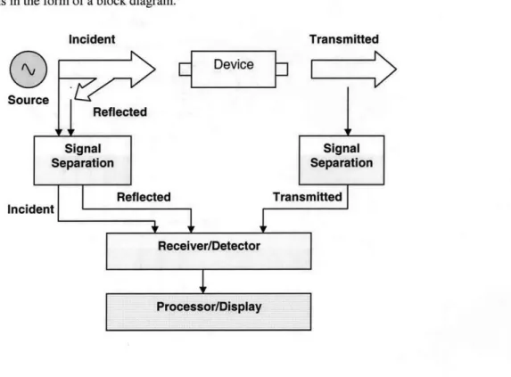
In general, network analyzers consist of: 1) a source for stimulus, 2) signal separation devices, 3) a receiver that provides detection and 4) a processor/display for calculating and reviewing the results. These four sections are required in order to measure the incident, reflected and transmitted signals. Figure 5
summarizes this in the form of a block diagram.
Incident Transmitted Device Source Reflected Signal Signal Separation Separation
I
Reflected Transmitted Incident I-Receiver/Detector Processor/DisplayFigure 6. Generalized Block Diagram of a Network Analyzer.
Signal Source
The source provides the stimulus signal for the purposes of testing, and by sweeping the source frequency the response of the device under test at various frequencies can be determined. Typically, these sources are based on open-loop voltage control oscillators (VCOs), which are cheaper, or more synthesized
sweepers, which provide higher performance especially for measuring narrowband components over small frequency spans.
Signal Separation
There are two functions of the signal separation devices. The first is to provide a reference signal that can be used to compare the measured signals. This can be done with splitters or directional couplers. Splitters are usually resistive, are non-directional devices and can be very broadband. The tradeoff is that they usually have 6 dB or more of loss in each arm. Directional couplers have low insertion loss and good isolation and directivity.
The second function of these devices is to, separate the incident (forward) and (reflected) reverse traveling waves at the input of the test device. This allows us to interpret the relevant parameters we wish to determine by comparing the incident and forward traveling waves. For this case, couplers are ideal as they are directional, have low loss and high reverse isolation. However, due to the difficulty of making broadband directional couplers, another method is often employed, which is to use a bridge.
Bridges are useful for measuring reflection as they can be made to operate over a broad range of frequencies. However, they are lossy and dissipate more of the transmitted signal compared to using directional couplers. Figure 7 shows a diagram of a resistive bridge.
I
Z
50 Vi + V.ut GND R R GNDFigure 7. Diagram of a Resistive Bridge
From the diagram, we can obtain the following expression for
V,,
V = V"Z VIn (3-8)
Z-+50 2
Solving for Vu, / Vin , we find that it is proportional to the reflection coefficient,
V Z - 50
Thus, if we can obtain both the phase difference between Kit and Vn as well as their amplitudes, the complex reflection coefficient can be determined. This in turn allows us to tell the complex impedance of the load using ( 3-2 ). However, the resistive bridge is often used as a scalar device to measure only the magnitude of the reflection coefficient. For this, diode detectors are used to obtain the amplitudes of V and Va4 .In network analyzers, the diode detector is built into the resistive network and the entire bridge
structure can be very small, so as to minimize the parasitic reactances. These parasitics serve to unbalance the bridge, and have to be reduced to ensure accuracy as well as a flat measurement baseline.
Receiver
Signal detection in network analyzers is carried out in one of two ways: The first of these is to use a diode detector, which converts an RF signal level to a proportional DC level. In the case that the signal is AC modulated, the diode strips the RF carrier from the modulation. Diode detection is inherently scalar, so only magnitude information is preserved and phase information is lost.
In order to preserve phase information, modern network analyzers uses a tuned receiver, where the RF signal is mixed down to a lower "intermediate" frequency (IF) signal using a local oscillator (LO). The IF signal is then converted to a digital signal using an analog-to-digital converter and processed using digital signal processing (DSP) techniques. This allows both phase and magnitude information to be extracted from the IF signal.
3.5 Summary
To summarize, a network analyzer is a useful tool for determining the S-parameters associated with a particular object under test. Determining this requires knowing how a transmitted signal is affected by the test object, in terms of phase and magnitude, and the various components of the network analyzer that was described, allow us to determine this. The next chapter presents a system that has been
implemented, which contains a useful portion of the functionality of commercial network analyzers. This instrument is capable of making reflection measurements, giving us some information about the SII parameter of a particular object under test. This in turn will allow us to infer other properties of the object, depending on the probe that is used and the application we are interested in, as will be explained in the subsequent chapters.
4. System Design and Implementation
This chapter describes the final design of the low-cost network analyzer that was implemented, as well as explains some of the design choices made. Where appropriate, less effective methods of prior designs that were attempted will be mentioned as well. We will first elaborate on the design objectives for our low-cost network analyzer, and then describe how the system works as a whole, before proceeding to explain each subsystem in detail. To conclude this chapter, the system that was implemented will be evaluated and the results from various tests will be presented.
4.1 Design Objectives
In terms of implementation, the aim of this work was to develop a low-cost RF network analyzer that can make simple
1-port
reflection measurements, providing spectral (phase and magnitude)information over a sufficiently broad range of frequencies. For this investigation, we are not concerned with precise reflection coefficient measurements or determining exact SI1 values. In designing the
instrument, several factors had to be considered. The first is the sweep range: this had to be sufficiently wide so that sufficient information could be gathered from the object under test. The second is sensitivity: The signal used to probe had to be of sufficient strength to allow small variations between different test objects to be detected. The third is cost: the parts cost had to be kept reasonably low (under $200 dollars). The fourth is related to the general ease of use of the system: The instrument had to be able to make quick measurements (i.e. be responsive to the user), output data in a usable form (such as to a PC where it could be displayed or stored) and have an appropriate software interface to support the hardware. In addition, having a user-friendly control interface would help make the instrument more accessible to a wider range of users who are unfamiliar with using laboratory measurement instruments.
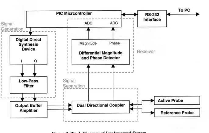
4.2 Systems Level Overview
Figure 8. shows the block diagram of the system, with the various stages involved. The operation of the entire instrument is controlled by a PIC microcontroller, which also allows the instrument to communicate with a PC via an RS-232 interface. The signal generation stage of the instrument was
implemented using a digital direct synthesis (DDS) chip, which is in turn controlled by the microcontroller. The DDS produces two signals: the in-phase signal (I) and a quadrature signal (Q) which is 900 out of phase with I. These two signals are then low-pass filtered, amplified and transmitted onto an appropriate probe. Of these two signals, one acts as the active signal and is transmitted to a probe that is exposed to the
tag or material being tested. The second signal, transmitted to a dummy probe, acts as a reference signal allowing us to detect changes in phase and magnitude of the active signal. A standing wave pattern is set up, on both the active and reference signal paths, with the amplitude and phase of the backward traveling wave dependant on the reflection coefficient of the load terminating that particular transmission line. Signal separation is achieved using a pair of directional-couplers to couple the backward traveling waves from the active and reference probes. These the two backward traveling waves are then compared by the receiver, which was implemented using a phase/magnitude detector chip. Comparing these two signals allows changes in the reflection coefficient to be detected, giving us information about changes in the physical environment at the probe. This chip converts differences in magnitude and phase of the two signals into a DC value, which is in turn read by the analog-to-digital converter (ADC) of the microcontroller, allowing the changes in phase and magnitude of the active signal at various points on the frequency spectrum to be converted into a digital value and read by the microcontroller. This in turn allows us to plot the phase and magnitude response spectra of a tag or object under test.
PIC Micrcontroller 4-* RS-232 ToPC 1
r- - - -- - - -- -- - -- - - - -- - Interface
Signal
ADC ADCGeneration_
Digital Direct
Synthesis Magnitude Phase
Device Rcie
Differential Magnitude Rec'iver
and Phase Detector SQ
Low-Pass Signal
Filter Separation
Active Probe Output Buffer Dual Directional Coupler
Amplifier Amplfid
Reference Probe
Figure 8. Block Diagram of Implemented System
The entire instrument was implemented on a single 4-layer, 0.062 inch printed circuit board, with the board size being 14.5 cm by 6.5 cm as shown in Figure 9.
Figure 9. Picture of Instrument Hardware.
4.3
Signal Generation
Two basic methods exist for signal generation. Traditionally, this has been done using the analog Phase-Locked-Loop (PLL), but recent advances in digital direct synthesis (DDS) technology has resulted in single-chip complete-DDS products being available at a low cost. Compared to the analog-PLL, the DDS method has many advantages, and has long been recognized as a superior technology in generating highly accurate, frequency-agile (rapidly changeable frequency over a wide range) low-distortion output waveforms. In addition, using a DDS allows the output frequency and phase to be precisely and rapidly manipulated under digital control. Aside from these two methods, a hybrid method is sometimes used as well, which employs a DDS to control an analog PLL. This method allows one to generate signals in the intermediate frequency (IF) range, since the upper limit of high-end DDS chips stop at the hundreds of megahertz to gigahertz range.
For the instrument, signal generation was carried out using a single chip DDS because of the need to generate a signal with a rapidly changing frequency. In addition, using a DDS offered a solution to having a signal generation stage that is able to operate at a wide frequency range. From experience, most analog-PLL implementations, which operate in the DC-200 megahertz range, are able to produce output signals with a bandwidth in the order of tens of megahertz (for example the MC145170 used in an earlier design operated in this frequency range and had a sweep span of 40MHz), and using a PLL to generate a wide enough frequency sweep would necessitate operating the PLL at a much higher frequency (in the gigahertz range), and mixing that frequency down to the desired range. Another issue that has to be addressed when using a PLL is that the frequency of the signal being generated is not known, and most counters (used to detect the frequency of the output signal) do not operate in the tens/hundreds of megahertz range. Thus, a divider/prescalar would have to be used to convert the sweep signal to a lower
frequency signal, before its frequency can be determined. All these factors would add more complexity to the design, and would have an impact on cost as well.
Of the DDS chips that are commercially available, the AD9854ASQ was finally selected. Previous versions were made using the AD985 1, which has a smaller frequency range than the AD9854, but worked well within its specified frequency range. The AD9852, which produces a single output frequency signal (i.e. instead of quadrature outputs) was also used in previous designs, and the reference and active signals were obtained by splitting the signal up into active and reference signals using a powIer s . There wcrc two disadvantages of this: Firstly, the splitter is lossy, thus attenuating of the output signal. Secondly, the reference and active signals were in phase, and this let to a clipping of the phase, due to the inability of the phase detector from distinguishing phase values of CD (this will be further explained in section 4.8 when the detector is described in more detail).
AD9854 digital-synthesizer operates at an internal clock rate up to 300 MHz, and contains two internal high-speed, high-performance quadrature 12-bit D/A converters, allowing the simultaneous generation of sine and cosine outputs. The AD9854's core provides 48-bit frequency resolution (1 microhertz tuning resolution with a 300 MHz system clock), and allows the generation of signals up to 150 MHz, which can be digitally tuned at the rate of 100 million new frequencies per second.
Other high-end DDS chips are also available, which provide a larger frequency sweep range than the AD9854, and were looked into. The top of the range DDS commercially available is the STEL-2375A, produced by ITT Industries. It operates at a clock frequency up to
1
GHz, and is capable of synthesizing waveforms between DC and 400 MHz, with a frequency resolution of 0.23 Hz. Another chip, the STEL-2373B operates at a clock frequency up to 800 MHz. It has 32-bit frequency resolution (0.186 Hz step size) and has a 0-320 MHz output frequency range. While it would have been desirable to have such a large swept frequency range, the cost of these chips greatly inhibited its use. The STEL-2373B for instance, costs $4,400 per chip (in quantities of 1-9) and thus would not be suitable for a low-cost design.With regards to implementation, the operation of the AD9854 was controlled by a microcontroller (PIC 16F876). The role of the microcontroller in controlling the DDS was firstly, to program several of the programming registers in the DDS chip. This set the clock frequency of operation, the internal clock multiplier of the DDS, output filter of the DDS, as well as powered down any unused stages in the DDS to reduce power consumption. This programming occurs when the system is powered up. The second function of the microcontroller is to control the frequency sweep of the DDS. The DDS was operated in the single-tone mode, and by specifying a particular frequency to the DDS the microcontroller causes the DDS to output a signal at that desired frequency. The frequency sweep was thus implemented by programming the PIC to specify a successively higher frequency to the DDS.
The AD9854 can be operated in either the serial or parallel programming mode. The parallel programming mode was opted for since it meant that that the DDS can be programmed at a much faster rate, allowing a faster frequency sweep. The trade-off for operating the DDS in the parallel programming mode was that it required more pins on the microcontroller, and hence a larger microcontroller. A total of
18 microcontroller pins were used to operate the DDS: 8 data input pins, 6 address input pins,
1
master reset pin, 1 serial/parallel mode select pin, 1 data write pin and 1 update clock pin.In order to conserve power, unused stages in the DDS can be powered down. For this application, the comparator stage of the DDS was powered down by setting the appropriate bit in the programming register of the DDS. The comparator is used to convert the output sinusoidal waveform into a square wave, and thus is not needed since this application requires as pure a sinusoidal output as possible.
Another issue that had to be observed when implementing the DDS was that of heat dissipation. Due to the operation of the DDS at such a high clock frequency, it had a power dissipation of over 3 Watts,
and precautions were taken in laying out the PCB and mounting the DDS chip. The 9854ASQ DDS chip is made with thermally enhanced packaging, with a heat sink at the bottom of the chip. Thus, the footprint of the chip had to have an exposed conducting surface, which was connected to the internal ground plane by
vias. When mounting the chip, solder paste was applied to the conducting surface first and the PCB was heated using a hotplate, and then cooled with the chip in place to establish a bond between the heat sink of the chip and the exposed conducting surface of the PCB. This allowed for heat to be conducted away from the chip to the board, and through the ground and power planes in the board, preventing the chip from overheating during continuous operation.
The actual implementation of the DDS chip required several other external passive components. Majority of these were bypass capacitors (0.1 uF chip capacitors). In addition to these, an RC filter was also used to filter the signal of the internal PLL of the DDS. A 2 kQ resistor was also used to specify the output current of the DDS: The DDS was operated slightly under the maximum output current rating in order to achieve maximum output signal strength without overloading the DDS. A 50 MHz crystal oscillator was also used as a reference clock for the internal clock. Together with an internal clock multiplier set at a factor of 6, the DDS was operated at an internal clock frequency of 300 MHz.
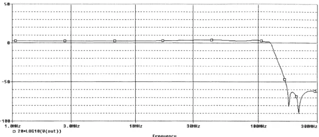
4.4 Signal Filtering
Low-pass filtering of both the output signals of the DDS is essential since several higher
frequency components are produced along with the fundamental signal being generated. In addition to the desired signal of frequency f., being generated, the output signal of the DDS contains frequency
components at fc, the internal clock frequency of the DDS, as well as frequency components at fc-f. and fc+f0. At a clock frequency of 300 MHz, and producing an output of 125 MHz, unwanted frequency
components occur at 175 MHz, 300 MHz and 425 MHz. Thus a low-pass filter with a sharp enough cut-off is necessary so as to ensure that the signal of interest is preserved, while sufficiently attenuating the higher frequency signals.
A three-stage L-C filter was used, as recommended by the datasheet for the AD9854, and this was found to sufficiently remove the higher frequency components of the DDS output signal. The magnitude
Bode plot of the filter used is shown in Figure 7, while the schematic for the output filter, along with component values, can be found in the Appendix.
-100
1..HHz 3.014Hz 1131Hz 3014Hz 1001MHz 30014Hz
El 20*LUC1O(U(out))
Frequency
Figure 10. Bode Plot (Magnitude) for Low Pass Filter
4.5 Signal Amplification
The signal produced by the DDS
varies
depending on frequency, with the amplitude of the signal being in the range of 440 to 640 mV peak-to-peak. This signal is further attenuated by thelow-pass
filter stage, and thus has insufficient power to be used directly. In order to allow the instrument to have sufficient sensitivity, the signals in the two signal paths were amplified before being channeled into the antenna. While a larger signal would allow the instrument to have greater sensitivity, this comes at an expenseof
higher power consumption. In addition, for the method of amplification used, there exists a trade-off between the amount of gain possible and the
operating
bandwidth of the amplifier. This places alimit
on theoptimal
amount of gain of the amplifier stage.The biggest design challenge for
our
application is the need for the amplifier to be able to amplify input signals from DCup
to about 150 megahertz, with relatively constant gain throughout the spectrum of frequencies. In addition, theoutput
had to have a sufficientlylarge
amplitude to be useful for the testapplications.
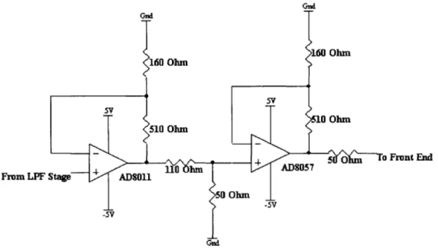
Several amplifier designs were experimented with, and the final design employed a two-stage, positive-feedback
operational
amplifier configuration. The op-amps used were the AD8O1 1 for the firstamplification stage, and the AD8057 for the second amplification stage. Both amplifiers are high speed, wide bandwidth
op-amps,
and operate off a ±5 V supply voltage. A two-stage configuration was adopted, insteadof
a single-stage configuration, so that the gain on each individual amplification stage could be reduced to achieve the same total output gain. This allowed the amplifier stage would have a betterfrequency response. The AD8057 was cascaded after the AD801 1, as it is a higher power amplifier compared to the AD801 1. Other factors that help improve the frequency response characteristics of the amplifier stage include using a positive feedback configuration instead of a negative feedback
configuration, minimizing the resistance of the feedback resistor, and using higher supply voltages for the op-amps.
Figure 11 shows the implementation of the two-stage design for a single signal path.
GMm 160 Ohm 160 Ohm 5V 5V 10 Ohm 510 OhmOhm 1 A 5 o Font End Fmm LPF Stage / ADS011 0 Ohm .sV -5v GMd
Figure 11. Schematic of Output Amplifier Stage
A previous design was attempted using a single output amplification stage using the AD801 1. But this required the gain of the single stage to be very high, causing the gain of the amplification stage to fall off significantly at higher frequencies. This was thus abandoned for a two-stage output amplifier.
4.6 Front End Design
The role of the front end is to achieve signal separation between the forward and backward traveling waves on the transmission line. This would in turn allow us to determine the reflection
coefficient, and from that, various properties of the load terminating the transmission line. Two methods are commonly used for signal separation, as mentioned in the previous chapter, namely using directional couplers and using a bridge. The advantage of directional couplers is that they are directional, have low loss and high reverse isolation. Compared to bridges, directional couplers are less broadband in nature, but for the frequency range the system is operating in, this does not pose as a problem. Bridges can work over a wider range of frequencies, but they exhibit greater losses and less power will be transmitted to the load under test. In addition, the parasitics associated with bridges would lead to inaccurate measurements.
Several methods of measuring reflection coefficient were investigated, and will be described briefly here. The first method would be to transmit the signal through two directional couplers arranged in series. The first directional coupler couples a portion of the forward traveling wave, and this acts as the
reference signal for the detector. The second directional coupler couples a portion of the backward traveling wave. Thus by comparing the forward and backward traveling waves, the reflection coefficient at the end of the line can be determined. Figure 12 shows a diagram of such an implementation.
Coupled Couplea Z
Forward Backward
Traveling Traveling
Wave Detector Wave
Figure 12. Series Directional Coupler Configuration for Measuring Reflection Coefficient
Such a method of measuring reflection coefficient has several advantages. Firstly, it requires only one signal to be generated. Secondly, since a directional coupler is used to obtain a reference from the forward traveling wave, most of the signal strength is channeled to the transmission line. However, the main problem that was faced with this approach was that it led to a very uneven measurement baseline due to wide fluctuations in the response of the probe (specifically the antenna for the tag reading application) to the signal. This was mainly due to the fact that a tuned antenna had to be used, which does not have a constant frequency response. Consequently, the design that was finally adopted was one that employed a differential configuration, allowing the natural response of the antenna to be subtracted, leading to a much flatter baseline.
A second method that was looked at was that of using a directional bridge. This was implemented by splitting a signal between two equivalent signal paths, measuring the phase and magnitude of the signal relative to in the two paths, and comparing that with the input signal (see discussion in Section 3.4). Introducing a load on one of the arms of the bridge, and not the other, effectively unbalances the bridge by causing the amplitude and phase of the signal in one side of the bridge to change. The main problem encountered with this method was that the bridge was also unbalanced by many other factors, such as parasitics and other factors in the environment. Consequently, this led to a very uneven measurement baseline.
Test Reference
S, Port Port
50 hm 50 ohm
resistor resistor
Since we do not require precise
F
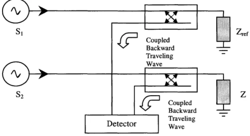
values, an alternative method to the bridge was adopted. The front end design that was used in the final implementation is shown in Figure 14,S, Coupled Ze Backward _ Traveling
O
Wave S2 Z Coupled Backward _ Detecto Traveling Detct I WaveFigure 14. Parallel Directional Coupler Configuration for Measuring Reflection Coefficient
This design employs a parallel configuration of two directional couplers. Two signals are transmitted through the couplers, one of which is transmitted to the active probe (used for taking measurements), while the other is transmitted to a dummy or reference probe. The directional coupler couples the backward traveling wave coming from each of the probe, and the detector uses both the coupled signals to determine magnitude/phase changes in the presence of a load. While this method does not give accurate reflection coefficient values, it allows one to measure changes in
F.
This provides us with sufficient useful information about the load terminating the transmission line, as will be illustrated in the next two chapters when applications are discussed. The dummy probe for a particular application is fixed, and its purpose is to generate a signal for the detector, which would allow the background variations in the system to be subtracted. This can arise due to many factors, such as variations in the generated signal strength, variation in the gain of the amplifier stage over the sweep frequency range, variations in reverse isolation of the directional couplers, etc. It was found that such a differential implementation wassuccessful at removing the natural frequency dependence of the system, giving a much flatter measurement baseline. Such a baseline is extremely important since it acts as the reference when loads are measured. For the tags application in particular, we will see that peak detection is greatly enhanced with a flatter baseline
as well.
For our system, the fact that the DDS is able to produce two output signals of similar magnitude effectively eliminates the need for the front end to produce a reference signal. This simplifies the front-end design considerably when the dual directional-coupler configuration is used. An alternative way of thinking
of this is that since the reference probe is fixed, the frequency dependent reflection coefficient for the reference arm remains the same, thus the magnitude of the backward traveling wave from the reference


![Risiko- & [und] Schutzfaktoren der psychischen Gesundheit humanitärer Einsatzhelfer : eine systematische Literaturübersicht](data:image/gif;base64,R0lGODlhAQABAIAAAP///wAAACH5BAEAAAAALAAAAAABAAEAAAICRAEAOw==)