HAL Id: hal-01315234
https://hal.archives-ouvertes.fr/hal-01315234
Submitted on 13 May 2016
HAL is a multi-disciplinary open access
archive for the deposit and dissemination of
sci-entific research documents, whether they are
pub-lished or not. The documents may come from
teaching and research institutions in France or
abroad, or from public or private research centers.
L’archive ouverte pluridisciplinaire HAL, est
destinée au dépôt et à la diffusion de documents
scientifiques de niveau recherche, publiés ou non,
émanant des établissements d’enseignement et de
recherche français ou étrangers, des laboratoires
publics ou privés.
Low loss GaN waveguides for visible light on Si
substrates
Maksym Gromovyi, F Semond, Jean-Yves Duboz, Guy Feullet, Marc de
Micheli
To cite this version:
Maksym Gromovyi, F Semond, Jean-Yves Duboz, Guy Feullet, Marc de Micheli. Low loss GaN
waveguides for visible light on Si substrates. Journal of the European Optical Society : Rapid
pub-lications, European Optical Society, 2014, J. Europ. Opt. Soc. Rap. Public. 9, 14050 (2014),
�10.2971/jeos.2014.14050�. �hal-01315234�
Low loss GaN waveguides for visible light on Si
substrates
M. Gromovyi
CNRS, CRHEA UP 10, rue Bernard Gregory, 06560 VALBONNE, France
F. Semond CNRS, CRHEA UP 10, rue Bernard Gregory, 06560 VALBONNE, France
J. Y. Duboz CNRS, CRHEA UP 10, rue Bernard Gregory, 06560 VALBONNE, France
G. Feuillet CEA LETI, 17 rue des Martyrs, 38054 Grenoble cedex 9, France
M. P. De Micheli
University Nice Sophia Antipolis, LPMC UMR 7336, Parc Valrose, 06108 Nice cedex 2, France
In this work, we present the fabrication and the characterization of an optical waveguide made of AlN and GaN layers grown by MBE on a Si(111) substrate. For the fundamental mode at 633 nm, the propagation losses are in the order of 2 dB/cm, which is a good number for SC waveguides at this wavelength. The propagation losses dramatically increase with the mode order. A careful comparison of measurements and modeling of the complete structure allows identifying the part of the losses due to absorption in the Si substrate, and showing that propagation losses could be further reduced by using well chosen SOI substrates.
[DOI:http://dx.doi.org/10.2971/jeos.2014.14050]
Keywords: GaN on silicon, GaN on SOI, waveguide losses, visible waveguide, MBE
1 INTRODUC TION
Wide bandgap group III-nitride semiconductors have inter-esting electrooptical properties in the near UV and the visi-ble regions of the spectrum which have led to the successful production of LEDs and laser diodes [1]. In the past decade nonlinear properties of GaN became another subject for in-vestigation. A large transparency window 350 nm–13.6 µm for GaN, which can be extended up to the 200 nm for AlN, makes it possible to implement nonlinear processes such as sum or difference-frequency generation for the wavelength in the visible and UV regions. Second harmonic generation (SHG) based on quasi phase matching by periodical polling was demonstrated for the bulk GaN [2]. Another technique for SHG based on modal dispersion phase matching was shown in GaN planar waveguide grown by MOCVD on sapphire [3]. One important question related to frequency conversion in wavegudes is the integration with other technologies, which leads to the substrate issue. Naturally due to the mature tech-nology and low cost, silicon is the most attractive candidate to which one would prefer to add GaN functionality. Now more and more efforts are done toward integration of GaN into Si technology. In spite of the promising results it still remains a challenge. On the level of fabrication, large lattice param-eters and thermal expansion coefficient mismatch causes the problem of residual stress, defects and cracks. From the opti-cal point of view Si is not a desired material since it absorbs in the visible and the UV. Early developments of the epitaxy (both MBE and MOCVD) of GaN on Si [4,5] have allowed
to solve most problems, so that many devices have been fab-ricated based on GaN grown on Si [6]–[10]. SHG based on modal phase matching was obtained in GaN and AlN micror-ings on Si substrate covered by SiO2insulator [11,12].
The future of integrated GaN photonics dramatically de-pends on the supply of the main building block: low loss GaN waveguides. At the present time there are few publi-cations which discuss GaN based waveguides. These discus-sions mainly address the study of the linear or nonlinear prop-erties of GaN. The losses are generally provided as additional information and the origin of the losses is rarely discussed. The reported losses for visible range are in order of several dB/cm [13,14], and are lower for the telecom 1.55 µm wave-length (<1 dB/cm) [15,16]. In addition, these articles present different fabrication conditions, as well as different measure-ment techniques which leads to a great dispersion of the ex-perimental values.
We believe that the origin of the losses in GaN waveguides is a very important topic which deserves a separate discus-sion and a systematic study. Here we address the influence the waveguide design on the value of the propagation losses in the presence of a Si substrate, this study has not been dis-cussed yet.
In this work we present a GaN on AlN waveguide grown by MBE on Si(111) substrate with 1.9 dB/cm and 3.4 dB/cm
J. Europ. Opt. Soc. Rap. Public.9, 14050 (2014) M. Gromovyi, et al.
losses for the TE0 and TM0 modes respectively at wavelength
λ =632.8 nm. Using theoretical modeling we show that the
absorption in Si can significantly influence the propagation losses of the guided modes. The theoretical model presented below allows to estimate the thickness of AlN layer which is needed for optically isolating the GaN guiding layer from the absorbing Si substrate. We also show that by replacing Si sub-strates by properly chosen SOI subsub-strates one can significantly reduce the losses related to the absorption in Si and obtain a larger flexibility on the choice of AlN buffer layer thickness.
2 E XPERIM ENT
2 . 1 W a v e g u i d e f a b r i c a t i o n
The sample we tested was epitxially grown by ammonia-MBE on a 2” Si(111) wafer. It is composed of a 360 nm AlN buffer grown at 1000◦C on top of which was grown a 1 µm thick GaN layer at 800◦C. Due to a large thermal expansion coefficient mismatch between nitrides and the silicon substrate, nitrides epitaxially grown on silicon are under tensile strain at room temperature and cracks appear if the amount of tensile strain exceeds a certain value. For this sample, layer thicknesses are adjusted in order to decrease as much as possible the wafer bow indicating that the tensile strain is mostly compensated by playing with the lattice mismatch in between GaN and AlN.
We chose a 1 micron thick GaN layer to have enough guided modes at 633 nm to allow a precise characterisation of the re-fractive index profiles of the waveguide with the prism cou-pling technique. Indeed this characterisation method allows deducing refractive indices and thicknesses of the different epitaxial layers constituting the waveguide from the measure-ment of the outcoupling angles for the different modes. The more modes the more precision in the determination of the different parameters. Moreover this thickness is adapted for frequency doubling from 1200 nm to 600 nm.
2 . 2 W a v e g u i d e c h a r a c t e r i z a t i o n
We characterized the waveguide using the prism coupling technique [17] and a HeNe laser at 632.8 nm. We used two ru-tile prisms: the first one for coupling the light into the waveg-uide, and the second one for outcoupling the light from the waveguide and observing M-lines. For 1 µm thick GaN layer
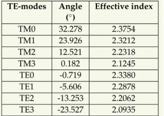
TE-modes Angle Effective index (◦) TM0 32.278 2.3754 TM1 23.926 2.3212 TM2 12.521 2.2318 TM3 0.182 2.1245 TE0 -0.719 2.3380 TE1 -5.606 2.2878 TE2 -13.253 2.2062 TE3 -23.527 2.0935
TABLE 1 Effective indices for the TE and TM modes measured by M-lines technique.
on AlN buffer layer we were able to observe 4 TE and 4 TM modes.
Measuring the outcoupling angles of the different modes, we obtained effective indices of the propagating modes, see Ta-ble1. The value of the effective index for a given mode is determined by the thickness of the guiding layer, and by the refractive indices of the guiding layer and the substrate. In the case of assymmetric step-index planar waveguides, there exist a simple analytical solution which links these quanti-ties [20]. Using these analytical relations and the 8 measured effective indices of the TE and TM modes, we solved the in-verse problem and determined the values of the 5 unknown parameters: ordinary and extraordinary refractive indices of GaN and AlN and the waveguide thickness. The result for the refractive indices of GaN and AlN are presented in Ta-ble2, these values are in a good agreement with previously obtained data [18,19]. As the layers are obtained by MBE the error on their thicknesses are negligible. The errors of the de-termined values of the GaN and AlN refractive indices are coming from the errors made during the measurement of the outcoupling angles. The amplitude of the errors is determined by injecting extreme values in the calculation.
It should be noted that our method gives much better preci-sion for the values of refractive index of GaN than for the AlN index, since only a very small part of the electromagnetic field is confined in the AlN.
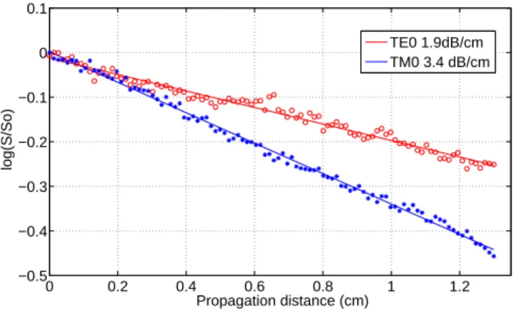
The observation shows that light is locally scattered by some defects and also is more uniformly scattered by the interface roughness. If we assume a uniform scattering rate in the mea-surement area, then the light intensity measured outside the sample is proportional to the light intensity within the guide for a given mode. We chose a region without any defect, and measured the light intensity at different positions along the propagation line. Since 1 µm GaN layer on AlN forms a multi-mode waveguide we tried to measure coupling be-tween modes by observing M-lines with 0-mode being exited. Selectively exciting the TE0 mode it was possible to observe some coupling in the TE1 but the measurements indicate that the intensity coupled into the TE1 mode is at least two orders of magnitude lower than the power present in the TE0 mode. The situation is identical for the TM0 and the TM1 modes, therefore in the following we will neglect this coupling. For the loss measurement we used a highly sensitive, low noise sCMOS camera and the obtained signal was very well match-ing an exponential decay behaviour, see Figure1, giving the losses values 1.9 dB/cm for the TE0 and 3.4 dB/cm for the
λ= 632.8 nm no ne
GaN 2.354 ± 0.001 2.393±0.001 AlN 2.075±0.02 2.117±0.02
∆n 0.279 0.276
TABLE 2 Ordinary and extraordinary refractive indices of GaN and AlN obtained from waveguide characterization. The errors of the determined values of the GaN and AlN refractive indices are coming from the errors made during the measurement of the outcoupling angles. The amplitude of the errors is determined by injecting extreme values in the calculation.
0 0.2 0.4 0.6 0.8 1 1.2 −0.5 −0.4 −0.3 −0.2 −0.1 0 0.1 Propagation distance (cm) log(S/So) TE0 1.9dB/cm TM0 3.4 dB/cm
FIG. 1 Propagation loss estimation for the TE0 and TM0 modes by surface diffusion measurement. Vertical axis gives the logarithm on a base 10 of the ratio between diffused light intensity along the propagation line and diffused light intensity at the starting point, as a function of the propagation distance.
TM0 modes with an uncertainty of ± 0.1 dB/cm, the error of the linear least square approximation. The obtained values indicate that guiding layer are of good quality at this wave-length and present a good potential for device fabrication in the UV and the Visible. Selectively exciting the TE1 or TM1 modes, one can hardly observe the diffusion at the surface af-ter 1 cm of propagation, this distance is even shoraf-ter for higher order modes indicating that, for these modes, the losses reach 20 dB/cm or more.
3 MODELLING
3 . 1 T h e o r e t i c a l m o d e l
To describe the loss mechanism due to the absorption in Si layer, it is not enough to consider a simple three layer model (air/GaN/AlN) for which an analytical solution is known. One has to consider multilayered models which will include Si or SOI substrates into the equations. In the beginning we introduce a theoretical model for the general case of a multi-layered plane waveguide, the scheme of which can be seen in Figure2. We assume that different layers have different phys-ical properties, specifphys-ically different refractive indices. Speak-ing about one separate layer, we are interested in the mod-elling of the wave propagation in uniaxial materials, such as GaN or AlN, with Oz axes associated with an extraordinary refractive index ne, and the Oxy-plane with an ordinary
re-fractive index no. In our model, one given layer has
homoge-neous and isotropic properties in Oxy-plane, and we assume that noand nedo not depend on z-coordinate within the layer.
To describe the losses in the waveguide we allow refractive indices to be complex numbers.
To summarize the above description above in mathematical terms, the dielectric tensor for one layer has the following form: ˆε = εo n2 o 0 0 0 n2o 0 0 0 n2e , (1)
where ε0 is the vacuum permittivity, and no, neare the
ordi-nary and extraordiordi-nary refractive indices. Dielectric tensor is
TE Hz Hx Ey TM Ez Ex Hy
x
z
y
1 2 m . . .FIG. 2 General scheme of a planar multilayered waveguide. The electromagnetic field propagates in the waveguide in x-direction in the form of modes. The modes of the waveguide can be divided into two groups TE-modes, defined by a single y-component of the electric field, and TM-modes – single y-component of the magnetic field.
a piecewise constant function of z-coordinate:
ˆε(z) = ˆε1, 1stlayer, ˆε2, 2ndlayer, . . . . ˆεm, mthlayer. (2)
As it was mentioned above the modes in the planar waveg-uide can be divided into two group TE and TM modes. In the coordinate system displayed on the Figure??, TE modes are described by the next equations:
Ey(x, z, t) = Ey(z) exp(iβx − iωt), TE modes: Hx(x, z, t) = − 1 iωµ0 ∂Ey ∂z , Hz(x, z, t) = 1 iωµ0 ∂Ey ∂x , (3)
where β = kn is the propagation constant along x-direction, n is the effective refractive index of a given mode, k = ω/c is the wave vector in the vacuum.
The system of equations for the amplitude Ey will have the
form: Ey00(z) + k2hn2o(k, z) − n2 i Ey(z) = 0, Ey(z), Ey0(z) − continuous, Ey(±∞) = 0, (4)
where by Ey0 and Ey00 we denote first and second derivatives
with respect to z, no(k, z) is the ordinary refractive index,
which depend on the wave vector k, and also a piecewise con-stant function of the layer with respect to z coordinate. Similarly, the electric and the magnetic fields associated with the TM-modes are give by
Hy(x, z, t) = Hy(z) exp(iβx − iωt), TM modes: Ex(x, z, t) = 1 iωn2 o ∂Hy ∂z , Ez(x, z, t) = − 1 iωn2 e ∂Hy ∂x . (5)
where β = kn is the propagation constant along x-direction, n is the effective refractive index of a given mode, where k = ω/c is the wave vector in the vacuum.
J. Europ. Opt. Soc. Rap. Public.9, 14050 (2014) M. Gromovyi, et al.
GaN 1Μm
AlN 360nm
Si
300Μm
air
TE0
TE1
TE2
TE3
FIG. 3 TE modes profiles.
The equations for the unknown amplitude Hy:
H00y(z) + k2n 2 o(k, z) n2 e(k, z) h n2e(k, z) − n2 i Hy(z) = 0, Hy(z), 1 n2 o(k, z) H0y(z) − continuous, Hy(±∞) = 0. (6)
Eqs. (4) and (6) represent an eigenvalue problems solving which one can find effective indices of TE and TM modes re-spectively. Knowing these effective indices we can estimate the propagation losses. The losses are characterized either by the absorption coefficient α or by propagation losses L:
α = 4π λ Im(n)
h
cm−1i, L = 4.3α hdB cm−1i, (7) where λ is the wavelength, Im(n) - imaginary par of the re-fractive index of a given mode.
3 . 2 S i s u b s t r a t e
To calculate the losses due to the absorption in the Si substrate we consider a 5 layer system: air/GaN/AlN/Si/air. The main advantage of the 5 layers model is that the index of the ex-ternal layers (air) is smaller than the effective indices of the modes we are interested in. This assures that in these layers the fields are evanescent and therefore decay to zero before reaching the edge of the calculation window.
The Si substrate is the only one presenting complex refrac-tive index. The numerical values for the refracrefrac-tive indices at
λ =632.8 nm used in the calculations are taken from Table2
for AlN and GaN and from [21] for Si. Solving the eigen-value problems Eqs. (4) and (6) for multilayered systems is a rather technical procedure, we performed using the Mathe-matica package.
The results of calculations, namely the modes profiles, the modes confinement factors and the losses are presented be-low. Figure3shows the profiles of the TE modes, in addition we calculated the modes confinement factors ηGaNand ηSi:
ηGaN = Energy in GaN layer
Total modal energy , ηSi=
Energy in Si layer Total modal energy, which are listed in Table3.
Using the formulas Eq. (7) we estimated the losses due to the mode energy absorption in Si layer, results are also presented in Table3. The errors range for the modelled losses in Table3
ηGaN ηSi L (%) (%) (dB/cm) TE mode 0 99.5 0.005 1.2±0.3 mode 1 97.6 0.034 9±2 mode 2 93.7 0.21 60±15 mode 3 83.6 1.67 550±150 TM mode 0 99.5 0.009 2.4±0.9 mode 1 97.7 0.08 24±9 mode 2 92.0 0.77 250±100 mode 3 68.6 11.2 >103
TABLE 3 Results of modeling: the confinement factors ηGaN, ηSiand the losses L caused by the absorption in the Si substrate for the different TE and TM modes.
λ= 632.8 nm TE0 TM0
Measured total losses (dB/cm) 1.9±0.1 3.4±0.1 Modelled absorption in Si (dB/cm) 1.2±0.3 2.4±0.9
∆ dB/cm 0.7±0.4 1.0±1.0
TABLE 4 Comparison of the total propagation losses measured during the waveguide characterization with the modeled absorption in the Si substrate.
was determined performing the calculations with the extreme values of the refractive indices from the Table2.
The results of modelling presented in Table3show a natural correlation between the losses and the modal energy confine-ment in the Si layer. The modelling shows that the propaga-tion losses dramatically change with the mode order which corresponds to what have been observed experimentally. At this point it is necessary to recall that measured values rep-resent total losses while we calculate only the absorption in the Si, therefore the difference between these values should represent the influence of the other loss mechanisms: scatter-ing and absorption in the other layers. In Table4we can see that TE0 and TM0 modes present quite different propagation losses while the difference between measured and calculated values are nearly equal. This indicates that the loss variation with polarization is mainly due to the difference of absorp-tion in the Si substrate which directly depends on the confine-ment of two modes. This also indicates that losses due to other mechanisms are in the order of 1 dB/cm.
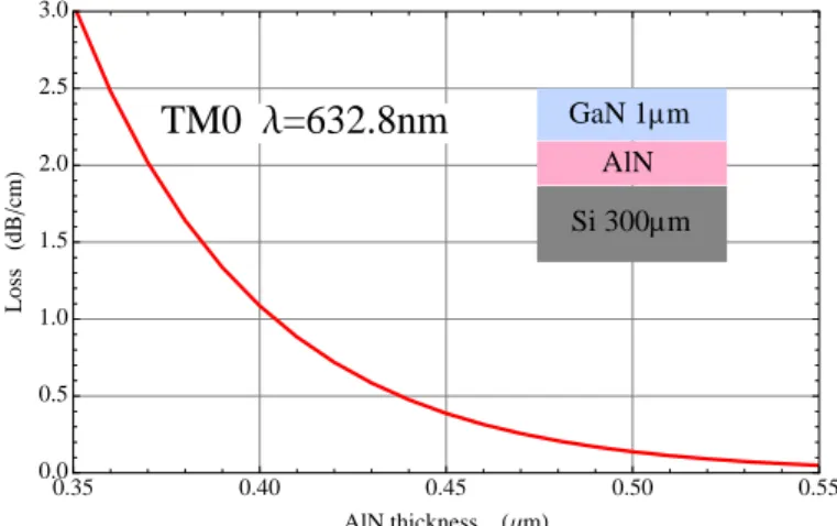
One of the possibilities to reduce the losses due to the absorp-tion in the Si layer is to increase the AlN buffer layer thickness. Figure4shows which thickness of AlN is required to make ab-sorption losses in Si negligible compared to losses due to other mechanisms.
This solution has the disadvantage of inducing very long fab-rication processes since with MBE the speed of growth of AlN is only 0.1 µm/h.
3 . 3 S O I s u b s t r a t e
The second way to reduce the losses is to use SOI substrates. They exist with different designs allowing to reduce the ab-sorption losses by reducing the Si thickness and therefore
GaN 1Ðm AlN Si 300Ðm
TM0 Λ=632.8nm
0.35 0.40 0.45 0.50 0.55 0.0 0.5 1.0 1.5 2.0 2.5 3.0 AlN thickness HΜmL Loss HdB cm LFIG. 4 Modelled absorption for the TM0 mode in the Si substrate as a function of the thickness of the AlN buffer layer.
GaN 1Ðm SiO2 145 nm Si 300Ðm
TM0 Λ=632.8nm
Si 3nm SiO2145 nm Si 3nm SiO21 Ðm AlN Si 16nm 0.15 0.20 0.25 0.30 0.35 0.0 0.1 0.2 0.3 0.4 0.5 0.6 0.7 AlN thickness HΜmL Loss HdB cm LFIG. 5 Losses due to the absorption in the Si layers of SOI substrate for TM0 mode as a function of the thickness of the AlN buffer layer. The solid line corresponds to the structure schematically show on the right part of the figure. Dotted lines represent possible improvement due to the functional Si layer reduction and increasing the thickness of the SiO2layer.
the overlap between the evanescent tail of the mode and the strongly absorbing medium. Figure5demonstrates what can be obtained with different geometries. It should be noted that we cannot eliminate the Si functional layer completely, be-cause it is needed for the epitaxy. Ideally we would like to use SOI with thin (< 10 nm) Si layer and thick (> 1 µm) SiO2
layer. Optimum SOI wafers are not available today, studies are under process to realise them, they will determine the tech-nological limit that we will have to take into account for the realisation of actual devices. Nevertheless, even the structures like Si(16 nm)/SiO2(145 nm) see Figure5, which is
commer-cially available, can significantly reduce the losses due to the absorption in the Si and allow a larger flexibility on the thick-ness of the AlN buffer layer.
4 C ON CL USIO NS
In this work we present a GaN on AlN waveguide grown by MBE on a Si(111) substrate. We fully characterized this waveg-uide in the visible (λ = 632.8 nm) by measuring its index pro-file using the prism coupling technique and the propagation losses of the TE and the TM fundamental modes visualizing the decrease of the scattered light along the propagation line. We obtained values of 1.9 dB/cm and 3.4 dB/cm respectively.
We also performed a carreful modeling of this waveguide, tak-ing into account the full structure and the complex value of the refractive index of the Si substrate at this wavelengh. The comparison between the measured and the calculated values allows to deduce that the difference between the propagation losses of the TE0 and the TM0 modes is perfectly explained by the difference of mode confinement and that the other loss mecanisms are responsible for approximately 1 dB/cm losses. Moreover the modelling allows proposing two possibilities to make the absorption losses negligible compared to the losses induced by other mechanisms: increasing the AlN buffer layer thickness, or using a carrefully chosen SOI substrate.
5 A CK N OW L E D GEM E NT S
We acknowledge support from GANEX (ANR-11-LABX-0014). GANEX belongs to the public funded “Investissements d’Avenir” program managed by the French ANR agency.
Ref er e nc e s
[1] S. Nakamura, and G. Fasol, The blue laser diode: GaN based light
emitters and lasers (Springer, Berlin, 1997).
[2] A. Chowdhury, H. M. Ng, M. Bhardwaj, and N. G. Weimann, “Second-harmonic generation in periodically poled GaN,” Appl. Phys. Lett.83, 1077–1079 (2003).
[3] D. N. Hahn, G. T. Kiehne, J. B. Ketterson, G. K. L. Wong, P. Kung, A. Saxler, and M. Razeghi, “Phase-matched optical second-harmonic generation in GaN and AlN slab waveguides,” J. Appl. Phys.85, 2497–2500 (1999).
[4] F. Semond, Y. Cordier, N. Grandjean, F. Natali, B. Damilano, S. Vézian, and J. Massies. “Molecular beam epitaxy of group-III ni-trides on silicon substrates: growth, properties and devices appli-cations,” Phys. Status Solidi A188, 501–510 (2001).
[5] E. Feltin, B. Beaumont, M. Laugt, P. De Mierry, P. Vennegues, H. Lahreche, M. Leroux, et al., “Stress control in GaN grown on silicon (111) by metalorganic vapor phase epitaxy,” Appl. Phys. Lett.79, 3220 (2001).
[6] J. Y. Duboz, J. L. Reverchon, D. Adam, B. Damilano, F. Semond, N. Grandjean, and J. Massies “High performance solar blind detec-tors based on AlGaN grown by MBE on Si,” Phys. Status Solidi A188,
325–328 (2001).
[7] F. Semond, P. Lorenzini, N. Grandjean, and J. Massies“High electron mobility AlGaN/GaN heterostructures grown on Si(111) by molecular beam epitaxy,” Appl. Phys. Lett.82, 335 (2001).
[8] S. Dalmasso, E. Feltin, P. De Mierry, B. Beaumont, P. Gibart, and M. Leroux, “Green electroluminescent (Ga,InAl)N LEDs grown on Si(111),” Electron. Lett.36, 1728–1730 (2000).
[9] A. Krost, and A. Dadgar “GaN-Based Devices on Si,” Phys. Status Solidi A194, 361–375, (2002).
[10] E. V. Lutsenko, V. N. Pavlovskii, V. Z. Zubialevich, A. I. Stognij, A. L. Gurskii, and V. A. Hryshanau, “Growth, stimulated emission, photo-and electroluminescence of InGaN/GaN EL-test heterostructures,” Phys. Status Solidi A0, 272–275 (2002).
[11] C. Xiong, W. Pernice, K. K. Ryu, C. Schuck, K. Y. Fong, T. Palacios, and H. X. Tang “Integrated GaN photonic circuits on silicon (100) for second harmonic generation,” Opt. Express19, 10462–10470 (2011).
J. Europ. Opt. Soc. Rap. Public.9, 14050 (2014) M. Gromovyi, et al.
[12] W. H. P. Pernice, C. Xiong, C. Schuck, and H. X. Tang “Second har-monic generation in phase matched aluminum nitride waveguides and micro-ring resonators,” Appl. Phys. Lett.100, 223501 (2012).
[13] E. Doghèche, D. Rémiens, A. Boudrioua, and J. C. Loulergue “Growth and optical characterization of aluminum nitride thin films deposited on silicon by radio-frequency sputtering,” Appl. Phys. Lett.74, 1209 (1999).
[14] H. P. D. Schenk, E. Feltin, M. Laügt, O. Tottereau, P. Vennéguès, and E. Doghèche “Realization of waveguiding epitaxial GaN layers on Si by low-pressure metalorganic vapor phase epitaxy,” Appl. Phys. Lett.83, 5139 (2003).
[15] R. Geiss, A. Chowdhury, C. M. Staus, H. M. Ng, S. S. Park, and J. Y. Han, “Low loss GaN at 1550 nm,” Appl. Phys. Lett.87, 132107
(2005).
[16] A. Stolz, E. Cho, E. Doghèche, Y. Androussi, D. Troadec, D. Pavlidis, and D. Decoster “Optical waveguide loss minimized into gallium nitride based structures grown by metal organic vapor phase epi-taxy,” Appl. Phys. Lett.98, 161903 (2011).
[17] P. K. Tien, and R. Ulrich, “Theory of prism-film coupler and thin-film light guides,” J. Opt. Soc. Am.60, 1325–1337 (1970).
[18] U. Ozgur, G. Webb-Wood, H. O. Everitt, F. Yun, and H. Morkoc, “Sys-tematic measurement of AlxGa1-xN refractive indices,” Appl. Phys.
Lett.79, 4103–4105 (2001).
[19] S. Pezzagna, J. Brault, M. Leroux, J. Massies, and M. de Micheli, “Refractive indices and elasto-optic coefficients of GaN studied by optical waveguiding,” J. Appl. Phys.103, 123112 (2008).
[20] A. Yariv, Quantum Electronics (Wiley, New York, 1975).
[21] E. D. Palik (ed.), Handbook of optical constants of solids (Aca-demic Press, San Diego, 1998).

![Risiko- & [und] Schutzfaktoren der psychischen Gesundheit humanitärer Einsatzhelfer : eine systematische Literaturübersicht](data:image/gif;base64,R0lGODlhAQABAIAAAP///wAAACH5BAEAAAAALAAAAAABAAEAAAICRAEAOw==)