HAL Id: tel-03135075
https://tel.archives-ouvertes.fr/tel-03135075
Submitted on 8 Feb 2021HAL is a multi-disciplinary open access
archive for the deposit and dissemination of sci-entific research documents, whether they are pub-lished or not. The documents may come from teaching and research institutions in France or abroad, or from public or private research centers.
L’archive ouverte pluridisciplinaire HAL, est destinée au dépôt et à la diffusion de documents scientifiques de niveau recherche, publiés ou non, émanant des établissements d’enseignement et de recherche français ou étrangers, des laboratoires publics ou privés.
Victor Fan Arcara
To cite this version:
Victor Fan Arcara. Tunnel junctions in nitride heterostructures for optoelectronic applications. Optics [physics.optics]. Université Côte d’Azur, 2020. English. �NNT : 2020COAZ4010�. �tel-03135075�
Jonctions tunnel dans les hétérostructures
des matériaux nitrures pour applications
optoélectroniques
Victor FAN ARCARA
(1) CEA/LETI : 17 Avenue des Martyrs, Grenoble
(2) CNRS/CRHEA : Rue Bernard Grégory, Valbonne
Présentée en vue de l’obtention du grade de docteur en physique d’Université Côte d’Azur
Dirigée par : Guy Feuillet (1), directeur
de recherche
Co-dirigée par : Jean-Yves Duboz (2),
directeur de recherche
Co-encadrée par : Benjamin
Damilano (2), chargé de recherche
Soutenue le : 10/03/2020
Devant le jury, composé de : Rapporteurs
Maria Tchernycheva, Directrice de Recherche,
CNRS – Université Paris Sud, France
Nicolas Grandjean, Professeur, EPFL, Suisse Examinateurs
Armin Dadgar, Professeur,
Otto-von-Guericke-Universität Magdeburg, Allemagne
Eva Monroy, Directrice de Recherche, IRIG CEA -
Université Grenoble Alpes, France
Jean Paul Salvestrini, Professeur, Georgia Tech
Lorraine, France
NT LOGO
CO-TUTELLE ÉVENTUELLE
Les jonctions tunnel apportent une solution alternative aux problèmes qui limitent l'efficacité des diodes électroluminescentes émettant dans l’ultraviolet, notamment la forte résistivité des couches d’AlGaN dopées p et la mauvaise injection de trous qui en résulte. L’objectif de cette thèse est l'optimisation des structures LED à jonction tunnel à base de GaN et d’AlGaN et leurs caractérisations structurales et optoélectroniques. La croissance d'une LED à JT entièrement par MOCVD est attrayante sur le plan industriel, mais les couches de (Al)GaN dopées p développées par cette technique souffrent de la repassivation des accepteurs de Mg par l’hydrogène présent dans la chambre de croissance. Nous avons essayé et réussi à minimiser ce problème en modifiant les conditions de croissance de la jonction tunnel. Des résultats positifs ont été atteints sur des LED bleues, notamment avec des jonctions tunnel GaN comprenant une couche intercalaire en InGaN qui augmente sa transparence tunnel. Cependant, ce procédé tout MOCVD semble délicat à optimiser et son extension aux matériaux AlGaN difficile. Grâce à une approche de croissance hybride MOCVD+MBE, des couches de GaN et d'AlGaN dopées p peuvent être obtenues avec des accepteurs Mg actifs tout en profitant des régions actives de haute qualité fournies par le MOCVD. Avec un JT hybride à base de GaN, nous avons pu obtenir, aussi bien avec le Si qu’avec le Ge, des niveaux de dopage n++ plus élevés, que ceux des JT MOCVD, ce qui a permis de réduire considérablement la tension de fonctionnement des dispositifs. Le fort dopage Ge des couches de GaN a permis d'obtenir des densités électroniques de l’ordre de 5x1020cm-3 avec des mobilités et des résistivités à l’état de l’art, sans introduire
une forte contrainte dans le réseau. Dans la deuxième partie de ce travail, nous avons développés des JT à base d’AlGaN dopées Ge sur des LEDs UV en modifiant progressivement leur concentration d’Al jusqu'à une valeur de 70 %. Dans la gamme des UV, les JT deviennent d'une importance capitale en augmentant l'efficacité de l'injection sans compromettre l'extraction de la lumière. Des forts niveaux de dopage Ge ont été obtenus conduisant à des jonctions fines comme le montre l’holographie électronique. Même si les chutes de tension introduites par l'utilisation des JT restent notables (quelques volts), l’injection de trous hors équilibre permet une augmentation significative de l’efficacité d’injection dans la LED conduisant ainsi à une forte augmentation de l'efficacité quantique des dispositifs.
Mots clés : jonctions tunnel, croissance hybride, dopage germanium, ingénierie de la polarisation, nitrure de gallium, nitrure de gallium d'aluminium.
Tunnel junctions provide an alternative solution to issues that limit the efficiency of ultraviolet light emitting diodes, such as the high resistivity of p-doped AlGaN layers and the resulting poor hole injection. The objective fo this thesis is the optimization of GaN and AlGaN based tunnel junction LED structures and their structural and optoelectronic characterization. The growth of a JT LED entirely by MOCVD is industrially appealing, but the p-doped (Al)GaN layers developed by this technique suffer from the repassivation of the Mg acceptors by the hydrogen present in the growth chamber. We have tried and succeeded to minimize this problem by modifying the growth conditions of the tunnel junction. Positive results have been achieved on blue LEDs, in particular with GaN tunnel junctions including an InGaN interlayer that increases its tunnel transparency. However, this all MOCVD process seems difficult to optimize and its extension to AlGaN materials difficult. Thanks to a hybrid MOCVD+MBE growth approach, p-doped GaN and AlGaN layers can be obtained with active Mg acceptors while taking advantage of high quality active regions provided by MOCVD. With a GaN-based hybrid JT, we have been able to obtain, with both Si and Ge, higher levels of n++ doping than those of the MOCVD JTs, thus significantly reducing the operating voltage of the devices. The strong Ge doping of the GaN layers allowed us to obtain electron densities of the order of 5x1020cm-3 with state-of-the-art mobilities and resistivities, without introducing
a strong constraint in the network. In the second part of this work, we have developed AlGaN-based JTs doped with Ge on UV LEDs by gradually changing their Al concentration up to a value of 70%. In the UV range, the JTs become of paramount importance by increasing the injection efficiency without compromising light extraction. High levels of Ge doping have been obtained leading to thin junctions as shown by electronic holography. Even if the voltage drops introduced by the use of JTs remain significant (a few volts), the injection of out-of-equilibrium holes allows for a significant increase of the injection efficiency in the LED leading to a strong increase of the quantum efficiency of these devices.
Keywords: tunnel junctions, hybrid growth, germanium doping, polarization engineering, gallium nitride, aluminum gallium nitride.
“The dreamers may die, but the dreams live on”
To my parents, my grandparents Maria do Carmo
and Lestychildes and to my loving wife.
List of tables ... xi
List of figures ... xii
1. Introduction ... 17
2. Blue and UV LEDs: fundamentals and issues ... 22
2.1. Basic LED functioning ... 22
2.1.1. Radiative and non-radiative recombination ... 24
2.1.2. Quantum wells ... 26
2.1.3. The different contributions to LED efficiency ... 28
2.2. III-N materials for LED applications ... 29
2.2.1. Wurtzite structure and spontaneous polarization ... 30
2.2.2. Lattice parameters in (Al,Ga)N and the choice of a substrate ... 31
2.2.3. Piezoelectric field in nitride heterostructures ... 34
2.2.4. Band structure and symmetry of the valence band ... 37
2.3. UV light sources ... 38
2.3.1. Present day UV lamps for sterilization ... 39
2.3.2. UV LEDs ... 41
2.3.2.1. Current state of UV-B and UV-C LEDs ... 42
2.3.2.2. Obstacles for the External quantum efficiency of UV LEDs ... 44
Internal quantum efficiency issue ... 44
Injection efficiency issue ... 47
Extraction efficiency issue ... 49
3. Tunnel Junctions ... 56
3.1. Historical overview ... 56
3.2. Tunnel junctions in forward bias (Esaki diode) ... 58
3.3. Tunnel junction in reverse bias ... 60
3.4. Derivation of the tunnel current ... 62
3.4.1. Interband tunneling ... 63
3.4.1.1. Kane’s approach ... 64
3.5.1.Mg doping ... 74
3.5.2.Si doping ... 746
3.5.3.Ge doping ... 78
3.6. State of the art of nitride tunnel junctions in light emitters ... 80
3.6.1.Visible devices ... 80
3.6.2.UV LEDs with Tunnel Junctions ... 86
4. All-MOCVD Tunnel junctions ... 94
4.1. Principles of MOCVD growth ... 94
4.1.1. Growth parameters ... 95
4.1.2. Passivation of Mg acceptors ... 97
4.2. Tunnel junctions grown at low temperature and high growth rate ... 99
4.2.1. Morphological and compositional analyses ... 102
4.2.2. Electron-holography TEM analysis ... 107
4.2.3.Optoelectronic properties ... 108
4.3. Lateral degassing treatment ... 111
Conclusion ... 114
5. Hybrid tunnel junctions ... 118
5.1. The hybrid growth method ... 118
5.1.1. Overview of MBE growth ... 119
5.1.2. Regrowth interface ... 121
5.2. Hybrid Si n-doped tunnel junctions on blue InGaN/GaN LEDs ... 123
5.2.1. Morphological and compositional analyses ... 126
5.2.2. Electron-holography TEM analysis ... 128
5.2.3.Optoelectronic properties ... 129
5.3. Doping reproducibility of Si in NH3 assisted MBE ... 132
5.4. Hybrid Ge n-doped tunnel junctions on blue InGaN/GaN LEDs ... 137
5.4.1. Feasibility of n++ GaN:Ge ... 138
5.4.2. Morphological and compositional analyses ... 139
5.4.3. EDX / Electron-holography TEM analyses ... 143
5.5.1.1. Morphological and compositional analyses ... 149
5.5.1.2.EDX / Electron-holography TEM analyses ... 151
5.5.1.3. Optoelectronic properties ... 153
5.5.2. Al0.5Ga0.5N tunnel junctions on 303nm emission AlGaN LEDs ... 156
5.5.2.1. Morphological and compositional analyses ... 157
5.5.2.2.EDX / Electron-holography TEM analyses ... 159
5.5.2.3.Optoelectronic properties ... 162
5.5.3. Al0.7Ga0.3N tunnel junctions on 289nm emission AlGaN LEDs ... 167
5.5.3.1. Morphological analysis ... 169
5.5.3.2. Optoelectronic properties... 170
Conclusion ... 173
List of tables
Table 2-1. Lattice parameters of GaN and AlN and their thermal expansion
coefficients ...31
Table 2-2 : Parameters of the most used substrates for the growth of GaN et Al(Ga)N alloys...32
Table 2-3 : Calculated piezoelectric coefficients of (Al,Ga,In)N ...35
Table 2-4 : Properties of the most used commercially available Hg lamps ...39
Table 2-5 : Current state of the art on optical powers of UV-B and C LEDs ...43
Table 3-1: Summary of the literature on blue LEDs with tunnel junctions ...84
Table 3-2: Summary of the literature on UV LEDs with tunnel junctions. ...89
Table 4-1: Si concentrations in all the MOCVD TJs as deduced from SIMS analysis ...106
List of figures
Figure 2-1: PN junctions at equilibrium. a) Without bias; b) Space charge region;
c) Under bias. ... 24
Figure 2-2: Radiative and non-radiative recombinations. a) Auger; b) Shockley-Read-Hall; c) deep level transition and d) band edge emission. Adapted from Schubert, 2006. ... 25
Figure 2-3: Bandgap energy (eV) by in plane a lattice parameter (nm) for (Al,In,GaN)N systems. ... 29
Figure 2-4: a) Wurtzite GaN structure; b) Spontaneous polarization by lattice parameter u. Adapted from Wood et Jena. ... 31
Figure 2-5: Electric field discontinuity by Al content in AlGaN/GaN heterojunction active region. Adapted from Matta et al. ... 36
Figure 2-6: Electronic band structures of a)GaN and b)AlN. ... 37
Figure 2-7: Valence band splitting of a) GaN and b) AlN. The possible excitons related to holes coming from these subband levels are marked in red. ... 38
Figure 2-8. UV-C light emission peaks of (a) low pressure and (b) medium pressure Hg lamps. Adapted from ‘Aquafine’ website. ... 40
Figure 2-9. Potential applications for UV sources. ... 41
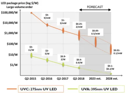
Figure 2-10. LED package price, in $ per Watt, throughout the last years. ... 43
Figure 2-11. External quantum efficiency by the wavelength of emission. ... 44
Figure 2-12. Simulated IQE vs dislocation density curves for an AlGaN MQW LED ... 47
Figure 2-12. Dependence of the activation energy of Mg acceptors on the Al content. ... 48
Figure 2-14. a) Photoluminescence spectra showing the change in polarization of the emitted light in high Al content AlxGa1-xN; b) Schematic of an AlGaN LED and the escape cone, polarized perpendicular to c. ... 50
Figure 3-1 : Band diagram of a degenerated p-n junction in thermal equilib.. ... 59
Figure 3-2: Simplified energy band diagrams and IV-curves of a tunnel diode at a) zero bias; b) bias approaching the peak of the curve; c) bias after the peak approaching the valley and d) bias after the valley. Adapted from Sze. ... 60
Figure 3-3: a) IV curve at negative bias; b) Simplified band diagram of a tunnel diode at negative bias. Adapted from Sze. ... 61
Figure 3-4: Sketch of the out-of-equilibrium hole generation through interband tunneling on a degenerately doped TJ-LED under reverse bias. ... 62
Figure 3-6: Simplified band diagrams to compare the electric field introduced by an interlayer. a) GaN inserted between undoped AlGaN layers; b) n-AlGaN
grown on p-AlGaN ... 67
Figure 3-7 : Band bending on a) tunnel homojunctions and b) interlayer tunnel junctions. Adapted from Zhang. ... 68
Figure 3-8: Simulated I-V curve for an n-Al0.4Ga0.6N / GaN (2nm) / p-Al0.4Ga0.6N tunnel junction varying the n-doping levels. ... 72
Figure 3-9: Simulated curves for n-AlGaN/interlayer/p-AlGaN tunnel junctions. While the n-doping level remains at 4x1020cm-3, major parameters are varied within the calculation: thicknesses of the undoped (a) and doped(b) GaN interlayers and Al content in the AlxGa1-xN tunnel junction p-n layers (c). A TJ Al0.4Ga0.6N diode with an InGaN interlayer is put under a 0.4V bias (d). The In content is varied from 0 to 30%. ... 73
Figure 3-10: Acceptor ionization energy versus acceptor concentration NA. Adapted from Brochen et al. ... 75
Figure 3-11: Evolution of the free hole concentration (p) and resistivity (ρ) with the Al content x in Mg-doped AlxGa1-xN alloys. Adapted from Razeghi et al. .... 76
Figure 3-12: Si donor activation energy versus the Al content x in AlxGa1-xN alloys. Adapted from Pearton. ... 77
Figure 3-13: Evolution of the carrier concentration and resistivity by Al mole fraction in Ge-doped AlGaN alloys. Adapted from Blasco et al. ... 80
Figure 4-1: Precursors most used in the MOCVD growth of III-Ns. a) Trimethyl (Al, In, Ga), where M is the metallic compound; b) Triethylgallium; c) Ammoniac. ... 95
Figure 4-2: Grown stacks of MOCVD tunnel junctions with different growth parameters. In green tones are the layers grown using the showerhead reactor, and in blue the home-made vertical reactor. ... 100
Figure 4-3: SEM images of a) TJ-A, b) TJ-B and c) TJ-C. ... 103
Figure 4-4: AFM images of a) S-LED, b)TJ-C and c) TJ-D. ... 104
Figure 4-5: SIMS analysis of a) TJ-A and b) TJ-B. ... 105
Figure 4-6: Electron holography TEM images. (a), (b) and (c) are the STEM and phase images and the potential profile of TJ-A, respectively. (d), (e) and (f) are respectively the STEM and phase images and the potential profile of TJ-B. .. 107
Figure 4-7: Images of the top surface electroluminescence of the light emitting diodes at 1 mA. TG corresponds to the growth temperature of the n-GaN grown on top of the blue light emitting diode structures. ... 108
Figure 4-8: Current density versus voltage (a) and Differential resistance versus current density (b) curves of S-LED, TJ-A and TJ-B. ... 109
Figure 4-9: Optical power versus current (a) and External Quantum Efficiency versus current (b) curves of S-LED, TJ-A and TJ-B. ... 111 Figure 4-10: Chart flow of the entire growth and degassing processes... 112 Figure 4-11: Current density versus voltage (a) and Optical power versus current
(b) for TJs A, At, B and Bt. ... 114 Figure 5-1: MBE growth chamber. ... 120 Figure 5-2: Growth stacks of (a) reference LED (S-LED) and (b) hybrid Si-doped
TJ (HTJ-A) ... 125 Figure 5-3: AFM images of (a) S-LED and (b) HTJ-A ... 126 Figure 5-4: SIMS analysis of HTJ-A. ... 128 Figure 5-5: Electron holography TEM images. (a), (b) and (c) are the STEM and
phase images and the potential profile of HTJ-A, respectively. ... 128 Figure 5-6: Light emission from a) TJ-B and b) HTJ-A under a current of 5mA for (300x300) µm2 LEDs ... 130
Figure 5-7: (a) JV curves and (b) Differential resistance of HTJ-A in comparison to the reference S-LED and the MOCVD TJs (TJs A and B) ... 131 Figure 5-8: Current density versus (a) optical power and (b) EQE of HTJ-A in
comparison to the reference S-LED and the MOCVD TJs (TJs A and B). ... 132 Figure 5-9: Growth stacks of S-LED* (a) and HTJ-B (b). ... 134 Figure 5-10: AlxGaN (300x300) µm2 LEDs under an applied current of 10mA. (a)
x=0.05; (b) x=0.15. ... 134 Figure 5-11: (a) Current density of the (300x300) µm2 AlGaN TJ LEDs and their
references. (b) Comparison between Al0Ga1N TJ and the HTJ-A, both
possessing the same growth stacking. ... 135 Figure 5-12: Si doping levels as a function of the temperature of the Si cell. ... 136 Figure 5-13: Growth stack of HTJ-B. ... 137 Figure 5-14: Hall effect measurements of free electron concentration and beam
equivalent pressure versus Ge cell temperature for Ge-doped GaN epilayers grown by MBE. ... 139 Figure 5-15: AFM images of (a) S-LED and (b) HTJ-B. ... 140 Figure 5-16: SIMS analysis of HTJ-B. ... 141 Figure 5-17: a) Atom probe 3D reconstruction of HTJ-B by a volume of 40 × 40 ×
100 nm3 around the TJ. Only 24Mg2+ ions, in red, and 74Ge2+ ions, in blue, are
depicted. b) Concentration of dopants through the APT-SIMS analysis.29 ... 142
Figure 5-18: Simulations of the band diagram around the Γ point at the tunnel junction level using values detected by APT-SIMS method and nominal values.29 ... 143
Figure 5-19: Electron-holography TEM analysis of HTJ-B. (a) HAADF STEM, (b) Phase Image and (c) Potential profile along the distance. (d), (e) and (f) show the EDX analysis for Al, In and Ge elements, while (g) focuses on the Ge
profile along the tunnel junction obtained by EDX. ... 144 Figure 5-20: Current density vs voltage (a) and optical power (b) of HTJ-B in
comparison to S-LED. Inset of (b) shows a (300x300) µm2 HTJ-B LED under a
current injection of 5mA. ... 146 Figure 5-21: Growth stacks of (a)S-DH and (b)HTJ-C. ... 149 Figure 5-22: AFM images of (a) (10x10)µm2 and (b) (2x2)µm2 scans of S-DH. The
(10x10)µm2 and (2x2)µm2 scans of HTJ-C are shown at (c) and (d) respectively.
... 150 Figure 5-23: SIMS analysis of HTJ-C at the tunnel junction level ... 151 Figure 5-24: Electron-holography TEM analysis of HTJ-C. (a) HAADF STEM, (b)
Phase Image and (c) Potential profile along the depth of the sample. (d) and (e) show the EDX analysis for Al and Ga, respectively. ... 152 Figure 5-25: Backside emission room temperature CW electroluminescence peaks of HTJ-C. Inset: picture of a (60x60) µm2 LED under a voltage of 20mA. ... 154
Figure 5-26: Current density versus voltage (a) and optical power (b) for S-DH and HTJ-C LEDs. ... 155 Figure 5-27: Growth stacks of (a) S-UVLED; (b) HTJ-D and (c) HTJ-E. ... 157 Figure 5-28: AFM (10x10) µm2 scans of (a) S-UVLED and (b) HTJ-D. A (2x2) µm2
scan of HTJ-D is shown at (c). ... 158 Figure 5-29: SIMS analysis of (a) HTJ-D and (b) HTJ-E ... 158 Figure 5-30: Electron holography TEM analysis of the TJ without interlayer
(HTJ-D). (a) HAADF STEM, (b) Phase Image and (c) Potential profile along the depth of the sample. (d) and (e) show the EDX analysis for Al and Ge, respectively... 160 Figure 5-31: Transmission electron microscopy of HTJ-E (a) BF-STEM; (b)
HAADF-STEM; (c) phase image and (d) phase profile ... 161 Figure 5-32: EDX mapping of HTJ-E of different elements through coupling with
different STEM techniques. (a) Al from HAADF STEM and (b) from HRSTEM; (c) Ge from HAADF STEM and (d) from HRSTEM; and (e) Ga from HAADF STEM and (f) from HRSTEM. ... 162 Figure 5-33: Room temperature CW electroluminescence measurement of HTJ-D. Inset shows a (40x40) µm2 LED under operation at 5mA. ... 163
Figure 5-34: Current density versus voltage (a) and differential resistance (b) of S-UVLED, HTJ-D and HTJ-E. ... 165 Figure 5-35: Current versus optical power (a) and EQE (b) of S-UVLED, HTJ-D
and HTJ-E. ... 166 Figure 5-36: Growth stacks of (a) HTJ-F, (b) HTJ-G, (c) HTJ-H and (d) HTJ-I. . 168
Figure 5-37: AFM 10x10 µm2 scans of (a) HTJ-F, (b) HTJ-G, (c) HTJ-H and (d)
HTJ-I. The 2x2 µm2 of the same samples are shown respectively at (e), (f), (g)
and (h). ... 169 Figure 5-38: Micrographs of (a) HTJ-F, (b) HTJ-G, (c) HTJ-H and (d) HTJ-I. ... 170 Figure 5-39: Room temperature CW electroluminescence measurement of (a)
HTJ-F and (b) HTJ-G. Inset of (b) shows a (60x60) µm2 LED under operation
at 5mA. ... 171 Figure 5-40: Current density versus voltage (a) and differential resistance (b) of
HTJ-F and HTJ-G. ... 172 Figure 5-41: Current density versus optical power (a) and external quantum
CHAPTER 1
Introduction
One does not need to exhaust her/himself to find arguments in the literature that can endorse that III-nitrides semiconductor materials, since their discovery, have revolutionized the world of electronics and optoelectronics. Quaternary, ternary and binary compounds made from these elements can cover all of the visible and part of the ultraviolet and infrared spectra of light in light-emitting-diodes (LEDs), being frequently used in transistors and photovoltaic cells too. Even though these latter two are also extremely relevant to society nowadays, this thesis will focus only on the brightest: the LEDs.
The first report of a light-emitting-diode dates back to 1907, when Henry Round, working for Marconi labs, applied a voltage of 10V to a SiC crystal and noticed the emission of a ‘yellowish’ light. This discovery was however put on ‘standby’ for two decades, being resumed by Oleg Losev in 1927 in soviet Russia, who published the first working theory. He then kept studying the phenomena of electroluminescence in SiC and other semiconductors. Many other researchers resumed Losev’s work, but the first patent of an LED would only be published in 1961 for the first infrared LED, while the first visible LED (red) was patented on the next year by Nick Holonyak from General Electric.1–4 Along with Holonyak’s
discovery, the materials advances made by Akasaki and Amano in the field of III-nitride semiconductors and the first blue LED reported by Nakamura in 1994 revolutionized solid-state lighting.5–8
Applications for these III-nitride diodes can be found in almost every wavelength emitted by a III-V LED, but not all of them perform at the same level. Familiar examples come to our minds, such as the famous drop in performance of green LEDs (also known as “the green gap”)9 and the low efficiency of UV emitting
structures (still without a name but not less challenging than the previous). Several efforts and decades of studies have been made in order to treat these two common issues in semiconductor optoelectronic devices, especially for UV diodes.
The high demand for UV sources gives rise to the market of UV LEDs and Hg lamps. These latter are currently supplying most of the market needs, corresponding to 95.4% of the total UV sources market in 2014, with the role of UV LEDs expected to grow to only 4.9% in 2020.10 This difference in market share
exists even though mercury lamps present short lifetimes, bulky designs, and can only emit at fixed wavelengths.11 Not to mention the Hg related hazard which
could someday lead to a full banishment of Hg lamps.
The reason for this is linked to a steep decrease in efficiency with decreasing wavelength for deep-UV LEDs, which in turn is due to other several reasons, and all of them will be discussed in Chapter 2 along with some fundamentals of LEDs (basic functioning, efficiency, charge confinement, and, an overview of UV LEDs, with their applications and challenges). This chapter will also cover the properties of (Al,Ga,In)N materials which are commonly used for these applications.
The interest in helping to change this scenario for UV LEDs motivated this thesis, made possible through funding from GaNeX, a French network of laboratories working on GaN, and from a project funded by the French National
Research Agency (ANR). The goal of this project, called DUVET (‘Diodes UltraViolet à Effet Tunnel’ in French), was to develop efficient tunnel junctions which would then be coupled to UV emitters. These tunnel junctions are heavily-doped semiconductor pn junctions that could help increase efficiency in UV LEDs, and their functioning principles will be thoroughly explained in Chapter 3 along with simulations performed by our group on tunneling currents on AlGaN diodes. This chapter will also contain a review of the literature on tunnel junctions used for blue and UV LEDs.
In order to synthesize these tunnel junctions for UV, it was decided that the project would firstly focus on finding an adequate growth method suited to blue LEDs. Devices emitting in this wavelength were chosen because they were already known and grown in the CRHEA (Centre de Recherche sur l’Hétéro-Epitaxie et ses applications) laboratory, which was the main working site for this project due to its know-how in the epitaxial growth of semiconductors and the easily-accessible clean room facilities. The other main actor in DUVET was the CEA/LETI (Comissariat à l’énergie atomique et aux énergies alternatives/ Laboratoire d’électronique des technologies de l’information), a laboratory in which more advanced characterizations could be performed, such as holographic TEM and Atom Probe Tomography.
The first growth method tried in our project was the Metalorganic Chemical Vapor Deposition, or MOCVD. This is the industry’s choice for the growth of commercial blue LEDs. Tunnel junctions were grown on top of blue LEDs in a full MOCVD approach. However, all MOCVD LEDs with tunnel junctions suffer from the repassivation of Mg acceptors, reducing the ionized
p-dopants and drastically reducing the performance of the device. In order to tackle his issue, we have adapted the growth conditions to reduce this repassivation. In addition, we have performed a lateral degassing treatment to activate the Mg acceptors, and all these results are shown in Chapter 4, also including a quick explanation of this growth method.
We have then tried a new approach based on the satisfying results obtained in the literature – a hybrid approach, counting on the growth of the LED and part of the tunnel junction by MOCVD followed by the use of a Molecular Beam Epitaxy (MBE) reactor to grow the rest of the tunnel junction. This latter method of epitaxy, here made with the help of ammonia, can synthesize high quality layers under vacuum, and achieve high doping levels which are essential to the correct performance of tunnel junctions. This growth method showed promising results from the first try, being able to considerably reduce the operating voltages of our tunnel junction LEDs, and was then chosen as the main growth technique for the upper n++ part of the tunnel junction.
After choosing the growth method, we came across a technical issue related to NH3-MBE growth of highly Si-doped layers. This obstacle was critical for the
thesis, as it would cause a change in the n-dopant used for our tunnel junctions – from Si to Ge, based on recent results obtained in the literature. After this issue was seen to, we then proceeded to growing LEDs and TJs with more and more Al in order to move towards UV- C sources. We grew tunnel junctions on UV-B (316 and 300nm) and UV-C (289nm) emitting structures made in CRHEA. The results of the characterization of all hybrid tunnel junction LEDs are given in Chapter 5, which contains additionally an overview on MBE.
References
1 ‘History of LEDs’:
http://www.historyoflighting.net/light-bulb-history/history-of-led/.
2
https://www.electronics-notes.com/articles/history/light-emitting-diode-led/led-history.php
3 O.V. Lossev, Lond. Edinb. Dublin Philos. Mag. J. Sci. 6, 1024 (1928). 4 N. Holonyak and S.F. Bevacqua, Appl. Phys. Lett. 1, 3 (1962).
5 H. Amano, N. Sawaki, I. Akasaki, and Y. Toyoda, 4 (1985).
6 S. Nakamura, T. Mukai, and M. Senoh, Appl. Phys. Lett. 64, 1687 (1994). 7 S. Nakamura, T. Mukai, M. Senoh, and N. Iwasa, Jpn. J. Appl. Phys. 31, L139
(1992).
8 J.Y. Tsao, M.H. Crawford, M.E. Coltrin, A.J. Fischer, D.D. Koleske, G.S.
Subramania, G.T. Wang, J.J. Wierer, and R.F.K. Jr, 29 (2014).
9 M.H. Crawford, IEEE J. Sel. Top. Quantum Electron. 15, 1028 (2009).
10 Global UV LED Market (2018-2023), 2018 report sample, Mordor Intelligence. 11 Y. Muramoto, M. Kimura, and S. Nouda, Semicond. Sci. Technol. 29, 084004
CHAPTER 2
Blue and UV LEDs: fundamentals and issues
As rapidly presented in the introduction, our work consisted in first implementing Tunnel Junctions in visible LEDs, and then moving to UV-LEDs in order to address some of the issues that they have been facing up until now. We first recall some of the basics of LEDs in general, then present some of the characteristics of nitride materials, in particular for Al rich nitrides, as needed for the understanding of the rest of the manuscript. We then turn specifically to UV LEDs, describing in details the different types of issues and the way these problems have been addressed at this stage in the community.
2.1. Basic LED functioning
Light emitting diodes, as their name suggests, are devices that are capable of emitting light after the application of a current. These diodes are made from semiconductor materials, which possess a unique property: the possibility of controlling their conductivity through the insertion of impurities, or dopants, in the matrix system. Depending on their chemical nature, dopants act as donors or acceptors, leading to free electrons or free holes. The energy needed to ionize the dopants and obtain free carrier is the donor or acceptor activation energies. At room temperature, the ionization is significant if this energy is not too large compared to kT=26 meV. We will see later on that this condition is not always fulfilled in large band gap semiconductors, leading to several issues.
Another important parameter is the fermi level, or EF: at 0K, all electronic
states below EF are filled and all states above are empty. The Fermi level is close
to the bottom of the conduction band in the n type materials, and close to the top of the valence band in p type ones.1
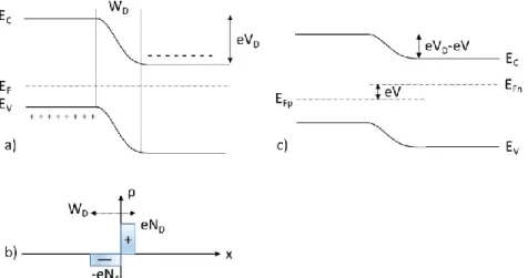
When both types of extrinsic semiconductors (n and p types) are juxtaposed, a pn junction is formed. In the contact region, electrons diffuse from the n region to the p region, and, conversely, hops from the p region to the n one. The result is the generation of a zone depleted of free carriers, called depletion region, as shown in Figure 2-1a. The only charges in the depletion region are ionized acceptors and donors, forming then a space charge region with the ionized donors in the n-side and ionized acceptors on the p-side, shown in Figure 2-1b. Contrary to the situation in the isolated material, dopants in the depletion region of a junction are fully ionized independent of the dopant activation energy. In the space charge region there is now a potential barrier which free carriers will have to overcome to reach the opposite doped neutral zone. This barrier is called Diffusion Voltage, or VD, and it is obtained by
𝑉
𝐷=
𝑘𝑇𝑒
∗ 𝑙𝑛
𝑁𝐷𝑁𝐴𝑛𝑖𝑛𝑡2 Eq. 2.1
where nint is the intrinsic carrier concentration and ND and NA are the
donor and acceptor concentrations, respectively. In practice, with doping levels in the 1018 cm-3, the diffusion voltage is close to the material band gap (divided
by e). The width of the depletion region can also be calculated considering ε, the dielectric permittivity of the semiconductor, and V, the bias voltage, by Equation 2.2.2
𝑊
𝐷= √
2𝜀(𝑉𝐷−𝑉) 𝑒∗ (
𝑁𝐷+𝑁𝐴
𝑁𝐷𝑁𝐴
)
Eq 2.2It is important to observe that this width reduces with the doping level. Under a positive bias the total energy difference between the n and p side is reduced, as shown in Figure 2-1c, and the LED will correctly function if the bias
is large enough to compensate VD, dropping the potential barrier up to a point
where electrons and holes can diffuse to their opposite sides limited only by the series resistance of the neutral regions.3,4
Figure 2-1: PN junctions at equilibrium. a) Without bias; b) Space charge region; c) Under bias.
Once a charge carrier diffuses to the neutral region of its opposite side, it can recombine with the opposite sign carrier. This is the electron-hole recombination, and it is the main light generation mechanism in homojunctions. This recombination can be radiative, i.e. emitting a photon, or non-radiative, emitting phonons instead.
2.1.1. Radiative and non-radiative recombination
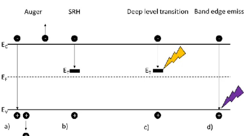
Radiative emission occurs when an electron-hole pair recombines and emits a photon of energy equal to the bandgap energy of the semiconductor used in the homojunction. It is practically impossible, however, to rule out non-radiative recombinations, so one needs to understand their causes and origins in order to minimize their presence while maximizing radiative recombinations.
When non-radiative recombination occurs, the energy of the electron is converted to a vibration of the lattice, i.e. phonons, instead of a photon. There are
several reasons for it to occur, the main being the presence of defects in the crystal structure such as dislocations, interstitials and vacancies. These defects may introduce deep levels, or traps, in the forbidden gap of the semiconductor, and radiative recombination will become unlikely – these traps are then referred to as luminescence killers, and this process is known as Shockley-Read-Hall (or SRH) recombination.2 Another type of recombination is Auger, when the energy
emitted by the e-h pair excites another charge carrier to higher levels in its band – either a conductive electron to higher levels in the conduction band, or a hole to higher levels in the valence band. It is possible that undesired radiative recombination occurs, emitting light at a different (longer) wavelength. For example, it is common for GaN that, apart from the band edge luminescence, another luminescence peak appears in the yellow range of the visible spectrum. This parasitic radiative recombination is generally known as a ‘deep level transition’, and, in the case of GaN, is thought to be due to Ga vacancies.2,5 These
recombination phenomena are represented in Figure 2-2.
Figure 2-2: Radiative and non-radiative recombinations. a) Auger; b) Shockley-Read-Hall; c) deep level transition and d) band edge emission.
The constant competition between the radiative and non-radiative recombination can be represented by the quantum efficiency ηq, which is the
fraction of excited carriers that will recombine radiatively divided by the total recombination of the structure. This parameter can be written as a function of the non-radiative and radiative lifetimes, respectively τnr and τr, as shown in
Equation 2.3:
𝜂
𝑞=
𝑅𝑟 𝑅=
𝜏𝑛𝑟
𝜏𝑛𝑟+𝜏𝑟 Eq. 2.3
where Rr and R are the radiative and total recombination rates. In order
to increase the quantum efficiency, one needs to decrease as much as possible the radiative lifetime τr.and increase the non-radiative lifetime.6
It is then essential to decrease the number of defects in the material active region – i.e the zone in which light will be generated – in order to increase ηq.
One might consider optimizing the space charge region to favor radiative recombination, in particular by introducing quantum wells and quantum dots, which will be explained in the next sections.
2.1.2. Quantum wells
Let us consider a heterostructure composed of one semiconductor with a bandgap Eg1 inserted in between two layers of a semiconductor with a bandgap
Eg2. Considering Eg2>Eg1, a potential ‘well’ will be formed. In this well, the energy
levels are quantized – thus the name ‘Quantum Well’ (QW). The role of these wells is to increase carrier confinement: when inserted in between n and p doped layers, a quantum well traps electrons and holes that will recombine radiatively.
The carrier confinement in a quantum well is two-dimensional – charge carriers are still free to move within the crystal plane of the quantum well.
Considering the hole and electron charge carrier densities p and n¸ respectively, in the electron and hole confined states, one might obtain the recombination rate R with:
𝑅 = 𝐵 ∗ 𝑛 ∗ 𝑝
Eq. 2.4where B is a proportionality constant called bimolecular recombination coefficient.2 The thickness of the quantum wells plays a critical role, with higher
3D carrier concentrations (in carriers.cm-3) and reduced carrier lifetime for
thinner quantum wells (and below the critical thickness, when plastic relaxation happens through the formation of dislocations). In the particular case of hexagonal nitride semiconductors, the thickness of the QWs also plays a role in determining the energy of the emitted light, not only through the confinement energies of holes and electrons but also through the presence of internal electric fields, which are due to the spontaneous or piezo-electric polarizations generated by misfit induced strains between the well and the barrier.2,3
If several quantum wells are juxtaposed, one obtains a multiquantum well structure (MQW). For carrier confinement in the wells, the width of the barriers must be sufficient so that the wavefunctions of adjacent quantum wells do not overlap – this results in localization of charge carriers instead of a simple tunneling process from one well to the other.
III-V semiconductor MQW structures are often used in commercially available LEDs, laser diodes and several other electronic and optoelectronic applications due to their wide range of bandgaps. In this thesis we use III-N materials, dealing only with InGaN/GaN quantum wells for blue LEDs and AlGaN/AlGaN quantum wells with different Al concentrations for UV emission.
2.1.3. The different contributions to LED efficiency
The efficiency of a light emitting diode is given in terms of its wall-plug efficiency, or WPE. This value represents physically the energy conversion efficiency from electrical to optical power. It can be calculated from Eq. 2.5
𝑊𝑃𝐸 =
ℎ𝜈𝑉
∗ 𝐸𝑄𝐸 =
ℎ𝜈𝑉
∗ 𝜂
𝑖𝑛𝑗∗ 𝐼𝑄𝐸 ∗ 𝜂
𝑒𝑥𝑡 Eq. 2.5 where hν is the energy of the photon emitted and V is the operating voltage of the device. The EQE is the acronym for external quantum efficiency, which determines the total efficiency of the light generation process in the semiconductor device. In turn, this efficiency is divided in 3 terms: internal quantum efficiency (IQE), injection efficiency (ηinj), and extraction efficiency(ηext).
The internal quantum efficiency is a direct measure of the conversion efficiency of electrons to photons – i.e. how much of the electrons injected into the active part of the structure will recombine radiatively with holes and generate light. More elegantly, it is the ratio of the number of photons emitted over the number of electron-hole pairs in the active region. In order to achieve high IQEs, it is necessary to reduce the non-radiative recombination centers such as vacancies and dislocations at the active region, so that the maximum of charge carriers entering this zone will be able to recombine and produce light.
The injection efficiency is the ratio of the electron-hole pairs in the active region by the total amount of injected carriers in the device. It relies strongly on the n and p doping levels (and especially the latter for III-Ns).
Finally, the extraction efficiency is easy to define: it is the amount of photons generated in the structure that are able to get extracted – i.e. the ratio
of the extracted photons by the generated photons in the active region. All these ratios are equally important in the WPE of LEDs: we will see that UV LEDs currently suffer from issues related to each one of them, which will be addressed in Section 2.3.2.2.
2.2. III-N materials for LED applications
The classic plot of bandgap energy by lattice parameters for (Al,Ga,In)N compound semiconductors is shown in Figure 2-3 (taking no account of the bowing parameters). It shows that higher bandgap energies can be achieved if the Al concentration in an AlGaN alloy increases.
Figure 2-3: Bandgap energy (eV) by in plane a lattice parameter (nm) for (Al,In,GaN)N systems.
However, as the aluminum concentration increases, several obstacles to the efficiency appear coming from different properties – crystallinity, polarization and acceptor binding energy. Before talking about them, a basic overview of the properties of (Al,Ga)N alloys will be presented in the next sections.
2.2.1. Wurtzite structure and spontaneous polarization
Crystals made from (Al,Ga)N materials can be arranged in 3 different structures: (hexagonal) wurtzite, (cubic) zinc blende and rock salt. However, zinc blende is metastable, rock salt requires high pressure growth procedures to be produced,7 and wurtzite is more thermodynamically stable– reasons for which
wurtzite is the structure considered in the vast majority of applications and along all this thesis.
The unit cell of the wurtzite GaN structure is represented in Figure 2-4a, with Ga and N atoms as blue and red spheres, respectively. The preferential crystal growth orientation is along the c-plane (or basal plane), and lattice parameters are c (unit height) and a (unit edge). We also note c.u the length of the III-N bond in the c –direction, which may be different from the length of the III-N bond in the three directions other than that one. In a perfect wurtzite structure (considering atoms as hard spheres), the c/a and u ratios are equal to 1.63 and 0.375, respectively. However, real crystals may be subject to a distortion and these ratios may depart from the ideal value. The result is what is shown in Figure 2-4b: there is a spontaneous polarization field generated from the deviation of the ideal lattice parameters, as well as from the dipole at the atomic level. The further the lattice parameters are from the ideal structure, the higher the spontaneous polarization field, being higher in AlN than in GaN.8 In nitride
heterostructures, an additional effect contribute to the total polarization, which arises because of the strain induced by the lattice mismatch between the substrate and the epilayers, or between lattice mismatched epilayers themselves (as in AlGaN/.GaN quantum wells for instance) .
Figure 2-4: a) Wurtzite GaN structure9; b) Spontaneous polarization by
lattice parameter u. Adapted from Wood et Jena.10
2.2.2. Lattice parameters in (Al,Ga)N and the choice of a substrate
The lattice parameters of GaN and AlN and their respective thermal expansion coefficients are shown in Table 2-1. The lattice parameters of ternary alloys, such as AlxGa(1-x)N, are given by Vegard’s law
𝑝 = 𝑥𝑝
𝐴𝑙𝑁+ (1 − 𝑥)𝑝
𝐺𝑎𝑁 Eq. 2.6 where p is the lattice parameter (either ‘a’ or ‘c’) and x is the fraction of Al in the AlxGa(1-x)N alloy.11Table 2-1. Lattice parameters of GaN and AlN and their thermal expansion coefficients11 GaN AlN a (nm) à 300K11,12 0.319 0.311 c (nm) à 300K11,12 0.519 0.498 c/a11 1.626 1.601 αa (10-6K-1)à 300K11,13 5.6 4.2 αc (10-6K-1)à 300K11,13 3.2 5.3
In order to grow a structure with good crystalline quality, one needs to choose the adequate substrate – this choice will influence the epitaxy of all
subsequent layers, together with their structural, electronic and optical quality. Table 2-2 summarizes, for the most common and available substrates, the main parameters at stake when choosing the appropriate one: their lattice parameter difference with the binaries (AlN and GaN), together with the difference in thermal coefficient of expansion (TCE) with these binaries. Often, these parameters are not sufficient, the choice being rather dictated by other factors such as the price and available wafer dimensions.
Table 2-2 : Parameters of the most used substrates for the growth of GaN et Al(Ga)N alloys.
SiC Sapphire Si (111) AlN GaN
Lattice mismatch with
epitaxied GaN (%)14 3.5 16
-17
(tensile) 2.4 0 Lattice mismatch with
epitaxied AlN (%)7,13 1 13 -19 (tensile) 0 -2.4 (tensile) αa (µK-1) à 300K14 4.7 7.5 2.6 4.2 5.6
Thermal coeff mismatch with epi-GaN (αa-GaN - α
a-sub) / αa-sub (%)
19 -25 115 33 0
Thermal coeff mismatch with epi-AlN (αa-AlN - α
a-sub) / αa-sub (%)
-10 -44 62 0 -25
Price for a 2 inches
wafer (€)14 1000 50 30 -- 1200
For example, for the epitaxy of GaN layers, and thus for blue LEDs, one might suggest the use of GaN substrates or templates. They are, indeed, the best solution if one considers only the lattice parameters and thermal expansion coefficients criteria – however, little contribution to the market has been done using these substrates, since they are technologically difficult and expensive to
fabricate. This is one of the reasons why, despite the large lattice and TCE mismatches, sapphire substrates are the most common choice for blue LEDs: all the first advancements in the field of GaN epitaxy for optoelectronics were made this substrate. It is a reasonably cheap choice, it is transparent to the visible spectra and thermally stable up to temperatures much higher than the usual nitride epitaxial temperature.14–16
However, the lattice mismatch between GaN and sapphire, shown in Section 2.2.2 should actually be a plausible reason to not choose this substrate for the epitaxy of GaN. The excessive defects generated from this mismatch in the form of high dislocation densities (possibly reaching values higher than 1010cm-2) should hinder the radiative recombination rate and, thus, the internal
quantum efficiency (IQE). Nonetheless, InGaN-QW based LEDs grown on sapphire substrates can be found with IQEs close to 100%. This is due to an effect assumed to be related to the localization of carriers in potential fluctuations within the wells (presumably caused by alloy fluctuations in the InGaN alloys) restraining the charge carriers’ degrees of freedom and avoiding non-radiative recombination in the quantum well.16–18 Note that the TCE difference between
the nitrides and sapphire leads to compressive strain in the epilayers, hence avoiding layer cracking. Instead, the use of silicon based substrates leads to tensile strained layers upon cooling from the growth temperature: in this case complex strain engineering epitaxial processes have to be implemented to avoid cracking.
For AlGaN based UV QW LEDs, there is presumably no help from localization of the charge carriers in their (Al)GaN quantum wells. In other
words, the lattice mismatch is a more concerning issue when growing high Al content AlGaN epilayers. So one could think of actually using AlN substrates found in the market, which theoretically should present the smallest lattice mismatch and are of excellent structural quality, with dislocation densities less than 104/cm². However, they are often prone to UV absorption because of the
presence of defect associated levels in the gap. In addition, they can be very expensive in comparison with the other commercially available substrates. As already pointed out in the GaN case, Si substrates have significant thermal expansion coefficient mismatch with AlN, generating internal tension and cracks in the wafer while cooling it after growth. SiC substrates could be a candidate, but their prices are not that attractive ruling them out for a commercial application. Accordingly, up to now sapphire is the substrate chosen by most of the industrial or academic groups working in the field of UV-LEDs. As said before, sapphire is thermally stable at the usual Al rich AlGaN epitaxial temperatures. Moreover Al2O3 is transparent in most of the UV domain, thus
allowing backside emission to be considered. The visible or UV emitting heterostructures used during this work were all grown onto sapphire substrates.
2.2.3. Piezoelectric field in nitride heterostructures
The lattice constant mismatches between (Al,Ga)N and their substrates are accommodated in the form of strain and misfit dislocations. In the case of GaN / AlGaN heterostructures, the lattice mismatch is moderate (around 2% between GaN and AlN) and in any case smaller than between GaN and InN (10%). Hence, in most cases, and this is compulsory for the epitaxial stack involved in the emissive heterostructures, layers are grown pseudomorphically,
i.e. without plastic relaxation. Only for thick layers, when the elastic energy exceeds a certain level corresponding to the formation of defects, plastic relaxation occurs and misfit dislocations are created. Even in that case, some strain may remain in the layers, because of uncomplete plastic relaxation.
This strain induces an additional departure from the ideal c/a ratio and thus an additional electric field, called piezoelectric field, which will add up or subtract to the spontaneous field. Eq. 2.7 gives the piezoelectric polarization on the c-axis in strained layers grown along this same axis19
𝑃
𝑝𝑧= 2 (𝑒
31−
𝑐13𝑐33
𝑒
33) 𝜖
1Eq. 2.7
where ϵ1 is the strain tensor, c13 and c33 are the elastic constants and e15,
e31 and e33 are the piezoelectric coefficients, whose values are shown at Table 2-3.
From these coefficients, valuable insight on the piezoelectric field generated by the growth (Al, Ga, In)N layers can be extracted.
Table 2-3 : Calculated piezoelectric coefficients of (Al,Ga,In)N.7,20,21
e15 (C/m2) e31 (C/m2) e33 (C/m2)
AlN -0.48 -0.6 1.46
GaN -0.3 -0.49 0.73
InN -- -0.57 0.97
The larger piezoelectric constants in AlN in comparison to GaN and InN suggest that the higher the Al content in AlGaN alloys, the stronger the piezoelectric polarization. In addition, AlN under stress should produce a higher piezoelectric polarization than GaN under stress. These assumptions are backed up by results in the literature such as those shown in Figure 2-5 in terms of the Al content in AlxGa1-xN/GaN heterojunctions grown on GaN and (Al,Ga)N
structures. The electric field discontinuity is strongly enhanced in active regions with higher concentrations of Al. Furthermore, when grown on GaN structures, the stress on the AlxGa1-xN layers of the heterojunction is higher than that of the
GaN layers – which is why the electric field discontinuity is higher.22
Indeed, this discontinuity leads to corresponding interface charges and electric fields given by
𝜌
𝑝𝑖𝑒𝑧𝑜= −∇𝑃⃗
Eq. 2.8 and𝐸⃗ = −
𝜖𝜖10
𝑃⃗
Eq. 2.9
reaching very high values such as 9MV/cm as the Al content reaches 100%, distorting the band diagram. For instance, the quantum wells are modified from a square profile to a tilted one. This effect is known as the Quantum-Confined-Stark-Effect, which causes a red shift in the wavelength of emission. In addition, the electric fields separate the electron and hole wavefunctions to opposite sides of the quantum well, decreasing their recombination efficiency and thus the internal quantum efficiency.23,24 This effect is quite common in wurtzite c-plane
structures, and is even more drastic for high Al content AlGaN structures.
Figure 2-5: Electric field discontinuity by Al content in AlGaN/GaN heterojunction active region. Adapted from Matta et al.22
2.2.4. Band structure and symmetry of the valence band
The electronic band structures of GaN and AlN are shown in Figure 2-6a and b, respectively. Both GaN and AlN are direct bandgap semiconductors at the Γ point, which means that the radiative recombination is a first order transition with no phonon involved, with a short radiative lifetime which in principle can lead to a large quantum efficiency of devices made from these materials.25,26
Figure 2-6: Electronic band structures of a)GaN and b)AlN.25,26
The valence bands in (Al,Ga)N are split in three subband levels due to the hexagonal symmetry of the structure (also called crystal-field splitting, or Δcr)
and the spin-orbit interaction. Figure 2-7 shows the band splitting and the respective points, while in red are the excitons generated by these new subband levels, indicating also the direction of the polarization of the light emitted (parallel or orthogonal to the c-axis). The bandgap value of ternary alloys such as AlGaN is given by
𝐸
𝑔𝐴𝑙𝑥𝐺𝑎1−𝑥𝑁= 𝑥𝐸
𝑔𝐴𝑙𝑁
+ [(1 − 𝑥)𝐸
𝑔𝐺𝑎𝑁] − [𝑥(1 − 𝑥) ∗ 𝑏]
Eq. 2.10where ‘x’ is the Al concentration, ‘Eg’ is the bandgap, and ‘b’ is known as
bowing parameter, which is around 1 eV for AlGaN.27
The crystal field splitting changes with the concentration of Al: it is slightly positive for GaN (~10meV), while strongly negative for AlN (~-220meV). The Γ
point then changes from Γ9 in GaN to Γ7 in AlN, so a gradual change in symmetry
might be expected as one increases the Al content in AlGaN alloys. With the change in symmetry, the emitted light changes its polarization from perpendicular (to c axis) to parallel. An extraction efficiency issue in deep UV LEDs can come out from this – problem that will be covered in Section 2.3.2.20.
Figure 2-7: Valence band splitting of a) GaN and b) AlN. The possible excitons related to holes coming from these subband levels are marked in red.26,28
2.3. UV light sources
The growing need for potable water for a population expanding such as ours, especially in countries developing under high growth rates, relates to the demand for drinkable water, hygiene and safety concerns over food and healthcare. The days of purifying water using chemical treatments are closer to being past due to the use of ultraviolet light sources to kill the bacteria: high energy UV light causes the dimerization of the bacteria and other pathogens’ DNA by forming covalent bonds between adjacent bases, preventing the replication of the nucleic coding and killing the organism.29 The proven
germicidal effect of UV light (with a germicidal effect peak at 264nm) motivated the extensive development of UV disinfection equipment.
A considerable share of this UV sterilization market is taken by UV lamps. Since the first full scale UV lamp disinfection system in 1910 to purify the waters
of the river Durance, in southern France, the market of UV lamps has considerably increased.30 These lamps are capable of providing high output power
UV light, being the most used UV light sources nowadays – we will briefly overview the subject in the next section.
2.3.1. Present day UV lamps for sterilization
Almost all of the commercial UV lamps used for sterilization generate UV radiation through a gas discharge.31 The most common lamps are mercury-based,
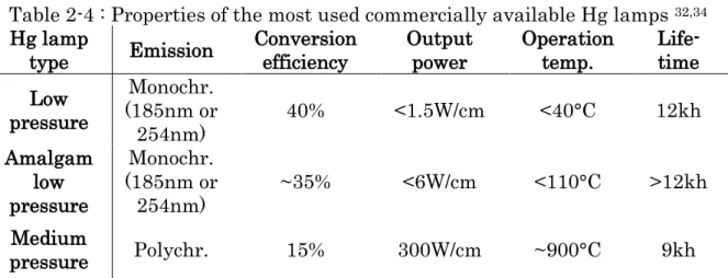
and they are usually divided in three types: low pressure (LP), amalgam low pressure (ALP) and medium pressure (MP).
The operating characteristics of each of these types are shown at Table 2-4. While low pressure lamps can achieve considerably high conversion efficiencies, their output powers, in W per unit length of the discharge arc, are low in comparison to amalgam low pressure and medium pressure lamps. The latter are those who can achieve the highest output powers, but at the cost of conversion efficiency and with a high operation temperature, which decreases the final lifetime of the system. 32,33
Table 2-4 : Properties of the most used commercially available Hg lamps 32,34
Hg lamp type Emission Conversion efficiency Output power Operation temp. Life- time Low pressure Monochr. (185nm or 254nm) 40% <1.5W/cm <40°C 12kh Amalgam low pressure Monochr. (185nm or 254nm) ~35% <6W/cm <110°C >12kh Medium pressure Polychr. 15% 300W/cm ~900°C 9kh
Although ALP and MP lamps can emit light with high efficiency and high optical powers respectively, still they present numerous drawbacks. First of all,
these systems are significantly bulky. In addition, the high optical powers achieved by these lamps come with the cost of significant increases in voltage, and thus in the end the wall-plug efficiency, which counts on the operating voltage of the device, will be reduced to values around 15 to 30% and generate considerable heat. These systems also possess slower on/off switching times with short lifetimes.35,36
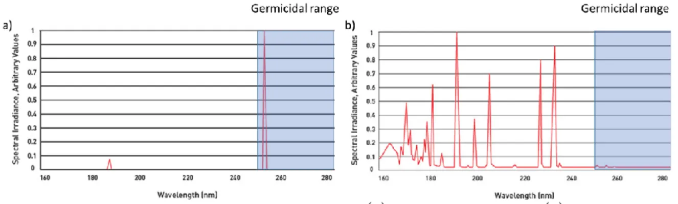
And even if the lifetimes and operating voltages of mercury lamps were to be optimized, two additional facts interfere with their application. LP and ALP lamps emit at fixed wavelengths (185 or 254nm), while MP lamps exhibit a polychromatic broad emission over several wavelengths at the same time, as exhibited in Figure 2-8. Thus, these lamps become useless for applications that demand monochromatic light different from those fixed wavelengths.
Figure 2-8. UV-C light emission peaks of (a) low pressure and (b) medium pressure Hg lamps. Adapted from ‘Aquafine’ website.37
Last but not least, the high toxicity of mercury to the human body and to nature lists these lamps as environmentally unfriendly, especially after the Minamata Convention that decided on the worldwide gradual decrease of the usage of Hg. All these reasons motivate the search for alternative UV light sources. UV LEDs, in turn, are promising and clean light sources that potentially
can overcome Hg lamps to produce light in a much more efficient and cleaner way.
2.3.2. UV LEDs
UV LEDs generate light through semiconductor devices – a cleaner and less toxic process than using mercury. Additionally, the liberty of tuning the emission wavelength to a targeted value just by adjusting the thicknesses and composition of each semiconductor layer widens the array of potential applications to these devices, such as those shown in Figure 2-9 as a function of the UV wavelength. The UV spectrum is divided in 3 sectors: UV-A (from 360 to 320nm), UV-B (from 320 to 280nm) and UV-C (shorter than 280nm).38
Figure 2-9. Potential applications for UV sources.38
More applications to UV-LEDs are already at use. UV printing, painting, tanning and curing are currently the most used applications in the UV-A spectrum, corresponding to 50% of the global UV LED market in 2017.In this wavelength range, the competition brought by UV LEDs to the conventional Hg lamps is much stronger at present. Indeed, UV-A LEDs are able to reach external quantum efficiencies of around 60% at 405nm and 50% at 385nm. 32% of the UV
LED market in 2017 corresponded to UV-B applications, mostly for phototherapy applications in the domain of skin diseases such as psoriasis and vitiligo.39,40
However, it is for sterilization that the potential application is more relevant. The already mentioned control of the wavelength is even more interesting, as UV-LEDs can be tuned to operate at the exact germicidal peak wavelength (264nm) hence increasing the efficiency of the sterilization. UV LEDs, much more compact than Hg lamps, could potentially overcome them, in as much as they would offer higher wall-plug efficiency and longer lifetime. Because of the many possibilities in terms of applications, the global UV LED market is expected to reach a value of more than 1.3 billion US dollars by the year 2024. The potential take-over of the UV-C market by UV LEDs is represented by the growth of their respective markets: the compound annual growth rate of UV LEDs is expected to reach 25% against the 14% CAGR of Hg UV lamps.30,39.
2.3.2.1. Current state of UV-B and UV-C LEDs
The actual state of the art of UV LEDs in terms of optical power is still behind Hg UV lamps. While the latter can achieve higher output powers, UV LEDs best performance at the germicidal peak wavelengths (~260nm) is close to 30mW, as shown in Table 2-5 along with the best performances of industrial UV-LEDs at several wavelengths.41 Academically, the output power at 100mA and
maximum EQE obtained by a 266nm UV LED are around 8mW and 3.5%, respectively.42 Because of these poorer characteristics compared to UV lamps,
Table 2-5 : Current state of the art on optical powers of UV-B and C LEDs.41
Companies Single chip package best performance LG Innotek (Japan) • 305nm: 10mW@100mA
• 278nm: 100mW@350mA
Dowa (Japan) • 310nm: 35mW@350mA
• 280nm: 25mW@350mA Seoul Viosys/SETi
(KOR/US) • 275nm: 50mW@600mA
Crystal IS/Asahi
Kasei (US/Japan) • 250-280nm: 30-40mW@500mA Nikkiso (Japan) • 280nm: 50mW@350mA
QD Jason (Canada) • 280nm: 5-20mW@350mA
In addition, higher participation of UV-C LEDs in the global UV-LED market suffers from the high prices per Watt of these devices, as shown in Figure 2-10. While UV-A LEDs can be found for 40 to 90 cents per Watt, UV-C LEDs remain at costly prices such as $2 per milli-Watt. Even so, the clear advantages of UV-C LEDs over UV lamps is so attractive that several major players in the LED industry, such as those listed in Table 2-5, are already on the market or ready to fully jump in.41
The specific reasons behind this overpricing in deep UV LEDs are many, all related to a reduction in the LED efficiency as the Al content of AlGaN alloys increases.
2.3.2.2. Obstacles for the External quantum efficiency of UV LEDs
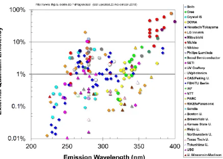
As shown by Figure 2-11, there is a steep drop in the EQE of UV LEDs when decreasing the wavelength of emission. As the wavelength decreases, the UV LED suffers from epitaxial, polarization and electrical issues. These obstacles for obtaining efficient UV LEDs will be covered in the next three sections, respectively.
Figure 2-11. External quantum efficiency by the wavelength of emission.43
Internal quantum efficiency issue
The IQE depends on the radiative recombination rate in a device. This definition suggests that internal quantum efficient LEDs should have a high radiative recombination rate compared to non-radiative. From Section 2.1.1 we learned that defects, such as dislocations and point defects, act as non-radiative recombination centers, so an LED with high IQE must have a high quality active region, with as few non-radiative defects as possible. As shown in Figure
2-12,non-radiative defects such as dislocations strongly influence the (simulated) IQE, as soon as their density exceeds 108cm-².7,44 More quantitatively, the typical
distance between defects should be longer than the lateral carrier diffusion length in the wells. If present, carrier localization will then help reaching this criterion, as it is the case with InGaN/GaN quantum wells used for blue LEDs which explain the high performance of these LEDs even in structures containing high dislocation density values such as 5x108cm-2.45
The largest problem in our case is due to these dislocations. The large lattice mismatch between sapphire and (Al,Ga)N generates dislocations that will thread along the epitaxial stack (thus the name threading dislocations, or TDs), passing through the quantum well and killing part of the luminescence.45 Carrier
localization has been reported in AlxGa1-xN quantum wells through compositional
modulation induced by macrosteps artificially introduced in the AlN buffer, but not sufficiently to compensate for the high dislocation density.42,46 Furthermore,
Al has a low mobility at the growth surface due to the large bond strength between Al and N, and during epitaxy small islands will be formed, generating additional TDs.47 For these reasons, the TD density can reach values as high as
1011cm-2 in high Al content AlGaN.7
Since AlN substrates are limited by size and price, as seen in Section 2.2.2, several trials were performed to diminish the generated dislocation density in the AlN buffer on different substrates. For instance, in the case of Si substrates, the use of ex-situ low temperature (LT) AlN templates could be an alternative to increase the crystalline quality of the subsequent AlGaN layers. In this case, the AlN template was deposited using Pulse Laser Deposition (PLD) with a low
deposition temperature (650°C) and then transferred to the MOCVD to grow the AlN buffer layer and the full LED structure. The use of these templates have increased by 39% the light emission of the LEDs.48
On sapphire substrates, AlN buffer layers were recently grown using migration enhanced epitaxy (MEE) on MBE, which has been shown to decrease the threading dislocation density to 2x109cm-2.49 Matta et al. reported the use of
low temperature buffer layers reducing the edge threading dislocation density by 75%, proving the high interest of these layers for the growth of high Al content AlGaN alloys on sapphire.50 These buffer layers underwent a thermal annealing
of 940°C – and this thermal annealing has also been thoroughly studied in the literature. For instance, strong reductions in defect density (up to 75%) were shown after a high temperature annealing (1650°C) of AlN thin films grown on sapphire substrates by MBE.51 In MOCVD, annealing treatments at 1700°C were
reported being able to achieve TD densities of 5x108 cm-2.52 More recently, it was
shown that this high temperature annealing removes almost all the stresses related to lattice mismatch, remaining with only the compressive strain during the cooldown due to the difference in the thermal expansion coefficients of AlN and sapphire.53
Alternatively, interesting results have been obtained by annealing MOCVD AlN layers that were grown on AlN previously sputtered on sapphire. With the optimal annealing performances obtained between 1600°C and 1700°C, threading dislocation densities until the low 108 cm-2 could be obtained.54–56 The
technique was also employed by Susilo et al. to develop an AlGaN UV-C LED (λ=268nm) on top of a MOCVD AlN HT annealed buffer layer on a physical vapor