HAL Id: hal-00436701
https://hal.archives-ouvertes.fr/hal-00436701
Submitted on 14 Apr 2021
HAL is a multi-disciplinary open access
archive for the deposit and dissemination of
sci-entific research documents, whether they are
pub-lished or not. The documents may come from
teaching and research institutions in France or
abroad, or from public or private research centers.
L’archive ouverte pluridisciplinaire HAL, est
destinée au dépôt et à la diffusion de documents
scientifiques de niveau recherche, publiés ou non,
émanant des établissements d’enseignement et de
recherche français ou étrangers, des laboratoires
publics ou privés.
Large electromechanical coupling factor film bulk
acoustic resonator with X-cut LiNbO3 layer transfer
M. Pijolat, S. Loubriat, S. Queste, D. Mercier, A. Reinhardt, E. Defaÿ, C.
Deguet, L. Clavelier, H. Moriceau, M. Aïd, et al.
To cite this version:
M. Pijolat, S. Loubriat, S. Queste, D. Mercier, A. Reinhardt, et al.. Large electromechanical
cou-pling factor film bulk acoustic resonator with X-cut LiNbO3 layer transfer. Applied Physics Letters,
American Institute of Physics, 2009, 95, pp.182106. �10.1063/1.3258496�. �hal-00436701�
Large electromechanical coupling factor film bulk acoustic resonator
with X-cut LiNbO
3layer transfer
M. Pijolat,1,a兲S. Loubriat,1S. Queste,2D. Mercier,1A. Reinhardt,1E. Defaÿ,1C. Deguet,1 L. Clavelier,1H. Moriceau,1M. Aïd,1and S. Ballandras2
1
CEA, LETI, MINATEC, Grenoble, Isere 38000, France
2
FEMTO-ST UMR CNRS-UFC-ENSMM-UTBM 6174, Besancon 25030, France
共Received 8 July 2009; accepted 14 October 2009; published online 5 November 2009兲
As layer transfer techniques have been notably improved in the past years, lithium niobate共LiNbO3兲
appears as a candidate for the next generation of ultrawide band radio frequency 共rf兲 filters. Depending on the crystalline orientation, LiNbO3 can achieve electromechanical coupling factors
Kt2more than six times larger than those of sputtered aluminum nitride films. In this letter, a process
based on direct bonding, grinding, polishing, and deep reactive ion etching is proposed to fabricate a single crystal LiNbO3film bulk acoustic resonator. From the fabricated test vehicles, Kt2of 43%
is measured confirming the values predicted by theoretical computations. © 2009 American
Institute of Physics.关doi:10.1063/1.3258496兴
rf passband filters are required in telecommunication systems to select the working band of the rf signal. In that purpose, piezoelectric materials are used to develop passive solutions such as surface acoustic wave共SAW兲 filters or bulk acoustic wave 共BAW兲 filters which for years have satisfied mobile phone standards. Among theses acoustic-wave-based filters, one operating mode is particularly used due to its design simplicity and adaptability, based on impedance ele-ment association as for the so-called ladder structure for in-stance. In that specific case, two kinds of resonators are con-nected; one having its parallel resonance corresponding to the series resonance of the other one. The bandwidth of the filter is proportional to the frequency spacing between series and parallel resonances, respectively, fsand fpof one of these resonators. For a BAW configuration, where ac polarization is applied between the two faces of the layer, this spacing is linked to the electromechanical coupling factor Kt2by
Kt2= 2 fs fp 1 tan
冉
2 fs fp冊
. 共1兲For the next generations of ultrawide band rf filters for which relative bandwidth in excess of 10% and drastic loss require-ments共less than 3 dB within the passband兲 are mandatory, no immediate solutions emerge. Indeed SAW filters are still lim-ited by their power handling capability.1 For BAW devices, the only efficient filters are already commercialized and based on sputtered aluminum nitride. In spite of suitable quality factors for telecom applications, AlN is not suited for ultrawide band as its intrinsic coupling factor Kt2is limited to 7.5%.1,2An alternative to AlN would be ZnO based resona-tors; however they do not exhibit higher values for either Kt2 or Q factor.2To overcome the coupling factor problem, sput-tered or sol gel depositions of lead-zirconate-titanate and lead-manganese-niobium-titanate have been investigated de-spite the major issue of limited Q factors due to relaxation of ferroelastic domain walls at the gigahertz range.2,3
The solution consisting in the use of single crystal ma-terials such as LiTaO3or LiNbO3for reaching larger Kt2and
Q factors is particularly regarded here. These materials are extensively used for the manufacture of SAW filters. Both materials exhibit large electromechanical coupling coeffi-cients and excellent quality factors, clearly larger than those of sputtered piezoelectric films for BAW resonators as their frequency/quality factor products largely overcome 1013
whereas sputtered film-based solution rarely reach this value. Moreover, in BAW configuration these two materials can exhibit electromechanical coupling factors up to 45% 共for LiNbO3兲, i.e., more than twice those of SAW devices.
Since 1970s, layer transfer appears to be a promising method to obtain pure single crystal thin films.4 Grinding polishing5,6 and the more advanced technique of ionic implantation7–9have proven the advantage of the extra free-dom for the choice of crystalline orientations and thus the choice for acoustic waves, coupling factors or temperature coefficient of frequency.
Comparing the single crystal acoustic properties to those of sputtered thin films, one can wonder that the use of thinned single crystal layers in place of deposited AlN films in rf filters should yield notable increase in coupling and quality factors, as single materials should noticeably be less affected by structural defects due to the film fabrication pro-cess共grains, columns, cracks, and orientation defects兲 which generates physical dispersion and hence acoustic losses. These advantages more than compensate the difficulties of the single crystal thin film transfer process.
The aim of this letter is to prove the feasibility of single crystal lithium niobate film bulk acoustic resonator共FBAR兲. Although standard FBAR applications need frequencies above the gigahertz, we will in this letter discuss direct wafer bonding and grinding-polishing of x-cut LiNbO3 down to 6.6 m, corresponding to a resonant frequency near 250 MHz. A final single crystal LiNbO3 FBAR obtained with
very large electromechanical coupling factor Kt2.
In order to validate such a process, two different wafers are involved. A 100 mm wafer of X-cut lithium niobate, further considered as donor or “D” is used for the two shear waves electromechanically coupled in BAW configuration. A
a兲Electronic mail: mathieu.pijolat@cea.fr.
APPLIED PHYSICS LETTERS 95, 182106共2009兲
second double-side polished Si wafer is used, further consid-ered as handling or “H” wafer.
After substrate cleaning, a metallic electrode AlCu 共100 nm兲 layer and a silicon oxide layer are deposited on the donor wafer. Another layer of SiO2共200 nm兲 is also depos-ited onto the handling wafer and then, the surfaces are cleaned and prepared for room-temperature hydrophilic bonding. On both H and D wafers, surface roughness is controlled to be less than 5 Å rms as measured by AFM 1 ⫻ 1 m2. Then a direct bonding of H and D wafers is
performed at the two silicon dioxide surfaces. Grinding followed by polishing of the rear face of lithium niobate 共D wafer兲 is achieved with a careful control of process pa-rameters. An aluminum共100 nm兲 top electrode is finally de-posited and two port resonator patterns are obtained via an ion beam milling technique.
At this step the device is a high overtone bulk acoustic resonator 共HBAR兲 and has been electrically characterized with a vector network analyzer with a short-open-load-thru calibration procedure. In HBAR, although the thinned piezo-electric layer acts as transducer, the acoustic wave mainly propagates into the substrate. The resulting measurement is a set of peaks corresponding to the high order harmonics of the thickness resonance of the substrate, modulated by the be-havior of the thinned piezoelectrically active layer. This modulation corresponds to the response of an equivalent thinned layer transducer on a semi-infinite substrate. Trans-duction efficiency is evaluated across the electromechanical coupling factor Kt2 of the thinned piezoelectric layer and is obtained from Fig.1共a兲with Eq.共1兲. In this HBAR, Kt2of the thinned piezoelectric film can be evaluated considering the modulation of the LiNbO3 X-cut resonator multimode re-sponse. Along that approach, Kt2is found to reach a top value of 45%关Fig.1共a兲兴, which is more than six times larger than AlN theoretical value of 7%. For acoustic wide band filtering solutions, submicron thick monolithic layers of lithium nio-bate would be required, possibly obtained by the Smart Cut™ technology to solve both homogeneity and reduced thickness matters.10
A final deep reactive ion etching step using the Bosch process enables the etching of the rear face of Si H wafer共550 m兲 with the SiO2as an etch-stop layer. Hence
the remaining resonator stack is composed as follows: Al 共100 nm兲/X-cut LiNbO3共6.6 m兲 / AlCu共100 nm兲 /
SiO2共400 nm兲. This FBAR is tested along the same
proce-dure as for the previous HBAR. Figure 1共b兲 shows the first two harmonics and this time a Kt2 of 43% is directly
ex-tracted from these measurements via Eq.共1兲.
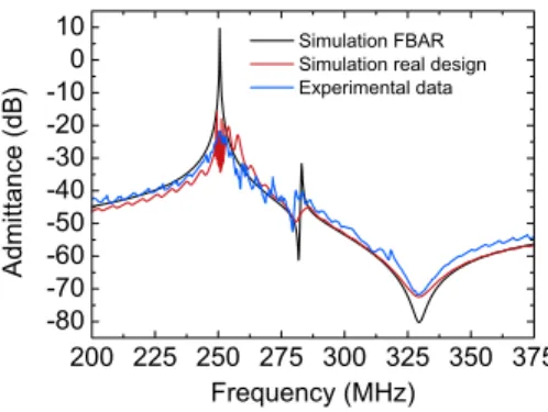
For further understanding of this resonator, we use simu-lations based on the scattering matrix method.11This method includes a Fahmy/Adler formulation,12 which describes vi-brations of multilayered structures as the linear superposition of plane waves propagating in each layer. Electromechanical fields are then calculated from the applied boundary condi-tions共stress-free surfaces, continuity at the interface between two materials, and electrical excitation兲, which allows to de-termine the surface electrical charge density at the interface between the excitation electrode and the piezoelectric mate-rial and from this the electrical admittance or impedance. Figure2shows the corroboration of the large value obtained experimentally 共in blue兲 and from simulations based on the scattering matrix method共in black兲. Similarly one can calcu-late from the material constants the theoretical value of 45%, close to the experimental value of 43%.
Beyond the large electromechanical coupling factor measured, the consistency between the HBAR extraction and FBAR measurements is of great interest. A rather good ap-proximation of this value is easily obtained with HBAR.
However, it is worth noting that the tested resonators did exhibit quite poor quality factors共in the vicinity of 64兲. The origin of this disappointing result is due to the thickness homogeneity degradation while performing the grinding op-eration. From surface profiler measurements, we observed a linear thickness difference of 100 nm across the 150 m width of the active area of the tested resonators. As fre-quency is inversely proportional to the thickness and quality factor is extracted from the full width at half maximum of conductance peaks, even for a nonlossy material a 100 nm shift in thickness is the limiting effect concerning the quality factor.
Indeed, we can write for the first mode with the approxi-mation
FWHM⬇ fr共e兲 − fr共e + ⌬e兲 =
v 2e− v 2 ·共e + ⌬e兲 = 2v · ⌬e 4e ·共e + ⌬e兲, 共2兲
FIG. 1.共Color online兲 共a兲 High order harmonics of the HBAR modulated by the first two harmonics of the thinned LiNbO3layer. From the modulation of the thin piezoelectric layer fs and fp are the extracted series and parallel resonances of this thin layer.共b兲 Fundamental and third harmonics of the pure shear mode of the self-supported thinned X-cut LiNbO3plate. A Kt2 close to 45% is measured. Insets in 共a兲 and 共b兲 are schematic views of HBAR and FBAR LiNbO3, respectively.
FIG. 2. 共Color online兲 Comparison of the first resonance of a FBAR re-sponse simulated considering a homogeneous thickness on the LiNbO3, as-suming an inhomogeneous thickness of the LiNbO3plate simulated by 20 resonators connected in parallel , and compared to the experimental admit-tance of the resonator.
Q= fr FWHM= v 2 · e. 4e ·共e + ⌬e兲 2v · ⌬e = e+ ⌬e ⌬e = 1 + e ⌬e, 共3兲 where fr共e + ⌬e兲 and fr共e兲 are the resonant frequencies of a
resonator with the maximum thickness e + ⌬e and minimum thickness e, respectively. Q is the quality factor, and v the velocity of the acoustic wave considered. Numerically, for the 6.6 m thickness e of our FBAR and with ⌬e = 100 nm, Q is limited to 67. The same calculation based on an optical interferometer measurement of surface roughness of 0.6 nm rms—i.e., ⌬e = 1.2 nm—would lead to a maxi-mum Q of 5500, comforting the idea that the limiting effect is the inhomogeneous thickness.
Based on the scattering matrix method, simulations are performed with 20 parallel resonators—LiNbO3 material Q
is set above 10 000—with thicknesses distributed from 6.55 to 6.65 m, providing a good approximation of the actual FBAR 共in red兲. The result is in good agreement with the previous explanation as shown in Fig.2. A broader peak on the resonator conductance is observed leading to a poorer quality factor, as experimentally observed. Matching with experimental data is performed reinforcing the hypothesis of linear thickness increase. Two other phenomena are observed in Fig. 2.
• The fast second shear wave appears between series and parallel resonance of the slow shear wave with larger Kt2 than what is experimentally observed.
• Oscillations around the resonance peak and for frequencies higher than the antiresonance peak are HBAR behavior due to the design of our two ports resonators.
Finally, we can take into account the material properties extracted from simulations to show what would be a typical acoustic wide band filter in the gigahertz range. Figure3is a comparison between a standard Global System for Mobile communications band pass filter based on solidly mounted AlN resonators and a possible ultra wide band filter based on LiNbO3FBAR. More than six times larger bandwidth is
ob-served.
In this letter, a 6.6 m single crystal X-LiNbO3FBAR
has been fabricated by wafer bonding, grinding polishing and deep reactive ion etching. A Kt2 value as high as 43% is demonstrated and compared to theoretical and simulated val-ues. However, it has been shown that controlling accurately the thinned layer thickness reveals to be a key-parameter for reaching high Q factor resonances. Larger quality factors as well as thinner layers might be achieved by improvement of
the process or more advanced techniques such as Smart Cut™ in order to obtain sub micron single crystal piezoelec-tric layers10 and hence the feasibility of ultrawide band rf filters.
This work has been performed with the help of the “Plateforme technologique amont” de Grenoble, with the fi-nancial support of the “Nanosciences aux limites de la Nanoélectronique” Foundation.
1R. Aigner, Proceedings of the International Ultrasonic Symposium, 582 共IEEE, Beijing, 2008兲.
2P. Muralt, J. Antifakos, M. Cantoni, R. Lanz, and F. Martin, Proceedings
of the International Ultrasonic Symposium, 315共IEEE, Rotterdam,2005兲. 3H. P. Lobl, M. Klee, R. Milsom, R. Dekker, C. Metzmacher, W. Brand,
and P. Lok,J. Eur. Ceram. Soc. 21, 2633共2001兲.
4H. C. Huang, J. D. Knox, Z. Turski, R. Wargo, and J. J. Hanak, Appl.
Phys. Lett. 24, 109共1974兲.
5S. H. Christiansen, R. Singh, and U. Gösele,Proc. IEEE 94, 2060共2006兲. 6Y. Osugi, T. Yoshino, K. Suzuki, and T. Hirai, Proceedings of the MTT-s
International Microwave Symposium, 873共IEEE, Honolulu,2007兲. 7B. Aspar, H. Moriceau, E. Jalaguier, C. Lagahe, A. Soubie, B. Biasse, A.
M. Papon, A. Claverie, J. Grisolia, G. Benassayag, F. Letertre, O. Rayssac, T. Barge, C. Maleville, and B. Ghyselen, J. Electron. Mater. 30, 834 共2001兲.
8K. Diest, M. J. Archer, J. A. Dionne, Y. B. Park, M. J. Czubakowski, and H. A. Atwater,Appl. Phys. Lett. 93, 092906共2008兲.
9M. Pijolat, J. S. Moulet, A. Reinhardt, E. Defaÿ, C. Deguet, D. Gachon, B. Ghyselen, M. Aïd, and S. Ballandras, Proceedings of the International
Ultrasonic Symposium, 201共IEEE, Beijing,2008兲.
10J. S. Moulet, M. Pijolat, J. Dechamp, F. Mazen, A. Tauzin, F. Rieutord, A. Reinhardt, E. Defaÿ, C. Deguet, B. Ghyselen, L. Clavelier, M. Aïd, S. Ballandras, and C. Mazuré, Proceedings of the International Electron
De-vices Meeting共IEEE, New York, 2008兲.
11A. Reinhardt, Th. Pastureaud, V. Laude, and S. Ballandras,J. Appl. Phys. 94, 6923共2003兲.
12A. H. Fahmy and E. L. Adler,Appl. Phys. Lett. 22, 495共1973兲. FIG. 3. 共Color online兲 Comparison of nonoptimized simulated pass band filters based on X-cut LiNbO3and traditional sputtered AlN. The simula-tions are performed with the scattering matrix method. The stacks of AlN and LiNbO3band pass filters are designed so as to provide center frequency close to 2 GHz.