HAL Id: tel-00779457
https://tel.archives-ouvertes.fr/tel-00779457
Submitted on 22 Jan 2013HAL is a multi-disciplinary open access archive for the deposit and dissemination of sci-entific research documents, whether they are pub-lished or not. The documents may come from teaching and research institutions in France or abroad, or from public or private research centers.
L’archive ouverte pluridisciplinaire HAL, est destinée au dépôt et à la diffusion de documents scientifiques de niveau recherche, publiés ou non, émanant des établissements d’enseignement et de recherche français ou étrangers, des laboratoires publics ou privés.
Misfit dislocation and strain relaxation at large lattice
mismatched III-V semiconductor interfaces
Y. Wang
To cite this version:
Y. Wang. Misfit dislocation and strain relaxation at large lattice mismatched III-V semiconductor interfaces. Materials Science [cond-mat.mtrl-sci]. Université de Caen, 2012. English. �tel-00779457�
UNIVERSITE DE CAEN /BASSE-NORMANDIE
U.F.R.: Sciences
ECOLE DOCTORALE: SIMEM
THESE
Présentée par
M. Yi WANG
Et soutenue le 20 juin 2012 En vue de l’obtention du
DOCTORAT de L’UNIVERISTE DE CAEN
Spécialité: Milieux denses, matériaux et composants (Arrêté du 07 août 2006)
Titre :
Dislocation et relaxation des contraintes aux interfaces
entre semiconducteurs III-V à large différence de
paramètres de maille
MEMBRES du JURY
M. Eric Tournié Professeur, Université de Montpellier II Rapporteur M. Martin Hÿtch Directeur de Recherche CNRS, CEMES, Toulouse Rapporteur M. Ludovic Desplanque Maître de conférences, Université de Lille I
M. Slawomir Kret Chercheur, Institut de Physique, Varsovie, Pologne M. Richard Rizk Directeur de Recherche CNRS, CIMAP, Caen
M. Jun Chen Maître de conférences, Université de Caen Co-dicteur de thèse M. Pierre Ruterana Directeur de Recherche CNRS, CIMAP Dicteur de thèse
Acknowledgements
Along these three years in CIMAP, I have come across a number of people who gave me support, help, and inspiration. It is impossible to mention everyone and I therefore would like to start by thanking all of you for contributing to my thesis.
However, I would like to mention my supervisor Dr. Pierre Ruterana for giving me the opportunity to carry out my PhD Research work in the scope of the ANR project MOS35 and for leading me into the field of electron microscopy and dislocations. Along these three years, he has given me guidance, support, and encouragements for my research, and helped to keep my curiosity always alert; Dr. Jun
Chen, my co-supervisor for teaching me molecular dynamics and ab initio simulations, and also for
the numerous and fruitful discussions.
Indeed, I’d like to thank Dr. Slawomir Kret for teaching me strain mapping analysis by GPA and hosting me for experiments with his Titan microscope. I have always enjoyed the visits to IFPAN and hope that we can continue such a fruitful collaboration.
Of course, I owe very much to our MOS35 project partner, the MBE growth group of IEMN Lille: Dr.
Ludovic Desplanque, Selim El Kazzi, and Dr. Xavier Wallart for providing me with samples as
well as for all the interesting discussions during and outside the project meetings.
I am highly grateful to Prof. Eric Tournié, Dr. Martin Hÿtch, for having reviewed this manuscript and allowed me to present my results in front of the PhD examination committee. Thank you also Dr.
Ludovic Desplanque, Dr. Slawomir Kret, and Dr. Richard Rizk for kindly having accepted to take
part in the committee of my examination.
My colleagues, Marie-Pierre Chauvat for teaching and helping me with sample preparation; Dr.
Bertrand Lacroix, Arantxa Vilalta-Clemente and Geeta Rani Mutta for all the good discussions in
research and life.
And all my friends in Caen for making my life colorful all along these years. My wife, Yi JIANG, and my parents, for endless love and support.
Dislocation et relaxation des contraintes aux interfaces entre
semiconducteurs III-V à large différence de paramètres de
maille
Les semiconducteurs III-V antimoniés suscitent un intérêt grandissant pour les applications en électronique rapide et pour les faibles consommations. Ces matériaux de paramètre de maille supérieur à 6.1 Å se caractérisent par des mobilités élevées et offrent une souplesse inégalée pour l’ingénierie des bandes. Ils ont une large plage de la bande d’énergies qui peut être ajustée dans une gamme de longueur d'onde du proche infrarouge (AlSb, 0.78 µm) à l'infrarouge lointain (InAsSb, 12 µm). Leurs hétérostructures peuvent présenter des alignement des bandes de type I (la bande interdite de plus faible largeur est inclue dans cellede plus grande largeur), alignement de type II (alignement en escalier), et alignement de type III (alignement continu sur l’une des bandes (conduction ou valence) répercutant l’intégralité de l’écart de largeur de bande interdite sur l’autre bande). Outre la structure de bande unique, les propriétés physiques, en particulier la mobilité des porteurs, constituent la distinction entre les antimoniures et les autres semiconducteurs III-V. GaSb est particulièrement intéressant en tant que couche de tampon pour la croissance des autres III-V composés de la famille 6.1 Å.
Toutefois, la croissance des III-V antimoniés sur des substrats disponibles dans le commerce (Si, GaAs, et GaP) posent des problèmes à cause des larges désaccords de paramètres de maille, différence des coefficients de dilatation thermique ainsi que des changements dans la structure chimique et polaire / non polaire décalage (sur substrat Si) à l'interface. En raison de ces problèmes d'incompatibilité, les tentatives pour déposer III-V antimoniés directement sur la GaAs (ou Si ou GaP) conduisent à des couches avec de fortes densités de dislocations émergeantes de l'ordre de 10-9-1010 cm-2. Ces dislocations peuvent se propager à la couche active et entraver considérablement la fiabilité des dispositifs.
En général, dans les hétéro-structures de structure cubique, deux types des dislocations d’interface: les dislocations à 90o et les dislocations à 60o, peuvent se former aux interfaces. Les dislocations à 90o sont aussi appelées ‘dislocations de Lomer’ du fait qu’elles jouent un rôle de barrière dans les plans {111} à cause de leur nature sessile. Les dislocations à 60o sont caractérisées par leur vecteur de Burgers incliné par rapport à l’interface avec un angle de 60o avec la ligne de dislocation; elles sont glissiles dans un des plans {111}. Les dislocations à 60o qui se propagent dans le volume, dislocation émergentes, sont aussi appelées ‘threading dislocations’. Récemment, il a été proposé que des conditions particulières de croissance pourraient conduire à une formation exclusive des dislocations de Lomer aux hétérointerfaces. Un tel réseau hautement périodique des dislocations de Lomer dans la croissance de GaSb sur GaAs donnerait alors des couches très relaxées (∼ 98%) avec une très faible densité de dislocations émergentes (~105 cm-2). L’objectif scientifique de ce travail a été d'abord de comprendre les problèmes de croissance associés à la différence des paramètres cristallins, le mécanisme de formation des dislocations d'interface dans les hétéro-structures semiconducteurs, et finalement cerner les condition pour obtenir une bonne qualité des couches épitaxiale de GaSb. Le manuscrit est divisé en cinq chapitres :
Chapitre 1 Semiconducteurs III-V antimoniés
Dan le premier chapitre nous donnons une introduction sur les propriétés des semiconducteurs III-V antimoniés, leur avantages et applications. Puis, nous présentons les problèmes associés à leur croissance, et un résumé de l’art sur leur croissance.
Chapitre 2 Des outils
Dans une première partie, nous avons décrit la technique de croissance (Molecular Beam Epitaxy) qui a été employées par nos collaborateurs (IEMN, Lille) pour réaliser toutes les couches que nous avons analysées dans ce travail. La deuxième partie de ce chapitre est dédiée à la description du principe de microscope électronique en transmission et la préparation des lames minces. L’état de l’art de la microscopie haute résolution avec correction l’aberration sphérique et l’aberration chromatique (Cs et Cc)
ce travail. Sont ensuite introduits deux de méthodes de traitement d’images : l'analyse de phase géométrique et le tenseur densité dislocation, pour l’analyse des contraintes et la détermination des vecteurs de Burgers des dislocations, respectivement. Finalement, nous rappelons des notion de la théorie de l’élasticité appliquée aux dislocations et leur interaction élastique; et la modélisation par dynamique moléculaire utilisant le potentiel empirique de Stillinger-Weber est au aussi introduite.
Chapitre 3 L’optimisation de la croissance de GaSb sur GaAs et GaP
Dan ce chapitre, nous avons fait une étude systématique de la relation entre les paramètres de croissance et les dislocations d’interface est présentée. Pour ce faire, nous avons d'abord réalisé des couches de GaSb sur le substrat de GaAs en utilisant de fines intercouches d'AlSb d'épaisseur variable pour étudier leur effets sur la densité de dislocation émergentes, les dislocations d’interface, et la relaxation des contraintes. Outre l'intercouche AlSb, l'influence de la reconstruction de la surface du substrat a été également étudiée. Sur substrat GaP, nous avons analysé la relaxation des contraintes, les dislocations d’interface à l’étape initiale de croissance, ainsi que l'optimisation de la croissance. Outre le rôle du traitement de surface du substrat et l’influence de la vitesse de croissance, la température de croissance sur la relaxation des contraintes d’îlôts de GaSb a été aussi étudiée. En utilisant les condition de croissances optimisées, des hétérostructures AlSb/InAs a été fabriquée sur les substrats GaAs et GaP avec une couche tampon de 600 nm de GaSb conduisant à de très bonnes propriétés de transport.
Chapitre 4 Le mécanisme de formation de la dislocation d’interface
Dans ce chapitre, nous avons procédé à une étude extensive de la croissance de GaSb sur GaAs, les paramètres étudiés ont été la reconstructions de surface du substrat, les traitement chimique et la température de croissance (460oC- 530oC). Dans les conditions de croissance utilisées, bien que la relaxation des contraintes soit maximisée à 510oC, le mode de croissance correspondant est trois dimensions (3D), et jusqu'à 40-50 monocouches, la coalescence de film n’est pas encore terminée. Nous avons alors proposé un modèle de relaxation capable de rendre compte de la formation de dislocation d’interface dans les hétéro-structures indépendamment de la différence des paramètres. En plus de
HRTEM, la microscopie électronique en transmission à balayage en mode champ sombre annulaire à grand angle (HAADF-STEM) et la simulation de dynamique moléculaire ont été appliquées pour déterminer la configuration atomique de dislocation d’interface. L’analyse de tenseur densité de dislocation a été ensuite utilisée pour quantifier le vecteur de Burgers des dislocations. Cette mesure précise confirme le mécanisme de formation des dislocations d’interface à GaSb/GaAs interface, qui est en accord avec le modèle que nous avons proposé.
Chapitre 4 Conclusions et Perspectives
Dans le dernier chapitre, nous résumons les conclusions de ce travail et proposons des suggestions pour poursuivre ce type de travail. Dans le cadre de projet MOS35, ce travail a participé à comprendre la formation des dislocations d'interface, et ouvert la voie pour croitre des couches GaSb de qualité électronique vers la fabrication de dispositifs performants.
En résume, les principaux résultats obtenus sont les suivants :
1. Nous avons démontré que le traitement de surface riche en Sb favorise la formation des dislocations de Lomer aux interfaces GaSb/GaAs, et GaSb/GaP.
2. Les couches ultrafines d'AlSb améliore la qualité des interfaces qui deviennent très planes. La combinaison du traitement de substrat riche-Sb et 4 monocouches d'AlSb a conduit à une relaxation mesurée de 100% de la contrainte dans les couches de GaSb sur GaAs et à densité de dislocations émergentes de 107 cm-2.
3. L’analyse de la relaxation des contraintes et de l’espacement des dislocations d’interface en fonction de la température et la vitesse de croissance, prédit une fenêtre optimale pour la croissance de couches de GaSb/ GaP avec une relaxation de l'ordre de 95% de la contrainte.
4. Avec ces paramètres optimisés, des hétéro-structures de AlSb/InAs à haute mobilité de 30000cm2V-1s-1
(25500 cm2V-1s-1) à température ambiante sur GaAs (GaP) ont été obtenues après une couche tampon GaSb de 600nm d’épaisseur.
5. Nous avons mis en évidence qu'un mode de croissance 2D conduit à la formation de dislocation de Lomer, tandis le mode 3D résulte en une formation systématique de paires de dislocations 60o aux interfaces.
6. La configuration atomique des dislocations a été étudiée par HAADF avec une résolution atomique et simulation de l’image. Les cœurs arsenic shuffle de dislocations Lomer se constituent la plus forte densité de dislocation d’interface en accord avec nos simulations numériques.
7. L’analyse du tenseur densité de dislocations montre que dans l'interface GaSb/GaAs, le mécanisme dominant pour la formation des dislocations d’interface est le glissement et la réaction des dislocations à 60o.
Suggestions pour poursuivre ce travail :
1. Une étude approfondie de l'effet de la reconstruction de surface sur la relaxation des contraintes et le mode de croissance est encore nécessaire.
2. Une deuxième préoccupation est la source des dislocations émergentes. Il sera important de comprendre comment la dislocation d'interface se transforme en dislocation émergente.
3. Théoriquement, deux types de dislocations de Lomer sont à l’interface: les configurations "shuffle" devraient se former dans l'interface (1-10) et les "glide" dans (110). Toutefois, dans l’observation expérimentale, à la fois, les configurations "shuffle" et "glide" ont été observées à l'interface (1-10). Il donc sera intéressant de déterminer les raisons de cet écart entre l’observation expérimentale et la modélisation.
Introduction
The misfit dislocations play a critical role in growth of high quality Sb-based III-V hetero-structures, which is of great interest for applications in the near- and far-infrared optoelectronics and ultra-high speed low-power consumption electronics. Due to the large lattice mismatch between the III-Sb and the substrate, large number of defects generate in the epitaxial layer. For instance, the threading dislocations originated in the hetero-interface could propagate to the surface (or active layer) thus damaging the devices. Given the large lattice mismatch, the misfit dislocations form rapidly during the growth. Both 90o Lomer and 60o dislocations are known to form at the interface, and the 60o dislocations are considered as the source of the threading dislocations. Recently, it was reported that one may find growth conditions to form a pure periodical Lomer dislocation network which releases all the misfit strain in the interface thereby obtaining high quality Antimonide based III-V semiconductors.
The aim of this work was to carry out an extensive TEM investigation of Sb-based III-V layer on the GaAs (or GaP) substrates and especially try to point out the relationship between the misfit dislocations types, strain relaxation, and the misfit dislocation formation mechanism.
In Chapter 1, the motivation for this research, the advantage of Sb based III-V semiconductors and the state of art of the MBE epitaxy of GaSb are presented.
The facilities as well as the theoretical tools used in this thesis are introduced in Chapter 2.
The Chapter 3 is an account of our growth optimization of highly lattice mismatched GaSb on two substrates (GaAs and GaP). The epitaxy of GaSb on GaAs substrate with 7.8% lattice mismatch, the influence of the surface treatment and AlSb interlayer thickness on the threading dislocation density, the fine structure of misfit dislocations, and the strain relaxation at the interface region was investigated. The epitaxy of GaSb on GaP substrate with 11.8% lattice mismatch, the strain relaxation and misfit dislocations at initial growth step (10 MLs GaSb) were studied versus substrate surface treatment, growth
iii rate, and growth temperature. This optimization process predicted an optimal window for the growth relaxed GaSb epitaxial layers on GaP.
Chapter 4 discusses our experimental and theoretical work to investigate the misfit dislocation formation mechanism. With typical (1x4) substrate surface reconstruction, a growth mode transition from 2D to 3D when the growth temperature increasing from 465oC to 510oC was observed. Most interestingly, a dependence of the misfit dislocation configuration was noticed. Based on the conventional 60o dislocation glide model, a misfit dislocation formation model was proposed. This model indicates that the misfit dislocation configurations are determined by the initial growth mode. Moreover, this developed 60° dislocation glide model is able to account for the formation of Lomer, 60o, and 60o dislocation pairs at binary zinc-blende hetero-interfaces for low as well as high lattice mismatch. Then with atomic resolution HAADF along with molecular dynamic simulation, the core structures of the misfit dislocations and their energetic stability were determined. In addition, dislocation density tensor analysis was applied on the identified misfit dislocations to quantify their Burgers vector. This precise method confirms the formation mechanism of the misfit dislocations which is in good agreement with misfit dislocation formation model we proposed.
Contents
Acknowledgments i
Introduction ii
Contents iv
Chapter 1 Antimony based III-V semiconductors 1
1.1 Antimony based compound semiconductor 1
1.2 Why ABCS 1
1.3 Overview of the Sb-based III-V semiconductors technology 5
1.4 Objective of this work 12
References 12
Chapter 2 Tools and facilities 16
2. 1 Molecular beam epitaxy 16
2.1.1 Introduction of the molecular beam epitaxy system 16
2.1.2 Specific growth 17
2.2 Microscopy 18
2.2.1 Principle 18
2.2.2 TEM sample preparation 23
2.3 Modes of operation and theoretical background 23
2.3.1 Diffraction 23
2.3.2 Bright, dark and weak beam images 25
2.3.3 HRTEM 27
2.3.4 Z-contrast imaging or STEM 31
2.4 Geometrical phase analysis and dislocation density tensor 34
v
2.5.1 Dislocations: edge and screw configurations 38
2.5.2 Burgers vector 39
2.5.3 The stress field of a straight dislocation 40
2.5.4 The strain energy of a dislocation 42
2.5.5 Elastic interaction between dislocation 44
2.6 The Molecular dynamics simulation 45
References 47
Chapter 3 The growth optimization of GaSb on GaAs and GaP substrates 50
3.1Threading dislocation density and strain relief in GaSb/GaAs versus substrate treatment and AlSb thickness 51
3.1.1 Introduction 51
3.1.2 Samples 52
3.1.3 Results 53
3.1.4 Discussion 62
3.2 Strain relief and growth optimization of GaSb on (001) GaP 63
3.2.1 Introduction 63
3.2.2 Samples 64
3.2.3 Surface treatment 65
3.2.4 Optimization of the growth rate and growth temperature 68
3.2.5 The threading dislocation density and strain relaxation in the GaSb buffer layer 70
3.3 The AlSb/InAs hertero-structure on the relaxed buffer layer 71
3.4 Conclusion 73
References 74
Chapter 4 The formation mechanism of misfit dislocations 76
4.2 Growth mode dependence of misfit dislocation types and misfit dislocation formation model 78
4.2.1 Samples 78
4.2.2 Misfit dislocation types versus growth mode 79
4.2.3 Misfit dislocation formation model 82
4.3 The atomic configuration of the misfit dislocations 87
4.3.1 Samples 87
4.3.2 The atomic configuration of misfit dislocation 88
4.3.3 The configuration stability of the misfit dislocation 90
4.3.4 The Burgers vector of the misfit dislocations and their formation mechanism 92
4.4 Conclusion 96
References 96
Chapter 5 General conclusions and Perspectives 99
5.1 Conclusions 99
5.2 Perspectives 100
References 104
1
Chapter 1
Antimony based III-V semiconductors
1.1 Antimony based compound semiconductor
In recent years, the narrow band gap antimony based compound semiconductors (ABCS) have been widely investigated as the first candidate materials for fabrication of the third generation infrared photon detectors and integrated circuits with ultra-high speed and ultra-low power consumption [1, 2]. Their applications shall include high-speed analog and digital systems for data processing, communication, imaging, and sensing, particularly in portable equipment such as handheld devices and satellites. The development of Sb-based transistors for use in low-noise high-frequency amplifiers, digital circuits, and mixed-signal circuits may provide the technology needed to address these rapidly expanding needs [2]. Generally, the ABCS refers to the Sb based binary, ternary and quaternary compound semiconductor materials, which consist of III-group elements (Ga, In, Al), Sb, and other V-group elements; such as GaSb, AlSb, InSb, AlGaSb, InAsSb, AlGaAsSb, InGaAsSb and so on. Among them, GaSb and AlSb together with InAs have been routinely called the “6.1 Å III-V family materials” in the literature due to their lattice constant of around 6.1 Å [3]. Like other compound semiconductors, they are of interest principally for their hetero-structures. GaSb is particularly interesting as an important template layer for device growth of other 6.1 Å lattice constant family of compounds.
1.2 Why ABCS?
As shown in Fig. 1.1, band gaps of ABCS can be adjusted in a wide range from near-infrared wavelength (AlSb, 0.78 µm) to far-infrared spectra regions (InAsSb, 12 µm). Their hetero-junctions can have straddling gaps (type-I), staggered gaps (type-II), and broken gaps (type III) [4, 5], as schematically
Figure 1. 1 Energy band gap and wavelength versus lattice constant [1].
shown in Fig. 1.2. In a Type-I hetero-junction, one material has both lower conduction band (Ec) and higher valence band (Ev) and naturally, it must have a smaller energy gap, in which electrons and holes are confined in one type of the constituent semiconductor layer with ground electron state belonging to the direct-gap Γ minimum of the conduction band. In a Type-II hetero-junction, the locations of lower Ec and higher Ev are displaced, so the electrons being collected at lower Ec and the holes being collected at
higher Ev are separated in the real space and confined in the layers of different semiconductors with the ground electron state belonging to (a) the indirect-gap (X or L) minimums of the conduction band or the direct-gap Γ minimum of the conduction band. A Type-III hetero-junction is a special case of Type-II, but the Ec of one side is lower than the Ev of the other. The conduction band thus overlaps the valence band at the interface, hence the name broken gap. Their variant groups of the band alignments lead to many interesting device structures which can be exploited using various combinations of these materials and their band alignments [6]. For instance, the InAs/AlSb quantum wells with type II band alignment for high mobility transistor applications [7, 8]; hetero-structures consisting of InAs contact layer, AlSb barriers, and InAs well for resonant tunneling diodes [9], and hetero-structures consisting of InAs contact layer, AlSb barriers, and GaSb well for resonant interband tunneling diode [10].
3
Figure 1. 2 Relative band alignments of narrow band gap III-V semiconductors in comparison with GaAs, along with the three types of band alignment. (b) Three types of semiconductor hetero-junctions organized by band alignments.
Table 1. 1 Bulk properties of narrow band gap III-V semiconductors at room temperature (RT) in comparison with GaAs.
InSb GaSb AlSb InAs GaAs
Lattice constant (Å) 6.4794 6.0959 6.1356 6.0584 5.6533
Mobility at RT (cm2V-1s-1)
Electron 8x10⁴ 500 200 3 x10⁴ 8500
Hole 1250 880 375 480 400
Effective mass Electron 0.018 mo 0.42 mo 0.12 mo 0.023 mo 0.082 mo
Hole 0.4 mo 0.4 mo 0.098 mo 0.42 mo 0.45 mo
Besides the unique band structure, the physical properties, particularly the carrier mobility, distinguish the ABCS from others III-V semiconductors. The comparison of ABCS’s bulk properties with those of GaAs at room temperature is summarized in Table 1.1, as can be seen; Sb-based III-V semiconductors have larger carrier mobility and smaller effective mass in comparison with those of GaAs. Indeed, the trend toward higher mobility with smaller band gap has made them a route to achieving higher speed at lower voltage and power dissipation for a given geometry as illustrated in Fig. 1.3.
Figure 1. 3 Plot of cut-off frequency versus dc power dissipation form [17] that compares the rf performance of scaled n-channel InSb and Si devices.
Regarding the relatively poor hole transport properties, researchers are trying to push the hole mobility to higher values via three strategies: (i) improving material quality, (ii) imposing strong confinement, and (iii) employing high levels of strain [11]. The best quality materials are largely the products of long-standing programs on antimonide growth by molecular beam epitaxy at the QinetiQ Corp. (for InSb) and at Naval Research Laboratory (for GaSb and InGaSb). Similar to Si and SiGe, when confinement and strain act on ABCS, the hole mobilities are enhanced because the degeneracy of light- and heavy- hole band is split, thereby raising the proportion of carriers in the higher mobility heavy-hole band and lowering the density of final states for scattering [12]. Using these strategies with quantum well thickness
in the range of 5-10 nm and biaxial compressive strains of 1-2%, p-channel mobility have been raised to into range of 1200-1500 cm2V-1s-1 [13, 14]. Moreover, there is potential for further increase, particularly
if one could reach higher strain (especially in GaSb where the best result to date has been a strain of only 0.8-1.2%), or could exert uniaxial strains as has been shown in SiGe [15] and explored theoretically for the antimonides in Ref. [16]. And even the present mobility levels, which are better than the best results in Si (though not Ge), could be sufficient for a future III-V CMOS technology. Another advantage of the antimonides is that, as in Si technology, the same material can serve as both n-channel and p-channel [7].
5 Table 1. 2 Lattice mismatch and linear thermal expansion of binary ABCS with different substrates at 300K.
Lattice constant (Å) Thermal expansion Coefficient (10-6 K-1) Lattice mismatch (%) Thermal expansion coefficient of substrates (10-6 K-1) GaAs Si GaP GaSb 6.0959 6.35 7.8 12.2 11.8 AlSb 6.1355 4.2 8.5 13.0 12.6 GaAs 6.03 InSb 6.4794 5.04 14.6 19.3 18.9 Si 2.616 InAs 6.0584 4.28 7.2 11.6 11.1 GaP 4.89
Figure 1. 4 Growth of GaSb on GaAs substrate yielding a high TDs density, 109-1010 cm-2 estimates form the
plan-view.
As shown in Fig. 1.3, a visual comparison of the cut-off frequency versus dc power of n-channel InSb and Si devices [17]. The InSb is better than Si in terms of both speed and power.
1.3 Overview of the Sb-based III-V semiconductor technology
As discussed above, ABCS are of great interest for applications in the near- and far-infrared optoelectronics and ultra-high speed low-power consumption electronics. However, ABCS on
commercially available substrates (Si, GaAs, and GaP) pose challenges to these applications in the form of a large lattice mismatch, difference in the thermal expansion coefficients as well as variations in
chemical and polar / non-polar mismatch (on Si substrate) at the interface. Due to these mismatch issues, attempts to deposit ABCS directly on GaAs (or Si or GaP) yield high threading dislocations (TDs) density of 109-1010 cm-2, see Fig. 1.4. The TDs can propagate to the active layer and greatly hamper the reliability
of the devices [18]. In the past ten years, the antimony based compound semiconductors program (ABCS program) was launched by Defense Advanced Research Projects Agency of USA in 2001 [19]. As a consequence, the study of antimony based semiconductor materials and devices were rapidly developed. And series of important development and breakthroughs have been made in the study of antimony based microstructure materials and device applications.
The epitaxy GaSb has three main objectives. (1) Understanding the fundamental issues involved in the growth of high lattice mismatched and polar on nonpolar (if on Si) semiconductor hetero-structures. An understanding of the structure of the surface, the kinetics of the initial nucleation, surface energy, how the difference in the inherent material properties of the constituents are accommodated etc., are necessary to ensure the growth of high-quality hetero-epitaxial layers. The knowledge gained from studying this system will aid the conception and optimization of the other hetero-epitaxial systems. (2) Serve as a materials system by itself, i.e., GaSb/InAs superlattices type-II photodectors [20, 21]. (3) As mentioned in the first section, serve as a base system (template) for other ABCSs (or 6.1 Å III-V) [22]. In this section, we review the recent progress on the epitaxy of GaSb as well as their applications classified according to the substrate.
(a) GaSb on Si substrate
The first attempt to growth GaSb on Si was reported by Malik et al in Bell Lab [23]. With a 600 nm AlSb buffer layer, they fabricated GaSb/AlSb optical device layers with pumped pulsed lasers emitting at 1.8
µm as well as photoconductive detectors with responsivities of 0.18 A/W. After that, epitaxial growth and
characterization of GaSb layers on Si with thin AlSb inter layers have been reported by several workers [24-33]. Akahane et al. [24-26] reported the heteroepitaxial growth of GaSb films on Si substrates by
7 introducing an AlSb initiation layer. Using AFM, they showed that when small AlSb islands were formed on the Si substrate before the growth of GaSb, two-dimensional GaSb growth occurred. In contrast, without the growth of AlSb small islands, large GaSb islands were formed on the Si substrate. And they proposed that the AlSb interlayer plays two roles in improving crystal quality; i.e., it acts as a surfactant and as a buffer layer preventing generation and propagation dislocation [24]. The transformation of the growth mode for a three dimensional island to a layer by layer due to the inserting of AlSb interlayer has been confirmed by Kim et al. using transmission electron microscope (TEM) [27-29]. The growth mechanism of highly mismatched defect-free AlSb on Si substrates was studied by Balakrishnan et al. [31] who showed that the AlSb layer provides a template for GaSb layers on Si substrates. They reported that 13% mismatch between the AlSb interlayer layer an Si is accommodated by a spontaneously formed 2D array of 90o dislocations (or Lomer dislocations) and their growth condition produced very low defect
density (~ 8 x 105 cm-2) and relaxed (98 %) epitaxial layer [32, 33]. Besides effect discussed above, the
gradient effect of AlSb layer on the thermal expansion may also play a role in ameliorating the GaSb quality. As can be seen from Tab. 1.2, an AlSb interlayer (4.2 x 10⁻⁶ K-1) shall compensate the large
discrepancy of thermal expansion coefficient between the GaSb (6.35 x 10⁻⁶ K-1) and Si (2.616 x 10⁻⁶ K-1)
substrate.
Another barrier to growing high quality GaSb on Si is the presence of inversion domain boundaries (IDBs) commonly called anti-phase boundaries (APBs), due to the discrepancy of polarity between the epitaxial layer and substrate [34, 35]. With the established success in epitaxy of GaAs on Si [36, 37] as well as on Ge [38], miscut Si substrate was adopted in epitaxial growth of GaSb [39, 40] as well as AlSb [41] to suppress the APB. It is proposed that (001) silicon substrates with 2.5o-5o are characterized by a double atomic step height [42] that facilitates registration of the III and V sub-lattices on the (001) plane thus suppressing the APD formation [39].
Integrating the AlSb interlayer and the miscut substrate strategies, Huffaker’s group [32] has demonstrate a novel growth technique involving 90o interfacial misfit (so called IMF) arrays formed during the growth
Figure 1.5 (a) Illustration of the III-Sb based laser [44]. The positive and negative electrodes are labeled p and n, respectively. (b) and (c) Cross-sectional transmission electron microscope images of the interface between AlSb and Si. (d) IMF interface between AlSb and Si. (e) output power-current curve of the laser devices at 77K under pulsed operation; inset: EL spectra above and below the threshold current density, Jth ≈2
kA/cm2 [39][44].
of AlSb on Si (001) which enables a bulk GaSb epitaxy with a low defect density (~ 106 cm-2). With novel growth technique, III-Sb based laser monolithically was grown on 5o miscut Si (001), at an emission wavelength of 1.54 µm. The device schematics, the IMF model, and electrical properties of the device are shown in Fig. 1.5. The GaSb quantum well laser diode operates under pulsed conditions at 77 K with a
threshold current density of 2 kA/cm2 and a maximum peak power of ~20 mW [39, 43, 44].
(b) GaSb on GaAs
In this case, as demonstrated in epitaxy GaSb on Si, the AlSb interlayer has also been investigated extensively. Brar et al. [45] and Brown et al. [46] reported that an AlSb nucleation layer could help smooth growth at lattice mismatched interface, due to the short diffusion length of the Al adatom. Qian et al. investigated the effectiveness of several buffer layer schemes including GaSb/AlSb strained layer and
9 Table 1. 3 Defect density of different thickness of GaSb on GaAs at various growth temperatures from Huang et
al. [62]
In0.11Ga0.99Sb/GaAs buffers for TDs suppression [47]. Using the most effective configuration: 1.1 µm
GaSb grown on GaAs with a five periods of 100 nm GaSb/100 nm AlSb, the TDs density in the epitaxial layer was reduced to 5.0 x 107 cm-2. Kim et al. [48] have analyzed the impact of AlSb interlayer
thicknesses on the strain relief and structure properties of GaSb layer. They concluded that the smallest roughness and best interface structure were connected with the smallest AlSb interlayer (1.2 nm). Using TEM, we [49] have also investigated the influence of AlSb monolayers and substrate surface preparation on the microstructure of GaSb grown on GaAs (001) by MBE as will be discussed in Chapter 3.
Besides the AlSb interlayer, a number of classical methods which are efficient in the low mismatched system, for instance, constant composition filter layers [47], strained superlattice layers [47], compositional graded (linear or step) metamorphic layer [50], patterned substrate [51, 52], and thermal annealing [53] have proved to be partially effective for reducing the threading dislocation density in GaSb on GaAs.
In fact the work of Kang et al. [54, 55] and Rocher et al. [56-59] on the misfit dislocation network and imperfection could be at the basis of what has been known as the IMF growth technique later proposed by Huffaker’s group [32, 60]. They studied the impact of growth temperature on the interface misfit dislocations [54, 59]: at low temperature (420 oC) a Lomer dislocation arrays were formed; at high
Figure 1. 6 (a) XTEM showing a periodic IMF array with a periodicity of 5.6 nm, at the GaSb/GaAs interface. (b) XTEM of non-IMF growth mode with high threading dislocation density compared to the IMF growth mode. Plan-view TEM showing TDs from (c) center, (d) edge of the IMF sample, and (e) center of the non-IMF sample for a 5 μm GaSb epilayer on a GaAs substrate [61].
induce a local tilt of GaSb film respect to substrate [55]. They put forward that threading dislocations originate from the imperfection of interface misfit dislocation due to the coalescence of the islands [58]. Moreover, they pointed out that towards the goal of reducing the defect density to 106 cm-2, a perfect and
uniform initial surface and interface are needed to minimize the coalescence effect [58].
Subsequently, Huang et al. and Jallipalli et al. have reported an interfacial misfit dislocation (IMF) array growth mode (Fig. 1.6) where a periodic array of Lomer misfit dislocations was assumed to form at the GaSb/GaAs interface to yield almost completely (~98%) relaxed GaSb layers with a very low TDs density (~106 cm-2) [60-63]. It was reported that a careful monitoring of the GaAs reconstruction and
initial Sb rich growth may lead to direct nucleation of a Lomer dislocations network at the interface and a two dimensional (2D) almost defect free GaSb layers at 510 oC by molecular beam epitaxy (MBE). Using
this optimized growth mode, laser emission in the infrared has been recently demonstrated [64, 65]. The six-layer Ga0.9In0.1Sb/Al0.35Ga0.65Sb quantum well (QW) has anemission wavelength of 1.816 µm with a
threshold current density of 1.265 kA/cm2, as shown in Fig. 1.7. More recently, using MOCVD Zhou et al.
11
Figure 1. 7 (a) Schematic illustration of the fabricated six-layer Ga0.9In0.1Sb/Al0.35Ga0.65Sb QW laser structure. (b)
and (c) cross section TEM images of the IMF array between GaAs and GaSb. (d) output power-current characteristics of the laser with Lc=1.25 mm at 20 °C under a pulsed condition (0.1% duty cycle); inset is EL spectra with different J ranging from 0.5Jth to 1.05Jth [64].
GaSb epilayer are 5.27x106 cm-3 (1.20x106 cm-3) and 553 m2V-1s-1 (2340 m2V-1s-1) at RT (77 K), respectively. However, they didn’t report the TDs density of the epitaxial layer.
(c) GaSb on GaP
In contrast to the extensive reports on the epitaxy GaSb on Si (GaAs) substrate, the epitaxy GaSb on GaP substrate has been hardly reported. A recent report [68] showed that APB free pseudomorphic GaP layers could be achieved on exactly oriented (001) Si substrates. These high quality GaP templates provide an alternative way for subsequent growth of antimonides on Si, due to the almost equal lattice constant (GaP: 5.4512 Å Si: 5.43095 Å). In this vein, we have investigated the influence of the surface preparation and growth temperature on the relaxation of GaSb islands on GaP [69, 70]. We will discuss this growth optimization processs in Chaper 3. With this optimized growth conditions, a high mobility (25500 cm2V-1s-1 at room temperature and 108 000 cm2V-1s-1 at 77 K) AlSb/InAs hetero-structure on a
1.4 Objective of this work
The reports of Huffaker’s group in the IMF growth constitute a significant millstone in epitaxy of Sb based III-V semiconductors. With their growth conditions, various devices have been fabricated. As their works were more focused on the growth and devices, it is clear that detailed analysis of the misfit dislocations and strain relaxation is needed. Given that the initial growth step plays a critical role in the formation of the misfit dislocation and the epitaxial layer quality, we have to address several issues. First, what’s the strain relaxation state at the initial growth step and its relationship with the misfit dislocations? Second, how do these misfit dislocations form at the hetero-interface?
With these questions, this work focused on investigation of the strain relaxation and misfit dislocations at the GaSb/GaAs (GaP) interface. During the growth optimization, the microstructure of GaSb epitaxial layer, misfit dislocations, and strain relaxation were characterized by transmission electron microscopy. We have investigated the atomic structure of the misfit dislocations and their formation mechanism.
References
[1]B. Robert M, Mater. Sci. Eng. R Rep. 36, 105 (2002).
[2] B.R. Bennett, R. Magno, J.B. Boos, W. Kruppa, and M.G. Ancona, Solid-State Electron. 49, 1875 (2005).
[3] K. Herbert, Physica E 20, 196 (2004).
[4] T.S. Shamirzaev, Semiconductors 45, 96 (2011).
[5] S.M. Sze and K.K. Ng, Physics of Semiconductor Devices (John Wiley and Sons, 2007).
[6] M.O. Manasreh, Antimonide-related Strained-layer Heterostructures (Gordon and Breach, 1997). [7]G. Tuttle, H. Kroemer, and J.H. English, J. Appl. Phys. 65, 5239 (1989).
[8]G. Tuttle, H. Kroemer, and J.H. English, J. Appl. Phys. 67, 3032 (1990). [9] L.F. Luo, R. Beresford, and W.I. Wang, Appl. Phys. Lett. 53, 2320 (1988).
[10] J.R. Söderström, D.H. Chow, and T.C. McGill, Appl. Phys. Lett. 55, 1094 (1989). [11] M.G. Ancona, B.R. Bennett, and J.B. Boos, Solid-State Electron. 54, 1349 (2010).
[12]M.L. Lee, E.A. Fitzgerald, M.T. Bulsara, M.T. Currie, and A. Lochtefeld, J. Appl. Phys. 97(1) 011101 (2004).
[13]B.R. Bennett, M.G. Ancona, J.B. Boos, C.B. Canedy, and S.A. Khan, J. Cryst. Growth 311, 47 (2008). [14]B.R. Bennett, M.G. Ancona, J.B. Boos, and B.V. Shanabrook, Appl. Phys. Lett. 91, 042104 (2007).
13 [15]S.E. Thompson, Guangyu Sun, Youn Sung Choi, and T. Nishida, IEEE Trans. Electron Devices 53, 1010 (2006).
[16]A. Nainani, S. Raghunathan, D. Witte, M. Kobayashi, T. Irisawa, T. Krishnamohan, K. Saraswat, B.R. Bennett, M.G. Ancona, and J.B. Boos, in Electron Devices Meeting (IEDM), 2009 IEEE International (IEEE, 2009), pp. 1–4.
[17]S. Datta, T. Ashley, J. Brask, L. Buckle, M. Doczy, M. Emeny, D. Hayes, K. Hilton, R. Jefferies, T. Martin, T.J. Phillips, D. Wallis, P. Wilding, and R. Chau, in Electron Devices Meeting, 2005. IEDM
Technical Digest. IEEE International (IEEE, 2005), pp. 763–766.
[18]P.J. Taylor, W.A. Jesser, J.D. Benson, M. Martinka, J.H. Dinan, J. Bradshaw, M. Lara-Taysing, R.P. Leavitt, G. Simonis, W. Chang, W.W. Clark, and K.A. Bertness, J. Appl. Phys. 89, 4365 (2001).
[19]M. Rosker and J. Shah, in IEEE Gallium Arsenide Integrated Circuit (GaAs IC) Symposium, 2003.
25th Annual Technical Digest 2003 (IEEE, 2003).
[20]H. Mohseni, E. Michel, J. Sandoen, M. Razeghi, W. Mitchel, and G. Brown, Appl. Phys. Lett. 71, 1403 (1997).
[21]B.-M. Nguyen, D. Hoffman, E.K. Huang, S. Bogdanov, P.-Y. Delaunay, M. Razeghi, and M.Z. Tidrow, Appl. Phys. Lett. 94, 223506 (2009).
[22] P.S. Dutta, H.L. Bhat, and V. Kumar, J. Appl. Phys. 81, 5821 (1997).
[23]R.J. Malik, J.P. van der Ziel, B.F. Levine, C.G. Bethea, and J. Walker, J. Appl. Phys. 59, 3909 (1986). [24] K. Akahane, N. Yamamoto, S. Gozu, and N. Ohtani, J. Cryst. Growth 264, 21 (2004).
[25] K. Akahane, N. Yamamoto, S. Gozu, A. Ueta, and N. Ohtani, J. Cryst. Growth 283, 297 (2005). [26] K. Akahane, N. Yamamoto, S. Gozu, A. Ueta, and N. Ohtani, Thin Solid Films 515, 4467 (2007). [27]Y.H. Kim, J.Y. Lee, Y.G. Noh, M.D. Kim, S.M. Cho, Y.J. Kwon, and J.E. Oh, Appl. Phys. Lett. 88, 241907 (2006).
[28]Y.K. Noh, S.R. Park, M.D. Kim, Y.J. Kwon, J.E. Oh, Y.H. Kim, J.Y. Lee, S.G. Kim, K.S. Chung, and T.G. Kim, J. Cryst. Growth 301–302, 244 (2007).
[29]Y.H. Kim, Y.K. Noh, M.D. Kim, J.E. Oh, and K.S. Chung, Thin Solid Films 518, 2280 (2010). [30]T. Toda, Y. Jinbo, and N. Uchitomi, Phys. Status Solidi C 3, 2693 (2006).
[31]G. Balakrishnan, S. Huang, L.R. Dawson, Y.-C. Xin, P. Conlin, and D.L. Huffaker, Appl. Phys. Lett. 86, 034105 (2005).
[32]G. Balakrishnan, S.H. Huang, A. Khoshakhlagh, A. Jallipalli, P. Rotella, A. Amtout, S. Krishna, C.P. Haines, L.R. Dawson, and D.L. Huffaker, Electron. Lett. 42, 350 (2006).
[33]G. Balakrishnan, S.H. Huang, A. Khoshakhlagh, P. Hill, A. Amtout, S. Krishna, G.P. Donati, L.R. Dawson, and D.L. Huffaker, Electron. Lett. 41, 531 (2005).
[34]Z. Liliental-Weber, M.A. O’Keefe, and J. Washburn, Ultramicroscopy 30, 20 (1989).
[35]H.K. Choi and M.R. Society, Heteroepitaxy on Silicon: Fundamentals, Structure, and Devices:
Symposium Held April 5-8, 1988, Reno, Nevada, U.S.A. (Materials Research Society, 1988).
[36]T. Ueda, S. Nishi, Y. Kawarada, M. Akiyama, and K. Kaminishi, Jpn. J. Appl. Phys. 25, L789 (1986). [37]O. Ueda, T. Soga, T. Jimbo, and M. Umeno, Appl. Phys. Lett. 55, 445 (1989).
[38]H. Tanoto, S.F. Yoon, W.K. Loke, E.A. Fitzgerald, C. Dohrman, B. Narayanan, and C.H. Tung, MRS Online Proceedings Library 891, EE03 (2005).
[39]A. Jallipalli, M.N. Kutty, G. Balakrishnan, J. Tatebayashi, N. Nuntawong, S.H. Huang, L.R. Dawson, D.L. Huffaker, Z. Mi, and P. Bhattacharya, Electron. Lett. 43, (2007).
[40]J. Tatebayashi, A. Jallipalli, M.N. Kutty, Shenghong Huang, K. Nunna, G. Balakrishnan, L.R. Dawson, and D.L. Huffaker, IEEE J. Sel. Topics Quantum Electron. 15, 716 (2009).
[41]S.H. Huang, G. Balakrishnan, A. Khoshakhlagh, L.R. Dawson, and D.L. Huffaker, Appl. Phys. Lett. 93, 071102 (2008).
[42]L. Barbier, A. Khater, B. Salanon, and J. Lapujoulade, Phys. Rev. B 43, 14730 (1991).
[43]D.L. Huffaker, G. Balakrishnan, A. Jallipalli, M.N. Kutty, J. Tatebayashi, S.H. Huang, L.R. Dawson, Z. Mi, and P. Bhattacharya, in (IEEE, Nano-Optoelectronics Workshop, 2007. i-NOW’07. International, 2007), pp. 16–17.
[44]D. Huffaker, Novel monolithic integration of III-Sb materials on Si substrates, SPIE Newsroom DOI:
10.1117/2.1200801.1002, (2008).
[45] B. Brar and D. Leonard, Appl. Phys. Lett. 66, 463 (1995).
[46] S.J. Brown, M.P. Grimshaw, D.A. Ritchie, and G.A.C. Jones, Appl. Phys. Lett. 69, 1468 (1996). [47] W. Qian, M. Skowronski, and R. Kaspi, J. Electrochem. Soc. 144, 1430 (1997).
[48]H.S. Kim, Y.K. Noh, M.D. Kim, Y.J. Kwon, J.E. Oh, Y.H. Kim, J.Y. Lee, S.G. Kim, and K.S. Chung, J. Cryst. Growth 301–302, 230 (2007).
[49]Y. Wang, P. Ruterana, L. Desplanque, S. El Kazzi, and X. Wallart, J. Appl. Phys. 109, 023509 (2011). [50] X. Weng, N.G. Rudawski, P.T. Wang, R.S. Goldman, D.L. Partin, and J. Heremans, J. Appl. Phys. 97, 043713 (2005).
[51]S. Jha, C.-C. Liu, T.S. Kuan, S.E. Babcock, P.F. Nealey, J.H. Park, L.J. Mawst, and T.F. Kuech, Appl. Phys. Lett. 95, 062104 (2009).
[52] S. Jha, M.K. Wiedmann, T.S. Kuan, X. Song, S.E. Babcock, and T.F. Kuech, J. Cryst. Growth 315, 91 (2011).
[53] J.W. Lee, H. Shichijo, H.L. Tsai, and R.J. Matyi, Appl. Phys. Lett. 50, 31 (1987).
[54] J.M. Kang, M. Nouaoura, L. Lassabatère, and A. Rocher, J. Cryst. Growth 143, 115 (1994). [55] J.M. Kang, S. Min, and A. Rocher, Appl. Phys. Lett. 65, 2954 (1994).
[56] A. Rocher, M.N. Charasse, B. Bartenlian, and J. Chazelas, Le Journal De Physique Colloques 51, C1 (1990).
[57]A. Rocher and E. Snoeck, Mater. Sci. Eng. B 67, 62 (1999).
[58]A.Rocher and J.M.Kang, Microscopy of semiconducting Materials 146, 135 (1995). [59] A. Rocher and E. Snoeck, MRS Online Proceedings Library 594, 169 (1999).
[60] S.H. Huang, G. Balakrishnan, A. Khoshakhlagh, A. Jallipalli, L.R. Dawson, and D.L. Huffaker, Appl. Phys. Lett. 88, 131911 (2006).
[61] A. Jallipalli, G. Balakrishnan, S.H. Huang, T.J. Rotter, K. Nunna, B.L. Liang, L.R. Dawson, and D.L. Huffaker, Nanoscale Res. Lett. 4, 1458 (2009).
[62]S. Huang, Microscopy Study of Extreme Lattice Mismatched Heteroepitaxy Using Interfacial Misfit
Arrays, The University of New Mexico, 2007.
15 [64]J. Tatebayashi, A. Jallipalli, M.N. Kutty, S.H. Huang, G. Balakrishnan, L.R. Dawson, and D.L. Huffaker, Appl. Phys. Lett. 91, 141102 (2007).
[65]J. Tatebayashi, A. Jallipalli, M.N. Kutty, Shenghong Huang, K. Nunna, G. Balakrishnan, L.R. Dawson, and D.L. Huffaker, IEEE J. Sel. Topics Quantum Electron. 15, 716 (2009).
[66] W. Zhou, W. Tang, and K.M. Lau, Appl. Phys. Lett. 99, 221917 (2011).
[67] W. Zhou, X. Li, S. Xia, J. Yang, W. Tang, and K.M. Lau, J. Mater. Sci. Tech. 28, 132 (2012). [68] I. Németh, B. Kunert, W. Stolz, and K. Volz, J. Cryst. Growth 310, 1595 (2008).
[69] S. El Kazzi, L. Desplanque, C. Coinon, Y. Wang, P. Ruterana, and X. Wallart, Appl. Phys. Lett. 97, 192111 (2010).
[70] S. El Kazzi, L. Desplanque, C. Coinon, Y. Wang, P. Ruterana, and X. Wallart, Adv. Mater. Res. 324, 85 (2011).
Chapter 2
Tools and facilities
2.1 Molecular beam epitaxy
2.1.1 Introduction of the molecular beam epitaxy system
Since A.Y.Cho and J. R. Arthur first used molecular beam epitaxy (MBE) in the late 1960s to growth GaAs epilayers [1], the high vacuum epitaxial growth techniques using particle beams have developed rapidly. MBE is used to denote the epitaxial growth of thin films by a process involving the reaction of molecular beams with a crystalline surface under ultra high vacuum conditions [2]. It is distinguished from other thin film technologies, such as liquid phase epitaxy, chemical vapor deposition, sputtering and vacuum evaporation, by its precise control of the beam fluxes and deposition conditions. Because of the vacuum deposition, MBE growth is carried out under the condition that is far from the thermodynamic equilibrium. The growth is mainly controlled by the kinetics of the surface processes occurring when the impinging beams react with the outermost atomic layers of the substrate [2]. A detailed knowledge of surface physics and the observation of surface reconstruction allow high-quality thin films to be fabricated on an atomic layer scale. This precise control makes MBE an important technique to achieve self-organized growth. It is essentially a two step process carried out in an ultra-high vacuum environment [2]. As shown in Fig. 2.1, the first step is the evaporation of atoms which are the constituents of the growing materials (e.g. Ga and Sb for GaSb) from solid sources in heated cells. The evaporated particles are then collimated into beams and directed toward a heated substrate. The particles in the beams are not allowed to collide or react with one another, they are made to behave as a molecular flow (thus the name “molecular beam epitaxy”) depositing on a substrate surface. The substrate is rotated to obtain uniform deposition. The second step is the migration of the deposited species on the surface prior to their incorporation to the crystal lattice of the substrate or the growing epitaxial layer. This step determines the morphology of the film, which depends on factors
17 such as the substrate surface reconstruction, the deposition rate, the surface temperature, and the crystallographic orientation.
Figure 2.1 A simple sketch showing the main components and rough layout and concept of MBE growth chamber [3].
2.1.2 Specific growth
In this work, the GaSb epitaxial layer and islands were growth by 3-inch Riber Compact 21TM MBE system with a base pressure better than 1×10⁻¹⁰Torr at IEMN Lille. In this MBE system, several solid
sources such as As, P, Sb, Ga, Al, and In were available. Two substrates were used, GaAs semi-insulating substrates oriented along (001) ±0.5o and GaP substrate oriented along (001) ±0.1o. The
GaAs (GaP) substrate is first de-oxidized at 625oC (625oC) under an As (P) flux, and then several
hundred nm GaAs layer was growth at 580oC (610oC) to smooth the surface. Then, the Ga and As (P)
valves were closed and the sample temperature is decreased to the growth temperature. Before GaSb layer growth, a number of surface reconstructions were fixed as starting conditions. According to the sample involved, we will give detailed information for surface reconstruction and growth parameters in the results section. The surface reconstruction and the growth process were monitored by in situ reflection high-energy electron diffraction (RHEED). For all the samples, during the initial steps, the
RHEED pattern turned rapidly to a 3D RHEED pattern indicative of a Volmer Weber mode when GaSb growth began. After a few nanometers, a 2D RHEED pattern with 1x3 surface reconstructions appeared.
2.2 Microscopy
2.2.1 PrincipleThe main working principle of a transmission electron microscope is similar to an optical microscope. Schematic image cross-sectional images of TEM and an optical microscope can be seen in Fig. 2.2. But for TEM one uses electrons which are manipulated by magnetic lenses instead of light.
Figure 2.2 The schematic comparison of a optical (a) and electron (b) microscopy [4].
To be able to control the electron beam the electron microscope consists of a column with an electron gun at the top followed by a series of magnetic lenses and the electron beam propagate in vacuum. The main features of a modern microscope are shown in Fig. 2.3. The electron gun generates the electron by exposing a fine tip of ZrO2 coated W (Schottky emitter) to an intense electric field (field emission
gun: FEG). Earlier instruments were equipped with electrically heated filament [5], so called thermionic guns, where heat was used to overcome the work function (Ф) of a fine tip of LaB6 or W
19 focused, via a double condenser lens system with field limiting apertures referred to as the condenser system, onto the specimen. Two operational modes can be chosen for this system: a parallel beam for the formation of a projected image or a condensed beam to probe the sample point by point. The former is used in conventional TEM and high-resolution TEM (HRTEM) and latter in scanning TEM (STEM). These methods generate a representative image of the sample by slightly different processes. The image or diffraction pattern from the specimen is obtained on fluorescent screen or CCD camera via a three- or a four- lens magnification system. Image contrast may be enhanced by the use of an objective aperture, and the area for diffraction may be selected by a selected area aperture. The image is focused with the objective lens and magnification is controlled by the use of the projector system.
Figure 2.3 A cross-section of a TEM column. In principle the TEM is built up by electron gun, condenser system, objective system, and projector system [6].
Like optical lenses, all electromagnetic lenses suffer from the aberrations such as coma, astigmatism, chromatic and spherical aberration which are discussed in detail by Haine and Cosslett [7]. From the operator’s standpoint the last three are the most important in relation to the objective lens because they determine the resolution of the electron microscope. These defects are shown schematically in Fig. 2.4. Spherical aberration is particularly important because there is no convenient way of correcting it. It causes an image to be blurred because points are imaged as discs; its radius rs is given byrs=Csβ3,
where Cs is the spherical aberration constant, β is the lens aperture. The chromatic aberration arises
because of the energy, and therefore wavelength, spread of the electron beam. It leads to a rainbow distribution at the edge of an image because light of different color is refracted at different angles. A disc of confusion, radius rc is produced, given byrc =Ccβ ΔEE , where Cc is the chromatic aberration
constant of the lens, ΔEis the deviation of the electron energy from its mean value E. Astigmatism
occurs when the lens exhibits different focal lengths, depending upon the plane of the ray paths. Thus, again a point on the object is imaged as a disc of confusion, radius rA, given byrA=ΔfAβ, where
A
f
Δ is the maximum difference in focal length from astigmatism. This defect may be corrected using electromagnetic astigmators that produce a small controllable magnetic field.
The mechanism for aberration correction was suggested more than fifty years ago by Scherzer [8] with pioneering attempts to reduce it to practice by Crewe [9], Rose [10], Haider [11], Krivanek [12] and others over the last thirty years. Essential to successful Cs correction is precise control the corrector
alignment, which finally is possible today also because of advances in computer technology. Two distinct paths have been and are being pursued for Cs correction hardware: for TEM, systems of
hexapoles [11] and for STEM, systems of quadrupoles and octupoles [7]. While the hexapole design exhibits relative simplicity, it is not simply extendable for Cc correction and has larger intrinsic Cc.
The quadrupole/octupole design can be extended to Cc correction with addition of electrostatic
elements (Wien Filter, a device consists of perpendicular electric and magnetic fields that can be used as a velocity filter for charged particles [13].), but the configuration is much more complex and
21 exhibits large off-axis aberrations; the latter is more suitable for STEM for which the effects of Cc are
mitigated by high angle annular dark field imaging.
Combining these Cs and Cc correctors the 0.5 Å information limit has been recently achieved in both
TEM and STEM mode by the so-called TEAM I [14, 15] and PICO [16] microscope. For instance the PICO microscope has information limits of < 0.50 Å, < 0.58 Å, and < 0.80 Å operated at 300 kV, 200 kV, and 80 kV for the TEM mode, and resolution of < 0.50 Å and < 0.80 Å operated at 300 kV and 80 kV for STEM mode, respectively. Both TEAM I and PICO are based on a commercial FEI Titan electron microscope, which can be operated at voltage between 80 and 300 kV. To minimize the mechanical vibrations, the microscope is separated from its surroundings by a vibration free (or isolation) system and is operated remotely. The energy spread of electron source is reduced by a Wien-filter type monochromator, in order to reduce the chromatic aberrations. Furthermore, the condenser lens and the objective lens are equipped with CEOS hexapole spherical aberration corrector and Cs-Cc
achro-aplanat corrector [17], respectively. The illumination aberration corrector corrects coherent axial aberration up to 4th order, as well as 5th order spherical aberration and six-fold astigmatism. The
imaging aberration corrector fully corrects for coherent axial aberrations up to 3rd order and partially
compensates for 4th and 5th order spherical aberration, as well as the chromatic aberrations (typically
residual chromatic aberration less than 10 µm [15, 17]).
Figure 2.5 TEAM 0.5 STEM and TEM performance [18]. (a) HAADF image of wurtzite GaN [211]; crystal structure shown in the inset indicates Ga dumbbell spacing of 63 pm in this projection. (b)The corresponding diffractogram shows Fourier Fourier components below 50 pm marker indicated by the circle. (c) The Fourier diffractogram from HRTEM images shows Young’s fringes extending beyond the 50 pm marker indicated by the circle.
The performance of the initial version TEAM 0.5 without Cc correction is illustrated in Fig. 2.5. A
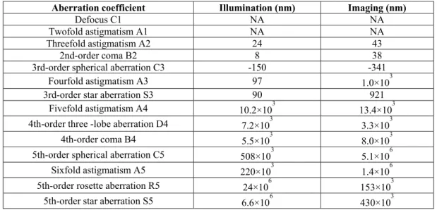
STEM image of GaN in [211] orientation shows the 63 pm distance Ga dumbbells clearly resolved. Tab. 2.1 gives a list of the typical residual aberration coefficients of TEAM 0.5 for operation at 300 kV from Kisielowski et al. [18]. A detailed account of the aberration coefficients and the aberration function can be found in Ref. [17].
Table 2.1 Typical residual axial aberration coefficient of the illumination aberration corrector and the imaging aberration corrector of TEAM 0.5 for operation at 300 kV. First-order aberrations, C1,and A1 are manually optimized (Kisielowski et al. [18])
Aberration coefficient Illumination (nm) Imaging (nm)
Defocus C1 NA NA
Twofold astigmatism A1 NA NA
Threefold astigmatism A2 24 43
2nd-order coma B2 8 38
3rd-order spherical aberration C3 -150 -341
Fourfold astigmatism A3 97 1.0×10³
3rd-order star aberration S3 90 921
Fivefold astigmatism A4 10.2×10³ 13.4×10³ 4th-order three -lobe aberration D4 7.2×10³ 3.3×10³
4th-order coma B4 5.5×10³ 8.0×10³
5th-order spherical aberration C5 508×103 5.1×10⁶ Sixfold astigmatism A5 220×103 1.4×10⁶ 5th-order rosette aberration R5 24×106 153×103 5th-order star aberration S5 6.6×10⁶ 430×103
In this study, I have used three transmission electron microscopes:
• JEOL 2010 LaB6: Operated at 200 kV, mainly used for conventional observation, such as low
magnification in plan-view, two beam and weak beam observation.
• JEOL 2010 FEG: 200 kV High Resolution TEM with a maximum point resolution of 0.19 nm (the Cs=1.4 mm for HRTEM), coherent illumination due to the FEG. This microscope was
used in this work for high resolution imaging.
• Titan 80-300 cubed: 300 kV High Resolution TEM equipped with an objective spherical aberration corrector at Institute of Physics of the Polish Academy of Sciences, Warsaw. This microscope was used for imaging the atomic structure of the misfit dislocation by HRTEM and HAADF (the Cs=0.001 mm for HRTEM, Cs=1.2 mm for HAADF, and Cc =1.4 mm).
23
2.2.2 TEM sample preparation
Plane-view and cross-sectional samples were prepared for TEM, HRTEM, and HAADF investigations. For the cross-sectional samples, slices of (1.5~2) x 5 mm2 were cut from the substrate side along the
[110] and [110] directions. Two slices were glued face to face and packed in copper tube of 3 mm in diameter with the epoxy glue, and then the tubes were cut into disks of about 800 μm in thickness. The procedures are illustrated in Fig. 2.6. The disks were then mechanically polished and dimpled from both sides until the thickness of the central area was about 10 μm. The final thinning was performed by argon ion milling at -150 oC in order to minimize ion beam damage. For the plane-view observation,
samples were cut into 3x3 mm2 and polished, dimpled and ion milled from the substrate side.
Figure 2.6 Procedure for preparing 3 mm disks of cross-sectional samples: (a) and (b) cut the sample into slices along [110] and [110] directions; (c) glue the slices face to face and form a sandwich structure; (d) and (e) pack the sandwich structure in the copper tube; (f) cut the tube into 3mm disks of 0.8 mm thickness.
2.3. Modes of operation and theoretical background
In this section some of the general techniques of electron microscopy as well as their theoretical background used in this work are summarized.
2.3.1 Diffraction
When it comes to diffraction, two concepts need to be considered: kinematical and dynamical diffraction. In kinematical diffraction single scattering is dominating; this is valid for very thin samples only. For dynamical diffraction, multiple scattering events occur as the electron pass through the sample. In this case, some electrons are even said to be absorbed due to repeated inelastic scattering events which send those electrons out of the main beam. Also, the incident and scattered
beams are coupled as multiple diffraction can contribute to the incident beam. The distribution of diffracted electrons in reciprocal space is referred to as the diffraction pattern and can be analyzed to determine the crystallinity and structure of the sample. When it comes to dynamical diffraction the relative intensity of the diffraction spots will change with sample thickness and atomic number, Z. For diffraction due to crystalline, the Bragg condition [19] must be fulfilled. This means that constructive interference of diffracted electron waves occurs at the Bragg angle, θB.
Another specific case of diffraction observed in this work is double diffraction, as shown in Fig. 2.7. This process occurs when the electron beam is rediffracted by a second crystal of different orientation and/or structure than the first crystal. This generates satellite spots in the diffraction pattern since the resultant diffraction vector depends on the combination of vectors from the two crystals. The relative position of the two crystals can be determined based on the appearance of the diffraction pattern. In so-called crystal-2 patterns the upper crystal gives the main diffraction spots while the lower crystal corresponds to the satellite spots [20]. But the opposite relationship has also been found [21]. The latter case is referred to as the top-bottom effect and can be attributed to dynamical diffraction effects, where the size of the deviation parameter causes the strongest diffracting spots to be arranged around the spot of the lower crystal.
Figure 2.7 (a) The selected area electron diffraction (SAED) pattern of GaSb island on GaP substrate. The different color spots show classification of the (220) diffraction, green, red and yellow spots are corresponding to GaP, GaSb, and double diffraction (DD), respectively. (b) [001] bright field image showing the (220) and (220) moiré fringes [22].
Double diffraction is very often accompanied by Moiré fringes in the corresponding TEM image as a consequence of interference between two different periodically spaced structures [20]. Depending on
25 the relative orientation of the spacings different Moiré fringes types are observed. Parallel fringes of two overlapping structures cause translational Moire fringes where the new spacing, dtm is related to
the respective spacings de and ds of the epitaxial material and substrate.
s e s e tm d d d d d − = (2.1)
Here I show an example that the moiré fringe patterns is applied to investigate the strain relaxation of an individual island. Applying this equation to a relaxed GaSb on GaP, the ideal spacing D{110} is 1.83
nm. As shown in the Fig. 2.7 (b), the [110] and [110] direction show different Moiré fringe spacing, indicating an anisotropic strain relaxation in the two directions [22].
2.3.2 Bright, dark and weak beam images
In the bright field (BF) mode of the TEM, as shown in Fig. 2.8 (a), an aperture is placed in the back focal plane of the objective lens which allows only the direct beam to pass. In this case, the image results from a weakening of the direct beam by its interaction with the sample. Therefore, mass-thickness and diffraction contrast contribute to image formation: thick areas, in which heavy atoms are enriched, and crystalline areas appear with dark contrast. In dark field (DF) images (Fig. 2.8 (b)), the direct beam is blocked by the aperture while one or more diffracted beams are allowed through the objective aperture. Since diffracted beams have strongly interacted with the specimen, very useful information is present in DF images, e.g., about dislocations, stacking faults or particle size.
Figure 2.8 Comparison of the use of an objective aperture in TEM to select (a) the direct and (b) the scattered electrons forming BF and DF images, respectively.
Figure 2.9 (a) The [001] zone axis diffraction patterns of GaSb islands on GaAs. (b) [001] bright field image showing the (220) and (220) moiré fringes. WBDF images of the same area recorded with different reflections of : (c) g = 040, (d) g= 220, and (e) g= 220.
Weak beam (WB) images refer to formation of a diffraction-contrast image in either BF or dark field (DF) where the useful information is transferred by weakly excited beams. The DF approach has been more widely used; because it gives strong contrast of the defects. In principle, the WBDF technique is an on-axis dark field imaging method by using a diffracted beam with large excitation error for the defect-free sample area. Thus, the defect free sample area appears dark because of the weak diffraction intensity. However, close to the dislocation core the hkl planes are bended back into the Bragg condition, which gives rise to a bright intensity peak (the dislocation line). The main challenge is to

![Figure 1. 3 Plot of cut-off frequency versus dc power dissipation form [17] that compares the rf performance of scaled n-channel InSb and Si devices](https://thumb-eu.123doks.com/thumbv2/123doknet/12732727.357340/17.918.279.636.425.708/figure-frequency-versus-dissipation-compares-performance-channel-devices.webp)

![Figure 2.1 A simple sketch showing the main components and rough layout and concept of MBE growth chamber [3]](https://thumb-eu.123doks.com/thumbv2/123doknet/12732727.357340/30.918.317.610.166.539/figure-simple-sketch-showing-components-layout-concept-chamber.webp)
![Figure 2.2 The schematic comparison of a optical (a) and electron (b) microscopy [4].](https://thumb-eu.123doks.com/thumbv2/123doknet/12732727.357340/31.918.257.661.466.736/figure-schematic-comparison-optical-electron-b-microscopy.webp)
![Figure 2.5 TEAM 0.5 STEM and TEM performance [18]. (a) HAADF image of wurtzite GaN [211]; crystal structure shown in the inset indicates Ga dumbbell spacing of 63 pm in this projection](https://thumb-eu.123doks.com/thumbv2/123doknet/12732727.357340/34.918.187.744.716.903/figure-performance-wurtzite-crystal-structure-indicates-dumbbell-projection.webp)