HAL Id: tel-01161948
https://tel.archives-ouvertes.fr/tel-01161948
Submitted on 9 Jun 2015
HAL is a multi-disciplinary open access
archive for the deposit and dissemination of sci-entific research documents, whether they are pub-lished or not. The documents may come from teaching and research institutions in France or abroad, or from public or private research centers.
L’archive ouverte pluridisciplinaire HAL, est destinée au dépôt et à la diffusion de documents scientifiques de niveau recherche, publiés ou non, émanant des établissements d’enseignement et de recherche français ou étrangers, des laboratoires publics ou privés.
Engineering of the light elements in silicon for the
photovoltaic application
Dilyara Timerkaeva
To cite this version:
Dilyara Timerkaeva. Engineering of the light elements in silicon for the photovoltaic applica-tion. Computational Physics [physics.comp-ph]. Université Grenoble Alpes, 2015. English. �NNT : 2015GREAY010�. �tel-01161948�
THÈSE
Pour obtenir le grade de
DOCTEUR DE L’UNIVERSITÉ DE GRENOBLE
Spécialité :Physique des matériaux
Arrêté ministériel : 7 août 2006
Présentée par
Dilyara TIMERKAEVA
Thèse dirigée parPascal POCHET et codirigée parDamien CALISTE
préparée au sein Laboratoire de simulation atomistique et deL’école doctorale de physique de Grenoble
Ingénierie des éléments légers
dans le silicium pour applications
photovoltaïques
Thèse soutenue publiquement le 10 avril 2015, devant le jury composé de :
Dr. Noël JAKSE Président Dr. Guy TRÉGLIA Rapporteur Dr. Laurent PIZZAGALLI Rapporteur Dr. Pascal POCHET Examinateur Dr. Damien CALISTE Examinateur Dr. Claudio ATTACCALITE Examinateur
Résumé
Depuis des années, le silicium est le semiconducteur principalement utilisé dans l’industrie électronique et photovoltaïque. Intensivement étudié depuis plusieurs décennies, ses propriétés sont essentiellement connues, mais de nouvelles questions viennent se poser. En particulier, une meilleure connaissance des nombreux défauts et impuretés ainsi que leurs propriétés et leur impact sur les performances des dispositifs à base de Si est souhaitable.
Ce travail couvre un éventail de problèmes liés aux défauts ponctuels en interaction au moyen de calculs dits de premiers principes (Density Functional Theory).
Une première partie est dédiée à l’impact du dopage sur la diffusivité de l’oxygène interstitiel. Les coefficients de diffusion obtenus en fonction de la température sont en très bon accord avec les résultats expérimentaux ce qui démontre la validité de la méthodologie appliquée. Nous avons montré que l’augmentation de la diffusivité dans le silicium dopé bore se produit par un mécanisme de transfert de charge depuis le dopant de type p.
Une deuxième partie se rapporte aux différents complexes de défauts ponctuels et leur thermodynamique, leur cinétique, et leurs propriétés optiques. La formation de ces complexes peut être induite expérimentalement par une irradiation par des électrons. Plus généralement, ils apparaissent aussi dans des environnements opérationnels particuliers comme le spatial. Ici, nous avons réalisé une étude expérimentale et théorique combinée pour identifier l’impact du dopage isovalent (C, Ge) et du co-dopage (C-Ge, C-Sn, C-Pb) sur la production de différents complexes (VOi, CiOi,
CiCs), qui sont électriquement et optiquement actifs.
Enfin, une attention particulière a été portée à la paire de défaut carbone-carbone et ses propriétés. Récemment, il a été établi que le silicium fortement dopé en carbone présente des propriétés d’émission laser. Ici nous avons cherché à étudier les formes possibles du complexe et leurs propriétés, afin de comprendre lequel est présent expérimentalement.
Abstract
Since many years, silicon is the primary semiconductor material in electronic and photovoltaic industry. Intensively studied through decades, its properties are essen-tially known, however new questions keep arising. We need to achieve deep insight into the numerous possible defects and impurities properties as well as their impact on the performances of the Si based devices. This work covers a range of problems related with point defects interaction of both types long range and short range by means of parameter free first principles calculations.
The former refers to the impact of heavy doping on diffusivity of interstitial oxygen species. The obtained diffusion coefficients as a function of temperature are in a very good agreement with experimental results that demonstrates the validity of the applied methodology. We showed that the enhanced diffusivity in B-doped silicon occurs through a charge transfer mechanism from the p-type dopant
The latter accounts for the various point defect complexes and their thermo-dynamic, kinetic, and optical properties. Formation of these complexes can be induced by electron irradiation of Czochralski silicon. This aspect is of extreme importance for particular operational environment. Here, we performed a combined experimental-theoretical investigation to identify the impact of isovalent doping (C, Ge) and co-doping (C-Ge, C-Sn, C-Pb) on the production of different complexes (VOi, CiOi, CiCs, etc.), which are electrically and optically active.
Finally, particular attention is addressed to the carbon-carbon defect pair and its properties. Recently, it was established that heavily carbon doped silicon elucidates lasing properties. Here we aimed to revisit the possible forms of the complex and their properties, in order to associate one of them with light emitting G-centre, observed in experiments.
Acknowledgements
Firstly, I would like to thank my supervisor, Dr. Pascal Pochet, for his guidance and support throughout these three years. Also my special thanks go to Damien Caliste, Thierry Deutsch, and Claudio Attaccalite, who have contributed much towards my progress and understanding.
I am very thankful for our experimental collaborators, in particular Charalampos Londos, Sébastien Dubois and their groups. I am also grateful to everyone who contributed to the BigDFT code development.
I thank all the members of L_Sim lab, in particular Paul Boulanger, Laura Ratcliff, Luigi Genovese, Frédéric Lançon, Yann-Michel Niquet, Gilles Brenet, Alex Marchenko, Maxime Moriniere, Alessandro Cerioni, Ivan Duchemin, Stephan Mohr, Jing Li, Elena Zvereva, Eduardo Machado-Charry.
This thesis couldnot be possible without my lovely friends, who have made my stay in Grenoble brighter and filled my heart with lots of happy memories. In particular, I thank Emerson Vathonne, Anita Sarkar, Anna Wolnik, Izabela Petrykiewicz, Williams Savero Torres, Arpan Krishna Deb, Dibyendu Hazra, Anna Mukhtarova, Vadim Mukhtarov, Joanna Gorniak, Joanna Andrecka, Pan Chen, Tatiana Krishtop, Vladimir Maryasin, Valeria Maryasina, Olesia Danyliv, Oleksandr Nechyporchuk, Andrey Eliseev. I also appreciate support of my old friends, Olga Fedorovich, Diana Bukaeva, Maria Kraynova, Niyaz Beysengulov, Bulat Fattakhov, Ildar Fattakhov. Apologies and thanks to those who were not specifically mentioned, but equally contributed to my happiness during that period.
For their constant support, encouragement, and being always there, I thank my dearest family - to whom I dedicate this thesis.
Contents
1 Introduction 1
2 State of the Art 5
2.1 Origin of impurities and point defects in silicon . . . 5
2.1.1 Silicon alloys used for the crystal growth: silicon grades . . . . 6
2.1.2 Crystalline silicon growth methods . . . 7
2.1.3 Specific operational environment . . . 8
2.2 Defects classification . . . 9
2.2.1 Extrinsic point defects (Impurities) . . . 9
2.3 Problematics . . . 12
2.3.1 Inter-defect interactions . . . 12
2.3.2 Oxygen kinetics in heavily doped silicon . . . 12
2.3.3 Secondary radiation defects in Cz-Si . . . 16
2.3.4 Secondary radiation defects in isovalently doped silicon . . . . 18
2.3.5 Optical properties of C-C complex: G-center . . . 20
2.4 Summary . . . 22
3 Computational Methodology 25 3.1 Density Functional Theory related concepts . . . 25
3.1.1 Schrödinger equation and Hartree-Fock Theory . . . 26
3.1.2 Density Functional Theory . . . 27
3.1.3 Exchange-correlation functionals . . . 29
3.1.4 Pseudopotentials . . . 30
3.1.5 Choice of a basis set . . . 30
3.1.6 Geometry optimization algorithms . . . 33
3.2 DFT for point defects studies . . . 35
3.2.1 Boundary conditions . . . 35
3.2.2 Chemical potential . . . 36
3.2.3 Binding energy . . . 36
3.3 Frequencies calculations . . . 36
3.3.1 The frozen-phonon approximation . . . 37
3.3.2 Frequencies of the bulk silicon . . . 37
3.3.3 Frequencies spectra for the defected structure . . . 41
4 Impact of heavy doping on structural and diffusion properties of oxygen impurity 43 4.1 Method . . . 44
4.2 Oxygen diffusion in low-doped material . . . 46
CONTENTS
4.4 Doped silicon . . . 55
4.4.1 Charge transfer mechanism . . . 59
4.4.2 Discussion on effect of doping on oxygen diffusivity . . . 62
4.5 Mechanisms of enhanced and retarded oxygen diffusion . . . 65
4.6 Conclusions . . . 66
5 On carbon doped and isovalently co-doped electron irradiated sili-con 69 5.1 Introduction . . . 69
5.2 Experimental data . . . 70
5.2.1 Carbon-poor and carbon-rich samples. Impact of carbon on irradiation caused defects . . . 71
5.2.2 Carbon-germanium co-doped silicon samples . . . 75
5.2.3 Carbon-lead co-doped silicon samples . . . 75
5.2.4 Discussion and analysis of experimental data . . . 76
5.3 Theoretical investigation of secondary radiation induced defects in carbon doped and isovalently co-doped silicon . . . 78
5.3.1 Carbon containing silicon . . . 80
5.3.2 Isovalently co-doped silicon . . . 83
5.3.3 Missing complexes . . . 88
5.4 Summary and conclusions . . . 94
6 Optical properties of the C-C defect in silicon 97 6.1 Introduction . . . 97
6.2 Method . . . 99
6.3 Results . . . 101
6.3.1 Discussion and conclusion . . . 106
7 Conclusions and perspectives 109 A Total energy values for the point defects and defect complexes 113 B List of publications and conference contributions 115 B.1 Publications . . . 115
Chapter 1
Introduction
Since many years, silicon is the primary semiconductor material in electronic and photovoltaic (PV) industry. It withstands the competition with new materials which show better performances in a range of properties. Compare to other materials, the main advantages of silicon are its cheapness and the existence of developed fabrication technologies. As a result, the semiconductor industry is well suited to the production of silicon based devices, such as silicon based integrated circuits and solar cells. In 2013, 90% of the total PV world production were based on the Si-wafers [124].
Intensively studied through decades, silicon properties are essentially known. However, industrial needs introduce new challenges: we now need small, high-performant, and in the meantime, cheap devices.
The latter criterion becomes the driving force for the modern industry and science. As far as the fabrication of highly purified silicon is extremely expensive, cheaper techniques are often used. As a result, we deal with silicon that contains impurities, intrinsic point defects, and dopants. The latter are added in silicon to vary the conductivity type. Types and quantities of defects presented in silicon depend on the growing method, compound of the initial melt, and the post-growing treatment, including irradiation and ion implantation. Hence, we need to achieve deep insight into the numerous possible defects and impurities properties as well as their impact on the performances of the Si based devices.
Among all the variety of impurities, oxygen is natively present in silicon during the crystal growth. Individual atoms of oxygen are electrically inactive, however they associate with each other and with other impurities. The resulting complexes sometimes affect significantly electrical and photovoltaic properties of future devices. Two examples are listed below. First, heating the silicon sample up to 450 ℃ leads to the formation of Thermal Donors (oxygen containing agglomerates). Second, under illumination, oxygen associates with boron, forming the so-called boron-oxygen complexes. Although the concentration of such complex is rather low 1011 cm−3,
CHAPTER 1. INTRODUCTION
its presence drastically degrade the solar cells efficiency. This effect is called Light Induced Degradation (LID). The complex’s composition and formation mechanism is still unknown, despite significant efforts performed in this direction [116, 12, 3, 43, 72, 134].
The first problem, that will be addressed in this thesis, is in close connection with the formation process of boron-oxygen complexes: we will investigate the oxygen migration mechanisms in doped silicon by means of parameter free first principles calculations. This problem raised from the recent observation of significantly en-hanced oxygen diffusivity in heavily B-doped silicon at low temperature regime
T < 700 ℃ [139]. The acceleration of oxygen diffusion in presence of boron can
thus accelerate the undesired defects formation. At the same time, the intensive doping with some other elements, namely Ge, As, and Sn, showed less prominent effect on oxygen migration properties. However, the mechanisms of enhanced or retarded diffusivity are not accessible through experimental techniques. That is why, we aimed to calculate the diffusion coefficient of the migrating oxygen species using the Density Functional Theory approximation.
Irradiation induced material properties is another aspect, closely related with point defects in silicon. This aspect is of extreme importance for particular operational environment. Either enhanced or reduced sensitivity to irradiation is required for a number of applications, such as dosimetry, particle detection, medical equipment, satellite and space station equipment. It is of a great importance to investigate point defect engineering techniques and strategies to master those properties through controlled defect manipulation. Therefore, in the second part of this work we investigate point defects associated with the electron irradiation.
A large variety of impurity associations occurs under electron irradiation. Vacan-cies and self-interstitials interact with impurities that results in complexes formation. Some of those act as recombination centers and reduce electrical characteristics of future devices. In order to avoid their formation, two solutions are possible. The first one consists in using the impurity-free silicon. In the absence of impurities, any associations will be impossible. However, this solution requires an expensive purification method. The second one consists in finding a proper defect engineering strategy. For example, by adding electrically inactive impurities, we can intend to avoid the detrimental complexes formation in irradiated silicon. The best candidates for that role are isovalent dopants. Their impact on the hardening potential of silicon will be investigated in this thesis by employing combined experimental-theoretical methods.
Finally, the third aspect, that is addressed in this thesis, is the carbon-carbon defect pair and its properties. Recently, it was established that heavily carbon doped silicon elucidates lasing properties. The complex related to this feature is detected to
be CiCs complex. Three variations of the complex have been proposed in literature.
One of them is widely accepted to be related with light emitting G-centre, however no theoretical confirmation has been presented yet. Here we aimed to revisit the possible forms of the complex and their properties, in order to associate one of them with light emitting G-centre, observed in experiments.
The thesis will be organized as follows. In Chapter 2, we will represent the state of the art in the field of point defects in silicon, followed by the open questions which will be addressed in this thesis. In Chapter 3, we introduce the details of the theoretical methodology employed in the rest of the thesis. In Chapter 4, we present our results on the diffusion coefficient calculations of interstitial oxygen species in pristine and heavily doped silicon. Chapter 5 deals with irradiation induced point defects formation and temperature evolution in isovalently doped and co-doped silicon. Here, we present and analyze the experimental results, obtained by our Greek colleagues along with the multi-scale simulations, accounting for both thermodynamic and kinetic aspects of various point defects associations. Chapter 6 addresses the structural, thermodynamic, vibrational, and optical properties of the CiCs complex.
And finally, in Chapter 7, we draw conclusions of the present contribution along with perspectives in the field of point defects in silicon.
Chapter 2
State of the Art
This chapter addresses the state of the art in the field of point defects and impurities in silicon. We start by a short description of the origin of point defects in crystalline silicon. Then we classify the possible point defects and complexes in bulk silicon, depending on their origin and properties. We overview, how the performances of silicon-based devices are affected as by these point defects, as well as by their long-range and short-range interactions.
Particularly, we address the oxygen transport as it is responsible for the formation of electrically active thermal donors and B-O complexes. We summarize the recent experiments showing how heavy doping impacts the oxygen transport and specify the open questions.
The electron irradiation causes the formation of a large variety of defect complexes, which impact electrical, photovoltaic, and optical properties of crystalline silicon. This is the second point that we address in this chapter. We overview how electron irradiation affects the Czochralski silicon and emphasize the related questions. We also consider the impact of the isovalent co-doping on complexes formation in irradiation hardness of Czochralski silicon.
Finally, we discuss the irradiation induced CiCs complex. It rises the lasing properties of crystalline silicon. We overview the experimental and theoretical studies of its properties and point out the question of the possible complex configurations.
2.1
Origin of impurities and point defects in
sili-con
The quality of a silicon-based device considerably depends on the purity of the silicon crystal. The purity and the homogeneity are the main criteria of the crystal. However, in reality the crystal is never perfect. Three main sources of structural defects and impurities can be emphasized: 1) silicon alloy used for the crystal growth,
CHAPTER 2. STATE OF THE ART
2) crystal growing method, and 3) operational environment.
2.1.1
Silicon alloys used for the crystal growth: silicon grades
Industry deals with three silicon grades: Metallurgical grade (MG-Si), Electronic grade (EG-Si), and Solar grade (SoG-Si). Lets briefly consider each of the grades.
MG-Si is the alloy, extracted form the silica (SiO2) in an electric arc furnace. It is
a result of the chemical reaction SiO2+2C → Si+2CO, which occurs at temperatures
higher than 1990 ℃. It is 99% (silicon 2N = 2 Nines) pure. It contains impurities like SiO2, SiC, metals, dopants, and light elements and is, therefore, useless for the
electronic and photovoltaic applications. Depending on the required application, particular purification is followed.
EG-Si is the alloy obtained from MG-Si. The purification process includes the
gaseous phase of silicon. Several methods exist, among them, the "Siemens procedure" is the most popular. Very high temperature stages make this purification method extremely expensive. The purification includes the following reaction: Si + 3HCl → SiHCl3 + H2. The fractional distillation separates SiHCl3 from other components.
Occurring in the gaseous phase, the inverse reaction liberates Si. Si then crusts on the multi-crystalline bar. Resulting alloy is a 99,9999999% (9N) pure silicon. However, the cost of EG-Si is relatively expensive compare to SoG-Si.
SoG-Si is the alloy also obtained by purification of MG-Si. Contrary to the EG-Si,
gaseous phase is not involved in a process. The purification include the solid and the liquid phases only. The fabrication of SoG-Si from MG-Si involves a segregation and a plasma torch processing. The purity of the final material is much cleaner that in MG-Si, but much more dirty than EG-Si, and is fully determined by the quality of the cleaning steps.
The first step consists of the repeated melting and the controlled solidification of a silicon ingot. The crystal growing conditions and the affinities of the impurities with the solid and the liquid phase determine the concentrations of the impurities in the crystal. The impurities concentration in the liquid phase changes during the growth procedure. Hence, the impurities distribution along the crystal is inhomogeneous and characterizes by the segregation parameter. In thermodynamic equilibrium, it is determined as the ratio of the solubility of the impurity in solid, to its solubility in liquid: k0 = sS/sL. If k0 ≪ 1, the impurity essentially stays in the liquid phase.
Only the bottom part of an ingot contains more impurities of this type. It can be simply cut out. This is true for most metallic impurities (for ex. k0(Fe) = 8 · 10−6).
2.1. ORIGIN OF IMPURITIES AND POINT DEFECTS IN SILICON Impurity k0 Concentration [cm−3] B 0.8 > 1013 P 0.35 > 1013 O 0.25-1.25 ∼ 1016− 1018 C 0.07 ∼ 1016 Ge 0.33 NA Sn 0.016 NA
Table 2.1: The segregation parameter k0 for some silicon impurities and their
approximate concentrations in SoG-Si [57, 132].
2.1). The bigger is k0 of the particular impurity, the more important content of this
impurity will be in the crystal. In the general case, the thermodynamic equilibrium is unachievable. Thus the impurity concentration should be estimated by considering the effective segregation coefficient [18, 108]. However, the tendencies described above maintain essentially valid.
The second step, namely plasma torch processing, allows to remove some of the resting impurities after the segregation step. Despite these two purification steps, SoG-Si contains much more impurities than EG-Si: metals (Fe, Cr, Ti, etc), light elements (O, C, N, etc.), and dopants (B, P, Al, etc). Their approximate concentrations are given in Table 2.1. However, the advantage of the SoG-Si is its cheapness.
2.1.2
Crystalline silicon growth methods
The crystal growth follows the silicon alloy purification step. The crystal growth process can be another possible source of impurities and structural defects. The semiconductor industry deals with mono-crystalline, multi-crystalline, or mono-like silicon.
Monocrystalline silicon is usually grown by Floating Zone (FZ) or Czochralski
(Cz) method. The FZ-Si allows to obtain an excellent quality mono-crystalline ingot. An induction coil locally melts the silicon ingot and is gradually moved from its bottom to the top. The procedure can be repeated until the desired quality is reached. The FZ method allows obtaining an excellent crystal quality. The concentration of the oxygen and carbon impurities is less than 1016 cm−3. The principal impurity is
copper, which is introduced due to the contact of induction coil with the silicon. The second method is the Czochralski method [30, 127] and is one of the most widespread industrial method for the growth of the silicon mono-crystals. Silicon alloy is firstly melted in a quartz crucible (SiO2). The crystal growth starts when the seed rod is
CHAPTER 2. STATE OF THE ART
directions, while the rod is pulled from the melt. The quartz crucible slowly dissolves into the melt, releasing a large quantity of oxygen. Most of the oxygen evaporates from the melt surface as a SiO gas, while the resting 1% stays in the melt and dissolves into the ingot. After being evaporated, SiO interacts with a hot graphite susceptor and forms carbon monooxide (CO). CO dissolves back into the silicon melt from the surface. At the end of the process, one gets a cylindric single crystal silicon, which orientation is determined by the seed rod. The main impurities of the Cz-Si are oxygen and carbon. Their concentrations are determined by the segregation coefficient and is usually of the order of 1017− 1018 cm−3 for the oxygen impurity
and of the order of 1016− 1017 cm−3 for the carbon impurity [57].
Multicrystalline silicon 45% of the photovoltaic industry is based on
multicrys-talline silicon. The growth procedure is based on the controlled solidification of the silicon melt. Silicon alloy is put in a quartz crucible, covered by a silicon nitride (Si3N4) film. The latter reduces the oxygen incorporation to the melt from the
crucible. The film also limits crack formation in the crystal. However it is a source of metallic impurities [58]. Once the silicon is melted and become a homogeneous substance, the solidification is started. Solidification is driven by the cooling of the silicon from the bottom to the top until full solidification. The multi-crystal consist of grains of different shape and size. It contains less oxygen that the Cz-Si, about 2 − 3 · 1017 cm−3.
Mono-like silicon The mono-like technology allows growing silicon crystal with
large monocrystalline grains. The technology is based on the controlled bottom-top solidification of the crystal (as in the case of multicrystalline silicon). The difference is that we place one or several monocrystalline seeds on the bottom of the crucible. That allows producing big zones of mono-crystal. This growing method is cheaper than Cz-Si, although the quality is slightly reduced due to disclocations between monocrystalline zones and multicrystalline edges.
2.1.3
Specific operational environment
Particular operational environments can also lead to the formation of point defects in silicon. Often the semiconductor devices have to function in irradiation environments. For example, such conditions appear in the open space, during some medical procedures, or inside particle accelerators. The defect formation can be a desired effect, as in the case of particle detectors, or undesired, as in the case of the space or medical electronic devices. In particular, let us focus on the electron irradiation. This type of irradiation lead to a formation of a Frenkel pair. The Frenkel pair is made of a vacancy (V) and a self-interstitial (I), which are the intrinsic,
2.2. DEFECTS CLASSIFICATION
or structural, point defect of silicon. Both V and I are quite mobile and interact with impurities, forming a range of defect complexes.
Besides above discussed point defects origins, we consider one last way of their appearing. This is the deliberate introduction of an impurity. It can be realized through different techniques. In the case of dopants, desired elements can be introduced into an alloy before the growing process. It can be also done via ion implantations.
In the following section we will classify all these defects and briefly characterize them.
2.2
Defects classification
As it was previously summarized, it is hardly possible to avoid any kind of defects. The majority of the industrially produced silicon contains defects. Those can be structural defects (grain boundaries, dislocations, vacancies/interstitials) or impurities. All of them can affect the silicon’s properties: mechanical, transport, electrical, optical, and others. As a result, defects impact the quality of the future devices. The impact can be negative: for example, some defects act as recombination centers. But they can sometimes positively affect the semiconductor properties. The p- or the n-type dopings change the majority carrier type and they are oFften desired.
That is why it is extremely important to investigate their behavior and their impact on silicon properties. Point defects were intensively studied both theoretically and experimentally [36, 106]. However there are still some lacks related to point defects interactions, which we aim to address in this thesis.
However, prior to emphasize the range of problems in this area, we will summarize and classify the point defects and briefly introduce their properties. Table 2.2 classifies the point defects and impurities according to their origin and effect on the electrical properties.
2.2.1
Extrinsic point defects (Impurities)
We start our description by the native point defect. By native point defects we mean those, which appear in the crystal due to the growth techniques. This include light impurities, metals, and p-/n-type dopants. Then, the isovalent dopants and the electron irradiation induced defects will be also briefly discussed.
Light impurities, such as oxygen, carbon, and nitrogen, are electrically neutral.
However, by forming precipitates or defect complexes, they may directly affect silicon’s electrical properties. The term "light impurities" is chosen for them as
CHAPTER 2. STATE OF THE ART Ligh t Primary Secondary Asso ciations impurities Metals Dopan ts radiation radiation of iD with p-t yp e(pD) n-t yp e(nD) iso valen t (iD) def ects complexes radiat ion defects Oi F e B P C V (V2) V O DSi I O2i Cu Al As G e SiI V O2 Ti G a Sb Sn DI C Co Pb V2O H Ni V2O2 DC Mo Au CiOi D V ... CiO2i CiOiI D V O CsOi CsO2i ... Ci CiCs CiCi T able 2.2: P ossible defect complexes are group ed b y their origin.
2.2. DEFECTS CLASSIFICATION
their atomic masses are lighter than that of silicon. C impurity also belongs to the isovalent impurities group.
Metals introduce deep energy levels, close to the middle of the band gap. That
is why they act as recombination centers. As a result, the metal impurities reduce free carrier lifetime in photovoltaic or microelectronic devices. Metallic defects can occupy substitutional or interstitial positions. Most of the metal elements can be excluded from the crystal via repeated segregation technique. The resting metallic elements can be eliminated by the so-called internal gettering process [4]. In other words, oxygen precipitates capture and deactivate the metallic impurities, so that there is less of them in the active crystalline zone.
p- and n-type dopants are highly soluble in silicon crystal (in solid phase of
silicon). They usually substitute the silicon atoms in the crystal sites. Being the elements of the III and V column of periodic table, they significantly affect semiconducting properties of the silicon by introducing shallow levels in the band gap. p-type dopants consist of B, Al, and Ga, while n-type dopants consist of P, As, and Sb. B and P are the most widely used dopants, as far as they are naturally present in important concentrations in the MG-Si. These elements are often desired as they lead to a certain conductivity type. However, their presence causes sometimes to detrimental effects. For instance, B presence leads to a Light Induced Degradation (LID) of the solar cells [12].
Isovalent dopants include the elements of the IV column of the periodic table,
namely C, Ge, Sn, and Pb. Usually, these elements occupy a substitutional position in the crystal. As far as they have four valence electrons they are electrically neutral. Hence, they introduce no levels in the band gap and do not affect the carrier lifetime. However, these elements’ sizes differ from that of silicon. As a result, they introduce long-range elastic fields. Their presence in significant concentration of > 1020 cm−3
changes the cell parameter of the silicon crystal. Similar to the light impurities, they are electrically neutral, but they can form electrically and optically active complexes when associated with other impurities and point defects.
Irradiation induced defects The most important irradiation induced point
de-fects are vacancies and self-interstitials. They can be introduced in small quantities during the growth process. However, electron irradiation may cause their presence in significant concentrations. In this thesis we will consider the electron irradiation induced defects. We classify them into two subgroups, namely primary and secondary radiation defects. The primary radiation defects are vacancies and self-interstitials.
CHAPTER 2. STATE OF THE ART
The secondary radiation defects are the whole range of possible combinations of primary radiation defects with each other and with other impurities.
In this section, we have summarized and structured the point defects and point defect complexes in crystalline silicon. From now, we start the discussion in more detail the problematics, that will be treated in the present thesis.
2.3
Problematics
2.3.1
Inter-defect interactions
The defects intensively interact with each other. One can conventionally distin-guish 2 types of interaction: short-range and long-range interactions.
A defect complex is formed as a result of the short-range interaction. The complex is a localized defect and its properties usually differ from the properties of its components. Each complex affects the crystal properties in its own way. For example, most of the secondary electron irradiation induced complexes introduces deep levels in the bandgap. VOi and CiOi are thought to act as recombination centers
and thus can lead to a severe degradation of the electronic device properties [16, 61]. As a result of the long-range interaction, no complex is formed. The interaction happens through the long-range fields, such as electric, elastic, and magnetic fields. The defects properties, their behavior, and the way they affect silicon, can be modified. For example, the solubility of the lead (Pb) atoms in silicon can be increased by carbon (C) incorporation.
In this work we deal with both long- and short-range interaction types. The change in oxygen kinetics properties is an example of the long-range interaction, while the secondary radiation induced complexes are examples of the short-range interaction. In the resting part of this chapter, we point out the background and the open questions related to the two interaction types. We organize the background information and open questions in the order they appear in the next chapters. The titles of the chapters reflect the titles of the background items. Here, we will mostly focus on the experimental aspects of the problems, while the necessary methodological and theoretical insights are given in the methods and the results chapters, respectively.
2.3.2
Oxygen kinetics in heavily doped silicon
Oxygen is a particular impurity, as it is almost always presented in crystalline silicon in concentrations of 1016− 1018 cm−3 [95]. Its impact on silicon-based devices
is ambiguous. On one hand, it does not affect the electrical properties of silicon and improves the mechanical strength of the crystal; oxygen precipitates getter the
2.3. PROBLEMATICS
(a) Oi (b) Oi2
Figure 2.1: The schematic geometry configuration of oxygen monomer (a) and dimer (b).
undesired metallic impurities [128]. On the other hand, the so-called Thermal Donors [51] are related to the oxygen agglomerates formation; some oxygen containing defects (such as V-O, C-O, B-O complexes) act as a recombination centers and reduce the solar cells efficiency [12, 119]. Famous boron oxygen complex is responsible for the Light Induced Degradation of the solar cells [42, 116, 12, 134]. Both the exact composition of the defect and its formation mechanism are still discussed [2, 134, 116]. However, one can infer the importance of precise knowledge of oxygen diffusing properties for all mentioned phenomena.
The oxygen diffusivity depends on the temperature range, as well as on the concentrations of the dopants and the impurities presented in silicon. In low doped silicon, one can distinguish two temperature modes:
— high temperatures, above 700 ℃ and below the silicon melting temperature ∼ 1400 ℃;
— low temperatures, 300-700 ℃.
At the high temperatures, we observe the so-called normal˝ diffusion, which diffusion coefficient can be described by the following empirical expression [60]:
D(O) = 0.13exp(−2.53eVkT )cm2s−1. (2.1)
In this case, an interstitial oxygen monomer is the particle responsible for the oxygen transport (see Figure 2.1(a)).
At the low temperatures, an enhanced oxygen diffusion is observed. The enhance-ment was associated with an activation energy of 1.5 eV [70, 88, 117], whereas the dimer is thought to be the responsible diffusing species [46]. However, stress induced dichroism experiments, which is sensitive to only single oxygen atoms jumps, have shown that monomers diffusion coefficient is also described by the extrapolation of Expression (2.1) [60].
While the oxygen diffusivity is not affected by the low doping rates, it turned to be sensitive to heavy doping, when the dopant concentration is equal or greater than
CHAPTER 2. STATE OF THE ART
that of oxygen [93, 139, 138]. Gathered during the past two decades, the number of experimental evidences had revealed certain trends, summarized in Table 2.3. Let’s consider the reported effects of p-type, n-type, and isovalent dopants on the oxygen diffusivity one by one.
p-type doping. At the low temperatures, experiments show sometimes
contradic-tory trends. Most of the studies suggests the enhanced oxygen diffusion in heavily doped p-type silicon. The first indirect evidence was the observation of an enhanced Thermal Donors formation, as reported by Wada et al [136]. Recent Dislocation Locking (DLT) experiments suggest an oxygen transport increase by a factor of at least 8 [139, 93], compared to low doped material. An enhanced kinetics of oxygen precipitation [138], which occurs in heavily B-doped material, also supports the evidence of the enhanced oxygen diffusivity. However, some earlier Secondary Ion Mass Spectroscopy (SIMS) outdiffusion profiles showed a reduced diffusivity in heavily B-doped samples at 600-800 ℃ by a factor of 2 to 5 [126]. At high tempera-tures, B-doping leads to either very weak or no impact on the oxygen diffusion and precipitation kinetics [99, 138].
n-type doping. There are few evidences of the reduced oxygen diffusion in the
heavily n-type doping in the low temperature range. Phosphorus doping reduces the thermal donors formation, according to Wada et al [136]. Both the heavily arsenic-doped and the antimony-doped samples slow the oxygen diffusion, as revealed by Takeno et al [126], by increasing its migration energy by 0.64-0.68 eV and 1.4 eV, respectively. Dislocation locking experiments show the slowing of the oxygen diffusivity by a factor of 5 in the heavily As-doped silicon [139]. However, no dependence of the diffusivity was found in the antimony doped silicon with the DLT experiment [93].
Isovalent doping. Doping with germanium slows the oxygen diffusivity by the
factor of 4 according to Zeng et al. in the low temperature range [139]. As far as the Stress Induced Dichroism (SID) technique is only sensitive to the oxygen monomer diffusion, it was shown that the increasing germanium content is slowing more the monomers diffusion at 375 ℃ [62].
To summarize, p-type, n-type, and isovalent doping have an impact on the oxygen diffusivity at the low temperatures. As it was earlier concluded in Reference [139], experimental evidences suggest that both internal strain and change in Fermi energy level can cause the changes in kinetic properties of oxygen. For example, high germanium content introduces relatively important change in the lattice parameter (∆aa = +7 × 10⁻⁵) of silicon without affecting its electrical properties, while high
2.3. PROBLEMATICS Dopan t Concen tration [cm − 3 ] T emp erature Effect on oxygen transp ort T ec hnique and sensitivit y References B 8. 0 · 10 18 to 1. 2 · 10 19 1050 ℃ None SI MS -effectiv e [99] B 8. 0 · 10 18 to 1. 2 · 10 19 800 ℃ Slo ws (factor of ∼ 5) SIMS -effectiv e [99] B 4. 4 · 10 18 500 and 800 ℃ None SI MS -effectiv e [126] B 4. 4 · 10 18 600 to 700 ℃ Slo ws (factor of ∼ 5to 3) SIMS -effectiv e [126] B 2. 7 · 10 18 to 8. 0 · 10 18 350 to 550 ℃ Enhances (factor of ∼ 40) DL T -effectiv e [93] B 30 .· 10 18 350 to 550 ℃ Enhances (factor of ∼ 8to25) DL T -effectiv e [139] G e 1. 0 · 10 16 to 1. 0 · 10 20 1050 to 1200 ℃ Enhances SIMS -effe ctiv e [23] G e 5. 0 · 10 20 to 2. 7 · 10 21 375 ℃ Slo ws (more with increasing [G e]) SIMS -effectiv e [62] G e 8. 0 · 10 19 400 to 700 ℃ Slo ws (factor of ∼ 1. 25to3 .3 ) D L T -effec tiv e [139] As 1. 1 · 10 19 1050 ℃ None SID -monomers [99] As 1. 1 · 10 19 800 ℃ Slo ws (factor of ∼ 2. 5) SIMS -effectiv e [99] As 4. 0 · 10 18 to 1. 3 · 10 19 400 to 700 ℃ Slo ws (E a increased b y 0.64 to 0.68 eV) SIMS -effectiv e [126] As 2. 0 · 10 19 400 to 700 ℃ Slo ws (factor of ∼ 1. 1to5) DL T -effectiv e [139] Sb 5. 0 · 10 20 to 2. 7 · 10 21 950 to 1100 ℃ None SI MS -effectiv e [100] Sb 5. 0 · 10 17 800 to 1050 ℃ None SI MS -effectiv e [99] Sb 1. 3 · 10 18 600 to 800 ℃ Slo ws (E a increased b y 1.40 eV) SIMS -effectiv e [126] Sb 8. 0 · 10 17 450 to 550 ℃ None DL T -effectiv e [93] T able 2.3: Rep orted effects of high t concen tration of various dopan ts on the transp ort of oxygen in Cz-Si [139 ]. W e denote SIMS: Secondar y Ion Mass Sp ectroscop y; DL T: Dislo cation Lo cking T ec hnique; SID: St ress Induced Dic hroism.
CHAPTER 2. STATE OF THE ART
content of the p- and n- type dopants change the Fermi energy level of the crystal. As it was reviewed above, both cases are known to impact the oxygen diffusivity properties.
It is also evident, that experimental techniques employed to measure the diffusivity has a significant impact on the obtained trends. That is why additional studies are necessary to decipher the underlying mechanisms of enhance or retarded diffusion of oxygen species in the silicon crystal.
Significant efforts were made in order to understand the mechanisms lying behind the observed changes in oxygen diffusivity. For example, other diffusing particles, such as VO, IO, molecular O2 [47], chains of more than 3 interstitial oxygens [71],
were proposed as a diffusing species. It was shown that they can barely be involved in oxygen transport [29, 125]. Dimers diffusion in doubly charged state is an alternative possibility for an enhanced transport proposed by Adey et al [3, 37]. However, no signs of charged dimers were yet observed [92]. Another explanation for the enhanced diffusion is the so-called Bourgoin-Corbett mechanism [13, 14, 101]. Such mechanism is based on the fact, that the ground state configuration of the neutral oxygen dimer becomes the saddle point of the doubly charged state, whereas the saddle configuration of the neutral dimer becomes the ground state. The mechanism suggests that the oxygen dimer captures and releases one or two electrons and diffuses with a very low activation barrier or even nearly barrierless, which contradicts the experimental observations [46, 93, 139].
To summarize, no satisfactory explanation has been yet proposed for the enhanced and retarded oxygen diffusion in heavily doped silicon. That is why we aimed to investigate this aspect and decipher the enhanced-retarded mechanisms of the oxygen diffusion in heavily doped silicon.
2.3.3
Secondary radiation defects in Cz-Si
The second particular topic, that is discussed in this thesis is the irradiation induced defects in Cz-Si. The principle damage caused by electron irradiation is the formation of a Frenkel pair. The Frenkel pair consists of a silicon self-interstitial (I), the silicon atom knocked off from its formal position, and the resulting vacancy (V). Those are primary radiation defects (see Table 2.2 Column 6). In the course of the irradiation, more and more Frenkel pairs are formed. The vacancies and the self-interstitials diffuse and promptly interact with other point defects and impurities. Those are secondary radiation defects (see Table 2.2 Column 7).
As it was already mentioned, Cz-Si contains oxygen and carbon impurities, which are introduced in the crystal during the growth process. During the irradiation course, the primary radiation defects will thus interact with these impurities. Once
2.3. PROBLEMATICS
the vacancy encounters an oxygen, they bind together and form vacancy oxygen complex (VO), the so-called A-center. The self-interstitials rather interacts with a carbon atom and form the fast-diffusing carbon interstitials (Ci). Ci diffuses through
the crystal until it encounters an oxygen or a substitutional carbon and forms carbon oxygen CiOi or carbon-carbon CiCs complex. Thus, the concentration of these
complexes depends on the irradiation time, the temperature, and the impurities concentrations. Moreover, further interactions of the primary radiation defects with these complexes produce bigger aggregates, consisting of three or more compound atoms.
The complete understanding of the electron irradiation induced complexes is of extreme importance. Firstly, the irradiation damage together with the implantation of certain dopants and impurities allows producing material with specific characteristics. Secondly, it provokes the formation of the defects and complexes in considerable concentrations. That makes them visible for experimental techniques. Finally, the radiation induced complexes are of extreme importance for the applications operating in specific environments. The list of such applications includes: dosimetry, particle detection, medical equipment, satellite equipment, and space station equipment.
Among the range of experimental techniques, the infrared (IR) absorption [6, 48] is the most suitable technique for the point defects identification. It allows identifying defects through their Localized Vibrational Modes (LVM), set of which are unique for each defect and sometimes referred as vibrational fingerprints. The concentration of the defect is proportional to the intensity of the related band. The proportionality coefficient kcal has to be calibrated for each defect using the cross-analysis with
other techniques. Table 2.4 lists the calibration coefficients for some defects of the irradiated Cz-Si. Defect IR band [cm−1] k cal[1017cm−2] References O 1106 3.14 [5] C 606 1.0 [114] VO 830 0.625 [33] VO2 0.313 [79, 73, 80] CiOi 860 1.1 [33] CiOiI (940;) 1024 0.38 [33] CiCs (B form) 544 (0.015)0.42 [67]
Table 2.4: The calibration coefficients for some point defects in irradiated Cz-Si. The irradiation induced point defects in Cz-Si have been widely studied. Most of related complexes are identified as well as their properties. Unfortunately, the full microscopic insight cannot be derived solely from the IR absorption experiments. The reasons for that is listed below.
CHAPTER 2. STATE OF THE ART
2. Even if the defect or a complex exists, its bands can be sometimes invisible. They can be shadowed by another band or can be out of the detection range or can be under the detection limit.
3. Superposition of two bands may obscure the obtained concentrations.
4. LVM of heavy point defects (heavier than the mass of silicon atom) are superposed with the vibrational frequencies of the bulk silicon.
Some of these difficulties can be overpassed employing theoretical simulations. However, there is still a lack of a precise and effective tool to describe and to predict the defect complexes formation and their temperature evolution in the irradiated material.
Theoretical description of the defect complexes formation and evolution requires three parameters:
— The formation energy, the energy to produce a defect, such as structural point defect(V or I) or charged particles.
— The binding energy of the complex, the energy gain when the two parts of a complex bind together.
— The migration energies of the components and the complex itself, the energy of the barrier, that a species need to overpass to reach the neighboring site. These parameters can be calculated with ab initio methods. However, the further analysis is required to investigate the competitive processes and temperature evo-lutions. Two most frequently used methods are the Monte Carlo (MC) and the Mass Action Law (MAL) techniques. MC provides a precise kinetic picture, however requires a significant amount of time and computational sources. The second is fast and effective, but only describes the thermodynamic equilibrium and misses the kinetic aspects. The third method is the kinetic mass action law (KMAL). KMAL combines the advantages of both techniques, and is able to provide the temperature evolution of point defects by taking into account both thermodynamic and kinetic aspects.
In this work, we aimed to perform the mixed experimental and multi-scaled theoretical analysis of the irradiated Cz-Si. The theoretical results will be compared with the results of the IR experiments.
2.3.4
Secondary radiation defects in isovalently doped
sili-con
As it was previously mentioned, some of the secondary irradiation complexes are undesired as they reduce the performances of electronic devices. For example, VO and CiOi complexes introduce deep levels in the silicon bandgap, which lead to a
2.3. PROBLEMATICS
as they enhance the performance of the Si-based devices. For example CiCs complex
can be used to obtain an optical gain and stimulated emission. That is why we do not necessarily need to suppress, but we rather need to control the defect complexes formation in Si.
The use of isovalent doping is a possible defect engineering strategy in order to achieve such a goal. Previously, number of IR absorption studies have been performed to investigate the impact of Ge, Sn, and Pb on irradiation caused defects [24, 25, 63, 75, 77, 78, 83, 81], therefore here we will introduce a short summary of most important trends in Ge, Sn, and Pb isovalently doped silicon. We will focus on the imact of isovalent doping on formation and thermal stability of main electron irradiation induced pairs, namely VOi, CiOi, and CiCs.
Ge doping. The Ge doping leads to an enhanced production of all three pairs, i.e.
VOi, CiOi, and CiCs [77]. While thermal stability of CiOi and CiCs complexes has
not been affected, that of VOi is found to be reduced [78]. In addition, the reduced
amount of VO complex is converted to VOi2 defects in Ge presence [79].
Figure 2.2: From reference [24].
Sn doping The Sn doping strongly impacts the VOi pairs formation in the electron
CHAPTER 2. STATE OF THE ART
suppressed in Sn-reach silicon sample during the irradiation course. However, the VOi pairs emerge upon isochronal annealing at the ∼ 200 − 350 ℃ temperature
range, but their concentration is significantly reduced compare to the Sn-poor Si.
Pb doping . The Pb doping have been studied by electrical measurements. The
measurements have suggested a partially suppressed production of both VOi and
CiCs pairs in the Pb doped silicon [31, 94]. However, the situation is less clear
concerning other aspects: the CiOi defect production and all three pairs stability
have not been investigated yet. No reports have been published on the VOi → VOi2
conversion ratio.
In this thesis, we aimed to perform a systematic investigation of the irradiated isovalently doped and isovalently co-doped silicon. This is why we aimed the systematic experimental insight by means of IR absorption experiments as well as exhaustive theoretical study of possible defect complexes by means of DFT calculations.
2.3.5
Optical properties of C-C complex: G-center
CiCs is one of the secondary irradiation induced defects. The pair is associated
to the light emitting G-center [8, 7]. The G-center is lasing at 0.97 eV (1280 nm) as illustrated in Figures 2.4 and 2.3. It was discovered in the 60’s as a by-product in the silicon crystal caused by the radiation damage from the bombardment with high energy electrons, ions and gamma rays. In recent years, an important effort has been made in order to increase the G-centers concentration [90, 8, 7]. The methods are generally based on the silicon surface alteration, followed by a laser annealing. These technologies have promising applications in development of a silicon laser.
The structure of the CiCs pair has been debated for almost 40 years. Its
config-uration has been investigated by experimental as well as by theoretical techniques [17, 98, 121, 67, 69, 22, 66]. The summary of the experimental and theoretical studies on carbon-carbon complexes is listed in Table 2.5.
Two forms of carbon-carbon complexes, namely A and B forms, have been identified experimentally. Their vibrational modes have been experimentally obtained and are listed in Table 2.5. The G-centre is thought to be the B form of the CiCs pair.
From the theory point of view, both A and B forms were found to be stable with a binding energy about ∼ 0.8 − 1.3 eV [87, 141, 35]. The localized vibrational modes have been reproduced for the neutral and charged states for both forms [35, 69, 22].
Despite the A and B forms of CiCss complex, there are one more experimental and
one more theoretical investigations, which suggest C-C pair configurations, different from both A and B forms.
2.3. PROBLEMATICS T ec hnique Prop ert y Main results References Exp erimen tal w orks EPR Structure 2C orien ted in h111 i in a V [17] ODMR Structure A-and B-forms [98] EPR, DL TS, PL Charged states A form is more stable than B form [121]+ refs. ther ein of A-and B-forms for all charge states, except neutral IR L VM A form: 594. 6, 596.9, 722.4, 872.6, 953.0 cm − 1 [67] B form: 540.4, 543.3, 579.8, 640.6, 730.4 and 842.4 cm − 1 EPR Configuration Conf. 1: I + 2 iden tical C -mono clinic symmetry [66] Conf. 2: I + 2 iden tical C -triclinic symmetry PL Optics G -cen tre [8] PL Optics G -cen tre [7] Theoretical w orks ab initio L VM [69] ab initio L VM [22] ab initio Structure C-form: 2C orien ted in h100 i in a V [74] ab initio C-form (NSP) Eb (B) < Eb (A) ∼ E − b(C) [87] ab initio C-form (NSP) Eb (B) < Eb (A) < E − b(C) < [35] ab initio Struct ure (SP) Eb (C) < Eb (B) < E − b(A) < [141] T able 2.5: The summary of exp erimen tal and theoretical studies of Ci Cs complex. W e use follo wing notations: EPR -Electro nic P aramagne tic Resonance; ODMR -Optical Detection of Magne tic Resonance ; DL TS -Deep Lev el T ra ns ie n t Sp ectroscop y; PL -Photolumine sc ence; IR -Infrared sp ectroscop y.
CHAPTER 2. STATE OF THE ART
Figure 2.3: Experimental data from Reference [8].
Figure 2.4: Experimental data from Reference [7].
In 2002, Laiho et al [66] used the spin-dependent microwave photoconductivity detection of EPR and detected a new low-symmetry configuration of a complex containing an interstital silicon and two identical carbon atoms. The Si-PT4 is not identified so far. It arises while the Si-PT1 (B-form of CiCs) goes down during
annealing. The complex responsible for Si-PT4 contains two equivalent carbon atoms and one silicon atom (analogous to the B-form of CiCs). The Si-PT4 spin-1 EPR
line (monoclinic symmetry) transforms at temperatures below 20 K to the new spin-1 spectrum Si-WL5 (triclinic symmtery).
Theoretical calculations predict the third form of the CiCs pair, denoted here as a C form. The complex has been initially proposed by Liu et al [74] and Mattoni
et al [87] in 2002. And then reconsidered in more recent theoretical investigations
[35, 141]. The spin-polarized calculations suggested the stable complex with binding energy of 1.28 eV [141], while the non-spin-polarized calculations suggested slightly lower value. The complex has never been experimentally observed.
In this thesis we aimed to clarify the configurational properties, as well as the relation of the complex with G-centre. In this work we focus on structural, vibrational, and optical properties of this pair, while we keep apart the problems of the complex formation and all the kinetic aspects for the future investigations.
2.4
Summary
In this Chapter, we have summarized the state of the art in the field of point defects in crystalline silicon. We pointed out the main open questions which will be studied later in this thesis. The first problem is related to the impact of heavy doping on the oxygen diffusivity at low temperature regime (see Chapter 4). The
2.4. SUMMARY
second problem is related with the secondary irradiation induced complexes in isovalently doped and co-doped Cz-Si (see Chapter 5). The last one consists in detailed investigation of CiCs complex forms. Particularly, we intend to assign one
Chapter 3
Computational Methodology
Among the atomistic simulation tools, Density Functional Theory (DFT) approach is of particular interest for the current study. It combines the fundamental quantum precision with an acceptable computational cost. DFT deals with the total energy of a system, which is the most fundamental property of any atomic system. Moreover, it is also possible to deduce some important observables, including some thermodynamic, kinetic, and vibrational characteristics of the system under investigation.
In this chapter, we introduce the insight into the DFT basic concepts. Along with the theoretical background, we consider the important ingredients of DFT: exchange correlation functional, pseudopotentials, the basis set functions, and the geometry optimization techniques. These are of a significant importance for the practical use of DFT.
A particular attention will be payed on point defect simulations within DFT. We will discuss the periodic boundary conditions, suitable for investigations of point defects as well as related observables. We will also provide some details on the vibrational property calculations of a point defect surrounded by bulk silicon.
Despite its powerfulness, DFT fails in describing the excited state properties. Hence, to study the optical properties of a system, we employed the GW approx-imation. In this chapter, we will not provide the theoretical background for this approximation, however, we refer the reader to Chapter 6. A brief description of method and tools, employed to calculate the excited state properties, are presented there along with obtained results and discussion.
3.1
Density Functional Theory related concepts
In this thesis, we will calculate the electronic properties of atomistic systems of a few hundreds of atoms, namely periodic Si supercell including one or two point defects in it. This is an atomistic structure, which is only a few nanometers big.
CHAPTER 3. COMPUTATIONAL METHODOLOGY
3.1.1
Schrödinger equation and Hartree-Fock Theory
To investigate the microscopic properties of an atomistic system, for example as one described just above, one needs to resolve a time-independent quantum mechanical Schrödinger equation for all electrons and ions of the system:
ˆ
HΨ = EΨ, (3.1)
where the Hamiltonian ˆH can be represented as a sum of the kinetic (T ) and the
potential (V ) operators of the electrons (e) and ions (i): ˆ
H = Te(~r) + Ti( ~R) + Vi−i( ~R) + Ve−i(~r, ~R) + Ve−e(~r), (3.2)
Here ~r = { ~rα}α=1,...,Ne and ~R = { ~RA}A=1,...,Ni denote coordinates of electrons and
ions, respectively.
The Schrödinger equation can be exactly solved only for several simplest systems; for more complex systems, it is impossible to integrate the Schrödinger equation and thus to obtain its exact analytic solution.
Therefore, a number of useful approximations is usually employed to simplify the problem. In this chapter, we will describe some useful approximations, theories, and techniques which make possible the first principles calculations of big and complex systems.
Primarily, we employ the Born-Oppenheimer approximation. It assumes, that nucleus and electronic wave functions are independent variables and hence the total wavefunction Ψ(~r, ~R) can be denoted as the multiplication of its nucleus and
electronic part Ψ(~r, ~R) = χ( ~R)ψ(~r, ~R). As mass of the nucleus is much greater than
that of the electron mi ≫ me, the electrons can immediately adjust to any nuclei
orientation. Thus, we can consider the nuclei as classical particles and solve the equations for the electrons only. ˆHe then depends only on the nuclei positions:
ˆ He = Te(~r) + Ve−i(~r, ~R) + Ve−e(~r) = −~2P α 1 2m∇ 2− P α,A e 4πε0 ZA |rα−rA|+ P α>β e2 4πε0 1 |rα−rβ|. (3.3)
Taking into account the Pauli principle as proposed by Fock to describe the manybody wavefunction in a Slater determinant form ΨS = √1Ndet|φα(~r)|, one
obtains the Hartree-Fock equation. The derived energy becomes a functional of the orthonormal single electron wavefunctions and can be expressed in the following form:
3.1. DENSITY FUNCTIONAL THEORY RELATED CONCEPTS EHF e [φ1, ..., φN] = hΨs| ˆHe|Ψsi = N P m=1hφm| − ~2 2me∇ 2+ vext(r)|φ mi + PN n>m=1{hφnφm| e2 rnm|φnφmi + hφnφm| e2 rnm|φmφni}. (3.4) Here, vext(r) = −P A ZA
|r−rA| denotes the summarized external potential from the nuclei
of the system. The last term denotes the Coulomb and the Exchange contributions of the electron-electron interaction.
The variational principle is used to find the minimum of the energy functional, which corresponds to the ground state of the system of interest.
The problem can be solved numerically. However, the computational effort scales exponentially with system size and systems of only several tens of atoms can be treated.
3.1.2
Density Functional Theory
To overpass the latter difficulty, Kohn and Hohenberg developed the Density Functional Theory (DFT) which was further extended by Kohn and Sham.
The key statement of the DFT is based on the fact, that the fundamental properties of the system of interacting particles can be expressed via the functional of the electronic density n(~r). Due to this reformulation, the many-body problem can be significantly simplified. Instead of dealing with many-body wavefunctions, depending on 3N spatial coordinates, in density functional theory we deal with the electronic density depending on only 3 spatial spacial coordinates.
The essence of the theory is the proof that the electron density n(~r) is a unique functional of the many-body wavefunction Ψ, and, therefore, the energy E is uniquely defined by n(~r).
Two theorems of Hohenberg and Kohn connect the electronic density and the external potential of the system.
Theorem 1. For a system of Ne interacting electrons in an external potential
vext(~r), this potential is uniquely determined (up to an additive constant) by the
electronic ground-state density n0(~r).
Theorem 2. The functional E[n], which delivers the ground state energy of the
system for a given vext(~r), delivers the lowest energy if and only if the input density
is the true ground state density n(~r) = n0(~r).
The proofs of the theorems imply that the energy of the system can be represented as an electronic density functional:
CHAPTER 3. COMPUTATIONAL METHODOLOGY
Unfortunately, the proofs of these theorems are not providing a practical scheme to find the correct ground-state energy. The problem is that although it is possible to exactly determine the Ve−i term as functional of electronic density R
v(r) · n(r)dr,
the kinetic and electron-electron interaction term cannot be directly expressed as a functional of n(r).
The practical technique to calculate the density functional was developed by Kohn and Sham. The Kohn-Sham technique is based on two main assumptions:
1) The exact electronic density of the ground state can be substituted by the
electronic density of noninteracting electrons in the following form:
n(~r) =
Ne
X
j=1
|φj(~r)|2. (3.6)
2) The energy functional can be expressed in the following form:
E[n] = Tef ree[n] + VH[n] + Exc[n], (3.7)
where the first term is the kinetic energy of the noninteracting electrons; the second term is the Hartree potential, which accounts the Coulomb interaction of an electron with ions and surrounding electrons; and the last term accounts for remaining contribution. The latter term can be determined as a difference between the exact ground state energy and functional Exc = Eexact− E[n].
As it is impossible to define the kinetic energy term directly as a function of the charge density, it is necessary to break it into a set of orthonormal orbital functions. Then, the kinetic energy Tf ree
e of the non interacting system can be expressed as a
functional of the single electron wavefunctions φKS i . Tef ree = −1 2 N X i=1 Z φKSi (r)∇φKSi (r)dr (3.8)
In this approximation each electron moves in the effective single particle potential, which includes 3 components
vef f(r) = − X A Zα |r − RA| + Z dr′ n(r′) |r − r′| + δEXC[n] δn(~r) . (3.9)
Here the first term describes the total potential of nuclei, whereas the second and the third ones describes the potential of all other electrons with a charge density n(r).
To determine the ground state wavefunctions φKS
i , one should minimize the
energy with respect to constrains on the basis set functions. More precisely, the Kohn-Sham orbitals should be maintained orthogonal and normalized. This can be
3.1. DENSITY FUNCTIONAL THEORY RELATED CONCEPTS
done by adding the Lagrange multiplier µ and minimizing the whole expression:
δ{E[n] + µ[
Z
n(~r)d~r − N]} = 0 (3.10)
Differentiation of Equation (3.10) with respect to φ∗
λ(~r) (the star indicates a
conju-gation) gives the equation for the wavefunction j:
(−12∇2−X α Zα ~r − ~Rα + Z d~r′ n(~r′) |~r − ~r′|+ δEXC[n] δn(~r) )φj(~r) = ǫjφj, (3.11)
where j runs over the spatial indexes and spin. The average electron density is determined as
n(~r) =X
j
|φj(~r)|2. (3.12)
Equations (3.11)-(3.12) are so-called self consistent field equations or Kohn-Sham equations. Equation (3.11) is a single-particle Schrödinger equation for the noninter-acting electrons, which moves in the effective external potential field vef f(~r).
3.1.3
Exchange-correlation functionals
Generally speaking, the exact formulation of the exchange-correlation term of the energy is unknown. Therefore, an appropriate approximation should realize the Kohn-Sham theory in practice. The simplest one, but still one of the most remarkable ones, is the Local Density Approximation (LDA) [64]. Within the LDA, the exchange-correlation energy of an inhomogeneous system is locally approximated with that of the homogeneous electron gas at each point. Thus, the exchange-correlation functional can be approximated by
EXCLDA[n(~r)] =
Z
vXC(n(~r)) · n(~r)d~r, (3.13)
where vXC(n) is the exchange-correlation energy density of a homogeneous electron
gas.
In this work we will use the Generalized Gradient Approximations (GGA), which is the logical improvement of the standard LDA. It accounts for an inhomogeneous distribution of the electronic density. Within GGA, the exchange-correlation energy accounts for the electronic density gradient on the top of the LDA:
EXCGGA[n(~r)] = EXCLDA[n(~r)] +
Z
f (n(~r), |∇n(~r)|) · n(~r)dr. (3.14)
Here, the function f (n(r), |∇n(r)|) is an approximate expression to an exact one. Several realizations of the GGA can be found in literature. For this study, we consider
CHAPTER 3. COMPUTATIONAL METHODOLOGY
the one described by Perdew, Burke, and Ernzerhof [102].
3.1.4
Pseudopotentials
In most of the cases, only the valence electrons participate in the chemical reaction process and atoms bonding, while the core electrons are tightly bound to their nucleus and are weakly affected by the electronic environment. That is why the exact strong potential near to nucleus can be replaced by an effective potential, or pseudopotential. Using the pseudopotentials considerably reduces the computational cost of DFT calculations.
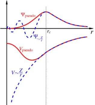
Pseudopotentials are built to reproduce the true potential of the nucleus outside the sphere of a radius rc, while inside that sphere, they are artificially smoothed as
illustrated in Figure 3.1 As a result, we deal with nicely smoothed wavefunctions.
Figure 3.1: Schematic representation of true potential V of nucleus and corresponding fast oscillating wavefunction Ψ (dashed blue line). Pseudopotential Vpseudo and
corresponding wavefunction Ψpseudo (plane red line) reproduce true potential outside
a sphere of radius rc.
The many-electrons problem is now reduced to a problem of only valence electrons. The calculations of this work have been done using the norm-conserving Hartwigsen-Goedeker-Hutter pseudopotentials [65].
3.1.5
Choice of a basis set
The choice of a basis set is crucial for the DFT calculations, as it results in accuracy and in reliability of the outputs. The basis set should meet particular
![Table 2.1: The segregation parameter k 0 for some silicon impurities and their approximate concentrations in SoG-Si [57, 132].](https://thumb-eu.123doks.com/thumbv2/123doknet/12893505.370827/18.892.250.597.113.269/table-segregation-parameter-silicon-impurities-approximate-concentrations-sog.webp)
![Figure 2.2: From reference [24].](https://thumb-eu.123doks.com/thumbv2/123doknet/12893505.370827/30.892.213.632.556.1022/figure-from-reference.webp)


![Figure 4.3 reports the Arrhenius plot of calculated diffusion coefficient together with the experimental data from Reference [60]](https://thumb-eu.123doks.com/thumbv2/123doknet/12893505.370827/60.892.167.665.701.991/figure-reports-arrhenius-calculated-diffusion-coefficient-experimental-reference.webp)
