HAL Id: lirmm-01548996
https://hal-lirmm.ccsd.cnrs.fr/lirmm-01548996
Submitted on 28 Jun 2017
HAL is a multi-disciplinary open access
archive for the deposit and dissemination of
sci-entific research documents, whether they are
pub-lished or not. The documents may come from
teaching and research institutions in France or
abroad, or from public or private research centers.
L’archive ouverte pluridisciplinaire HAL, est
destinée au dépôt et à la diffusion de documents
scientifiques de niveau recherche, publiés ou non,
émanant des établissements d’enseignement et de
recherche français ou étrangers, des laboratoires
publics ou privés.
Embedded systems to high performance computing
using STT-MRAM
Sophiane Senni, Thibaud Delobelle, Odilia Coi, Pierre-Yves Péneau, Lionel
Torres, Abdoulaye Gamatié, Pascal Benoit, Gilles Sassatelli
To cite this version:
Sophiane Senni, Thibaud Delobelle, Odilia Coi, Pierre-Yves Péneau, Lionel Torres, et al.. Embedded
systems to high performance computing using STT-MRAM. DATE: Design, Automation and Test
in Europe, Mar 2017, Lausanne, Switzerland. pp.536-541, �10.23919/DATE.2017.7927046�.
�lirmm-01548996�
Embedded Systems to High Performance
Computing using STT-MRAM
Sophiane Senni, Thibaud Delobelle, Odilia Coi, Pierre-Yves Peneau,
Lionel Torres, Abdoulaye Gamatie, Pascal Benoit, Gilles Sassatelli
University of Montpellier, LIRMM UMR CNRS 5506 Email: [email protected]
Abstract—The scaling limits of CMOS have pushed many
researchers to explore alternative technologies for beyond CMOS circuits. In addition to the increased device variability and process complexity led by the continuous decreasing size of CMOS transistors, heat dissipation effects limit the density and speed of current systems-on-chip. For beyond CMOS systems, the emerging memory technology STT-MRAM is seen as a promising alternative solution. This paper shows first how STT-MRAM can improve energy efficiency and reliability of future embedded systems. Then, a hybrid design exploration framework is presented to investigate the potential of STT-MRAM for high performance computing.
I. INTRODUCTION
Three years ago, the ITRS roadmap were reorganized ac-cording to the new challenges of semiconductor industries [1]. Among the seven focus topics of this new roadmap is “Beyond CMOS”. Indeed, several scaling issues related to the CMOS technology are observed. Decreasing the size of CMOS transistors increases significantly the static power consumption due to the high leakage current. In addition, the high density integration of CMOS components increases the amount of power per unit area. As a result, the thermal constraints oblige most of the systems to be partially switched-on while the other part is off [2]. Moreover, a stagnation of the maximum clock frequency has been observed for several years due to the heat dissipation effect, which makes difficult further improvement in performance. Although current systems implements the power-gating technique to mitigate the power consumption, this solution is constrained by a natural characteristic of CMOS-based devices: volatility. Therefore, turning off the memory part also means losing the execution state, which is not appreciated since it will require a long wake-up time to resume the execution of the application. On the other hand, leaving power to the memory system could induce a significant leakage power consumption since a large part of current systems-on-chip’s area is occupied by the memory elements.
Among the beyond CMOS solutions, several emerging memory technologies show interesting characteristics to deal with the aforementioned issues. Spin Transfer Torque Mag-netic Random Access Memory (STT-MRAM) is seen as one of the most promising by combining non-volatility, high density, low leakage and competitive access time compared to CMOS-based memories such as SRAM and Flash. The state-of-the-art showed that STT-MRAM can be included at any level of the
memory hierarchy, i.e. at main memory level, cache level, and even register level [3], [4], [5]. This paper focuses on both low-power applications and high performance computing (HPC) systems to explore the benefit of using STT-MRAM. The rest of the paper is organized as follows: Section II provides the basics of STT-MRAM technology. Section III shows the potential of STT-MRAM to design non-volatile processor with two interesting capabilities for energy-efficient and reliable embedded systems: instant-on/off and rollback. Section IV describes a hybrid design exploration flow to investigate the overall performance impact of using STT-MRAM into the memory hierarchy of HPC systems. Section V reviews related work and Section VI concludes this paper.
II. SPIN-TRANSFER-TORQUEMRAM: BASICS
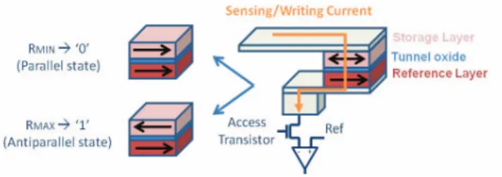
The bit cell structure of MRAM technology is depicted in Figure 1. Known as Magnetic Tunnel Junction (MTJ), it con-sists of two ferromagnetic layers separated by a thin insulating barrier. One of the two layers (reference layer) has its magnetic orientation pinned to one direction, whereas the magnetization of the other layer (storage layer) can be switched between two different directions. The information is stored as the resistance of the MTJ whose value significantly depends on the relative orientation of the two layers. The parallel state causes a low MTJ resistance and can be characterized as a logic zero. The antiparallel state provides a high MTJ resistance and can be identified as a logic one. Two kinds of magnetization of the magnetic layers can be found in STT-MRAM: in-plane and perpendicular. The former has its magnetic orientation parallel to the plan of the MTJ, whereas the latter has a magnetization perpendicular to the plan of the MTJ. Perpendicular STT-MRAM was introduced to further reduce the switching current of the MTJ and to improve scalability.
A read operation consists in sensing the state of the storage layer thanks to a current flowing through the MTJ. Regarding the write operation, the STT effect switches the magnetization of the storage layer by direct transfer of the spin angular momentum from spin-polarized electrons. The direction of the spin-polarized current through the MTJ determines the final state of the bit cell.
Regarding the last advances of the STT-MRAM technol-ogy, IBM and SAMSUNG [6] demonstrated that a specific magnetic tunnel junction stack with perpendicular magnetic anisotropy is capable of delivering good STT performance down to 10−6 Write Error Rate (WER) in a broad range of device sizes from 50nm to 11nm, on a statistically relevant sample of several hundred of devices. They demonstrated an individual 11 nm device switching down to WER =7×10⁻¹⁰ using only7.5μA.
III. STT-MRAMFOR LOW-POWER APPLICATIONS
Considering low-power applications, low-power microcon-troller units (MCUs) are proposed in the market with various low-power modes. The lowest power mode ensures the lowest power consumption during a standby state by turning off almost all components of the device. However, this mode will show the longest wake-up time to return to the active state. The volatility of CMOS involves having intermediate low-power modes to preserve the execution state by leaving power to the memory components (i.e. flip-flops, register bank, main memory). Hence, customers have to analyze the suitable low-power mode to obtain the best tradeoff between energy consumption and wake-up time, according to the application. This section shows the benefit of STT-MRAM to de-sign non-volatile processors with two interesting capabilities:
instant-on/off and rollback. The former allows a recovery of
the state of the processor after a complete shutdown. The latter gives the possibility to restore a previous valid state of the processor, for instance in the case of an execution error (soft errors) or a power failure. Both techniques are validated on two 32-bit embedded processors: Amber [7] and Secretblaze [8]. The HDL codes of both processors were modified to implement the two aforementioned capabilities. The registers retaining the state of the processor are duplicated to emulate the non-volatile STT-MRAM registers, and control logic are added to enable the backup/recovery of the system state. Considering data from the current state-of-the-art and thanks to the NVSim tool, the cost induced by implementation of the
instant-on/off and rollback techniques is finally evaluated. A. Instant-on/off
The instant-on/off function allows a processor to resume the execution of an application after a complete shutdown. It consists in saving the complete state of the processor before a power-down, then restoring the state after a new power-up. To make this possible, it is required to insert STT-MRAM at both register level and memory level. A typical flip-flop (FF) based on STT-MRAM is designed to have a dual-storage
facility (hybrid) [9]. The CMOS stage of the FF uses cross-coupled inverters (latch) to store one data bit in its electrical (volatile) form. On the other hand, the magnetic stage uses a MTJ to store one non-volatile data bit. Figure 2 illustrates a non-volatile FF architecture. In brief, assuming the FFs and the main memory of the processor are based on STT-MRAM, then the instant-on/off procedure is as in Algorithm 1:
Algorithm 1: Instant-on/off procedure
(1) For each FF, save the current state by writing the
value from the CMOS FF into the MTJ;
(2) Power down the processor. As the main memory is
non-volatile, data are preserved;
(3) Power up the processor. As the main memory is
non-volatile, data are available;
(4) For each FF, restore the backup data by reading the
value from the MTJ into the CMOS FF.
Fig. 2. MRAM-based non-volatile flip-flop architecture
The cache memory, if present, does not need to be built with STT-MRAM to enable the instant-on/off. However, per-formance penalties have to be taken into account if a volatile cache is considered. For both writing policies (i.e. write-through and write-back), a warmup period will take place after a power-up to restore data from main memory to cache memory. For the write-back policy, all cache blocks marked as “dirty” need to be written back to the main memory before a complete shutdown to preserve the state of the processor.
Thanks to STT-MRAM, the instant-on/off technique is promising to design fast and low power embedded systems. The hybrid CMOS/MTJ implementation of the FFs keeps the high performance of the CMOS during active mode, while the MTJs elements significantly reduce the leakage power during sleep mode, especially thanks to the non-volatility of STT-MRAM.
B. Rollback
The rollback technique is the ability to return to a previous valid state of the processor in the case for instance of an execution error or a power failure. This work assumes that
an error detection mechanism is available into the processor architecture to identify errors during the execution, for instance as proposed in [10]. The principle of the rollback is shown in Figure 3.
Fig. 3. Rollback principle
To avoid resetting the application of the complete system because of a soft error or a power failure, checkpoints can be created at runtime by saving the state of the processor either periodically or at strategic instant during the execution of the application. Then, if a system failure occurs, there is the possibility to come back to the last checkpoint. At register level, a checkpoint can be easily performed thanks to the dual-storage structure of the STT-MRAM FFs. At memory level, a dual-bank memory architecture is considered. One bank (main memory) is dedicated to the execution of the application whereas the other bank (checkpoint memory) is used for the backup. The size of the checkpoint memory depends on both the application and the checkpointing period. If a checkpoint (rollback) is desired, only the modified memory locations (from the last checkpoint) are backed up (restored).
In brief, assuming the aforementioned considerations, then the rollback procedure is as in Algorithm 2:
Algorithm 2: Rollback procedure
(1) Create checkpoints during the execution of the
application;
(2) A system failure is detected; (3) Stall the processor;
(4) Restore the last checkpoint consisting in;
- Restoring the state of the FFs by reading the value
from the MTJ into the CMOS FF;
- Restoring the main memory contents by copying
data from the checkpoint memory to the main memory;
(5) Resume the execution of the application.
As for instant-on/off, the cache memory does not need to be necessarily based on STT-MRAM to enable the rollback technique. In a similar way to the instant-on/off, if the cache is kept volatile, performance penalties have also to be considered (i.e. cache warmup, write back from cache to main memory). In addition, if a rollback is performed at runtime (i.e. without turning off/on the processor), the cache has to be flushed (i.e. invalidate all the cache lines) when restoring a checkpoint to avoid inconsistency between cache and memory.
Having the same low-power capability as the instant-on/off, the rollback implementation described in this section has also the potential to design more reliable devices against soft errors and power failures.
Fig. 4. Checkpoint/rollback validation
TABLE I
STT-MRAMBASED FLIP-FLOP AND MEMORY PERFORMANCES
Memory element Latency (ns) Energy (pJ) (45nm) Read Write Read Write Flip-Flop 0.2 4 0.012 0.5 Main memory (1MB) 5 14 36 52 Checkpoint memory (4kB) 1.06 10.3 8.7 34.5
C. Validation
A complete backup/recovery of the system state has been validated through register-transfer-level simulation for the Se-cretblaze and the Amber processors. A checkpoint/rollback procedure is demonstrated in Figure 4 which shows the output terminals of both processors running the DES and the blowfish cipher algorithms. In both cases, a rollback is carried out at runtime, then the application is properly re-executed from the checkpoint.
D. Cost analysis
Data from the current state-of-the-art of STT-MRAM based flip-flops (FFs) [5] are used to evaluate the overall performance cost of the instant-on/off and rollback at register level. On the other hand, the cost at memory level is quantified thanks to NVSim. Performance data of each memory element based on STT-MRAM are detailed in Table I. In this cost analysis, cache memory is not considered since it is not indispensable to enable the aforementioned techniques.
1) Register level: Among all of the FFs of the SecretBlaze,
1986 FFs contain the state of the processor, including the register file, the pipeline registers, and some other internal registers. Regarding the Amber, the state of the processor represents 1644 FFs. Considering data from Table I, each FF consumes 500fJ (12fJ) to save (restore) the state of the CMOS stage into (from) the non-volatile magnetic stage. As a result, the energy cost to backup the system comes to about1nJ for both processors, and the recovery energy comes to 24pJ and 19.7pJ respectively for the Secretblaze and the Amber.
Regarding the backup latency, it is worth noting that backing up all the FFs at the same time can lead to a high peak current, which is not appreciated for the system. Therefore, a progressive backup is considered in this work. A maximum of 500 FFs are backed up (in parallel) at a time. As 4ns is required to back up one FF, it will take 16ns to save all the FFs for both processors. This corresponds to one clock cycle latency if the system frequency is lower or equal to 62.5MHz. On the other hand, it only takes0.8ns to restore the FFs (500 FFs restored at a time,0.2ns restore time per FF).
2) Memory level: For the instant-on/off, there is no cost
related to the main memory. Since the latter is based on STT-MRAM, data are preserved before a complete shutdown of the system. For the rollback implementation, the cost to perform a
checkpoint will depends on the number of bytes it is required
to save into the checkpoint memory. In this work, the worst case is considered (i.e. the size of the checkpoint memory which is4kB). The memory architecture is implemented with a 32-bit word width. Therefore, the energy cost to backup 4kB (i.e. 1024 words) is represented by the equation 1, where
Nwords, Eread, and Ewrite are respectively the number of
words to backup, the read energy per access of the main memory and the write energy per access of the checkpoint
memory. As a result, considering the data in Table I, the
backup energy cost at memory level comes to 72.2nJ for both processors. In a similar way, the restore energy comes to 62.2nJ.
EBackup= Nwords× (Eread+ Ewrite) (1)
Regarding the latency, creating/restoring a checkpoint takes about16μs if the worst case is considered (i.e. checkpoint size of4kB).
IV. STT-MRAMEXPLORATION FORHPCSYSTEMS
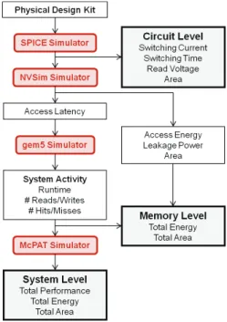
Exploring the impact of STT-MRAM on real systems requires a cross-layer investigation where device, circuit, memory, and system levels are taken into account. Such a simulation platform could be a fast and cost-effective solution to provide essential feedback to enhance the development of STT-MRAM devices. Moreover, this exploration framework would also give the possibility to evaluate hybrid designs by considering several memory technologies inside the system.
This section details first the cross-layer simulation envi-ronment (Figure 5) and the different exploration tools used to build an accurate exploration framework for performance, energy and area analysis of a full system based on STT-MRAM for HPC applications. Then, a set of results for a hybrid SRAM/STT-MRAM based L2 cache exploration is presented.
A. Hybrid design exploration framework
1) Circuit level: First of all, a Physical Design Kit (PDK) is
developed with the device-level parameters. This PDK is then used as an input for circuit-level simulation through SPICE. Thus, single bit cells and flip-flops based on STT-MRAM, sense amplifiers, and write circuits can be analyzed.
Fig. 5. Hybrid design exploration framework
2) Memory level: Memory-level evaluation is performed
thanks to NVSim [11], a performance, energy, and area estima-tor for non-volatile memories (NVM) which uses an empirical modeling methodology based on the well-known CACTI [12]. Based on circuit-level data of single bit cell (Section IV-A1) and the desired memory architecture information such as capacity, data width, and type of memory (e.g. Cache, RAM, CAM), NVSim estimates the access time, the access energy, and the total area of a complete NVM chip. This tool also includes optimization settings (e.g. buffer design optimization) and various design constraints to facilitate the design space exploration before the fabrication of the actual NVM chip.
3) System level: Memory-level information is extracted
from NVSim to explore the impact of different memory tech-nologies at system level. An accurate performance simulator (gem5 [13]) is used to simulate a single-core or a multi-core architecture with its memory hierarchy. Gem5 generates a detailed report of the system activity including the number of memory transactions (e.g. number of reads/writes, number of hits/misses) and the execution time. This activity information is then used by McPAT [14], a power and area estimator tool at architecture level. Extending the exploration framework with McPAT allows us to analyze not only the energy consumption related to the memory components, but also to evaluate the energy of the complete system including the processor cores, buses, and memory controller.
B. Hybrid L2 cache exploration
In order to get the best tradeoff between speed and power consumption, exploration of hybrid memory architecture could be done thanks to the above exploration framework. For instance, cache memories have a specific architecture based
on tag arrays and data arrays. The tag is accessed to check if the required data is present (Hit) or not (Miss) into the cache. This step has to be fast to ensure high performance. On the other hand, the data array is much larger than tag array, and need to be optimized in terms of energy consumption. As a result, a possible hybrid cache architecture is a SRAM-based tag array and a STT-MRAM data array to ensure low access time and low leakage power.
Table II shows the considered architecture for the hy-brid SRAM/STT-MRAM L2 cache exploration, including the read/write latencies (in clock cycles) got from NVSim. SRAM-only and STT-MRAM-SRAM-only based L2 caches has also been simulated for comparison purposes. The gem5 simulator has been modified to model hybrid cache architectures with dif-ferent memory technologies in tag and data arrays. Regarding the energy and area metrics, Table III details the output from NVSim for the three considered L2 caches. The study considers a45nm technology node.
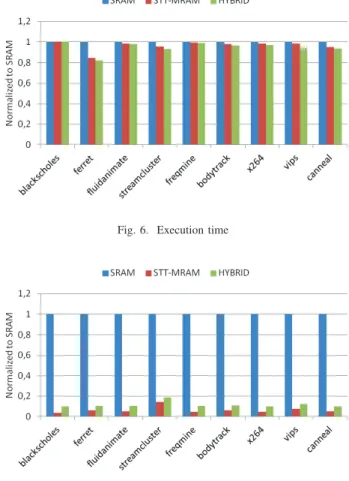
For the three different scenarios, Figures 6 and 7 re-spectively depict the execution time of the system and the energy consumption of L2 cache for different workloads of the PARSEC benchmark suite [15]. Due to its high density compared to SRAM, STT-MRAM based L2 provides a faster read access latency, which results in a smaller execution time. This fast read latency by replacing SRAM with STT-MRAM is actually noticeable only for the data array, and not for the tag array. As a result, the performance of the system is further improved for the hybrid L2 cache which considers a SRAM-based tag array and a STT-MRAM SRAM-based data array.
For the energy consumption, using a hybrid L2 cache archi-tecture results in more than 80% of gain compared to a full SRAM architecture. However, it is more energy consuming than a full STT-MRAM architecture due to the high leakage power of the SRAM-based tag array.
TABLE II
ARCHITECTURE CONFIGURATION
Hierarchy level Configuration
Processor 4-core out-of-order,1GHz, 32-bit RISC ARMv7 L1 I/D cache
Private,32kB, 4-way associative, 64B cache line SRAM (read: 2, write: 2)
L2 cache
Shared,1MB, 8-way associative 64B cache line, sequential access
SRAM (read: 11, write: 11) STT (read: 8, write: 17) HYBRID (read: 7, write: 16) Main Memory DRAM, 512MB, DDR3
TABLE III
1MB L2CACHE(ENERGY AND AREA)
Technology
Energy Cache area Read Write Leakage Total
(nJ) (nJ) (mW) (mm2)
SRAM 0.5 0.05 630 2.7
STT-MRAM 0.15 0.65 24 1.1 HYBRID 0.13 0.62 63 1.2
Fig. 6. Execution time
Fig. 7. Energy consumption of L2 cache
In order to have a better idea of the impact of the cache memories on the overall system, Figure 8 shows the energy consumption of the complete system, including the cores, L1-Instruction caches, L1-Data caches, L2 cache, buses and memory controller. As observed in the figure, the energy influence of the cache memories is small compared to that of the cores for the considered architecture. As a result, the large energy gain noticed in L2 by using STT-MRAM instead of SRAM will have a small impact on the overall system. It is worth noting that this case study considers a four-core architecture with a quite small L2 cache. In the case of fewer cores, the energy influence of the L2 cache memory on the system would be more significant.
Thanks to the exploration framework presented in this work, it is possible to explore other architecture scenarios and analyze the influence on the complete system, for instance with a different number of cores, with larger L2 cache, or with additional level of cache (e.g. L3) based on STT-MRAM. A similar analysis for the area is also possible.
V. RELATED WORK
Several works have studied possible designs of non-volatile processors thanks to MRAM, including experimental fab-rication, such as in [16], [17]. Nevertheless, the previous
Fig. 8. Energy consumption of the complete system
works only focused on the backup/recovery process within the context of a shutdown of the system. This paper also analyzed and validated the recovery of the system at runtime in the case of a rollback procedure.
Regarding the STT-MRAM based cache exploration, many studies have been carried out, such as in [18], [19]. However, in addition to the previous work, this paper presents an exploration flow which can clearly analyze the area and energy repercussions on the overall system of using STT-MRAM inside the memory hierarchy of a processor architecture.
VI. CONCLUSION
For several years, MRAM technology has been rising more and more interest to the microelectronics industry. This paper showed how this memory technology could help to design future smart devices with a great potential for energy efficiency and reliability, thanks to the instant-on/off and rollback capa-bilities. Moreover, a hybrid design exploration framework able to explore the performance impact of using STT-MRAM into the memory hierarchy of HPC systems has been presented.
Perspectives of this work is to build a real design of a hybrid system-on-chip based on STT-MRAM to strengthen the results of a possible non-volatile processor. Regarding the STT-MRAM exploration for HPC, an extension of the framework is planned to consider also STT-MRAM based main memory.
ACKNOWLEDGMENT
This work has received funding from the European Union’s Horizon 2020 research and innovation programme under grant agreement No 687973 - GREAT (heteroGeneous integRated magnetic tEchnology using multifunctional standardized sTack (MSS)), and the French National Research Agency under grants 15-CE24-0033-01 (MASTA project) and ANR-15-CE25-0007-01 (CONTINUUM project).
REFERENCES
[1] J.-A. Carballo, W.-T. J. Chan, P. A. Gargini, A. B. Kahng, and S. Nath, “Itrs 2.0: Toward a re-framing of the semiconductor technology roadmap,” in 2014 IEEE 32nd International Conference on Computer
Design (ICCD). IEEE, 2014, pp. 139–146.
[2] Z. Or-Bach, “Dark silicon – are the dark days coming?” News &
Analysis. EE Times, 2015.
[3] L. Jiang, W. Wen, D. Wang, and L. Duan, “Improving read performance of stt-mram based main memories through smash read and flexible read,” in 2016 21st Asia and South Pacific Design Automation Conference
(ASP-DAC). IEEE, 2016, pp. 31–36.
[4] K. Ikegami, H. Noguchi, C. Kamata, M. Amano, K. Abe, K. Kushida, E. Kitagawa, T. Ochiai, N. Shimomura, S. Itai et al., “Low power and high density stt-mram for embedded cache memory using advanced per-pendicular mtj integrations and asymmetric compensation techniques,” in 2014 IEEE International Electron Devices Meeting. IEEE, 2014, pp. 28–1.
[5] D. Chabi, W. Zhao, E. Deng, Y. Zhang, N. B. Romdhane, J.-O. Klein, and C. Chappert, “Ultra low power magnetic flip-flop based on check-pointing/power gating and self-enable mechanisms,” IEEE Transactions
on Circuits and Systems I: Regular Papers, vol. 61, no. 6, pp. 1755–
1765, 2014.
[6] J. J. Nowak, R. P. Robertazzi, J. Z. Sun, G. Hu, J.-H. Park, J. Lee, A. J. Annunziata, G. P. Lauer, R. Kothandaraman, E. J. OSullivan
et al., “Dependence of voltage and size on write error rates in
spin-transfer torque magnetic random-access memory,” IEEE MAGNETICS
LETTERS, vol. 7, 2016.
[7] C. Santifort, “Amber arm-compatible core,” OpenCores. org, 2010. [8] L. Barthe, L. V. Cargnini, P. Benoit, and L. Torres, “The secretblaze: A
configurable and cost-effective open-source soft-core processor,” in
Par-allel and Distributed Processing Workshops and Phd Forum (IPDPSW), 2011 IEEE International Symposium on. IEEE, 2011, pp. 310–313. [9] B. Jovanovic, R. M. Brum, and L. Torres, “Comparative analysis of
mtj/cmos hybrid cells based on tas and in-plane stt magnetic tunnel junctions,” Magnetics, IEEE Transactions on, vol. 51, no. 2, pp. 1–11, 2015.
[10] I. Wali, A. Virazel, A. Bosio, P. Girard, S. Pravossoudovitch, and M. S. Reorda, “A hybrid fault-tolerant architecture for highly reliable processing cores,” Journal of Electronic Testing, pp. 1–15, 2016. [11] X. Dong, C. Xu, Y. Xie, and N. P. Jouppi, “Nvsim: A circuit-level
performance, energy, and area model for emerging nonvolatile mem-ory,” Computer-Aided Design of Integrated Circuits and Systems, IEEE
Transactions on, vol. 31, no. 7, pp. 994–1007, 2012.
[12] N. Muralimanohar, R. Balasubramonian, and N. P. Jouppi, “Cacti 6.0: A tool to model large caches,” HP Laboratories, pp. 22–31, 2009. [13] N. Binkert, B. Beckmann, G. Black, S. K. Reinhardt, A. Saidi, A. Basu,
J. Hestness, D. R. Hower, T. Krishna, S. Sardashti et al., “The gem5 simulator,” ACM SIGARCH Computer Architecture News, vol. 39, no. 2, pp. 1–7, 2011.
[14] S. Li, J. H. Ahn, R. D. Strong, J. B. Brockman, D. M. Tullsen, and N. P. Jouppi, “Mcpat: an integrated power, area, and timing modeling frame-work for multicore and manycore architectures,” in Proceedings of the
42nd Annual IEEE/ACM International Symposium on Microarchitecture.
ACM, 2009, pp. 469–480.
[15] C. Bienia, S. Kumar, J. P. Singh, and K. Li, “The parsec benchmark suite: Characterization and architectural implications,” in Proceedings of the
17th international conference on Parallel architectures and compilation techniques. ACM, 2008, pp. 72–81.
[16] N. Sakimura, Y. Tsuji, R. Nebashi, H. Honjo, A. Morioka, K. Ishihara, K. Kinoshita, S. Fukami, S. Miura, N. Kasai et al., “10.5 a 90nm 20mhz fully nonvolatile microcontroller for standby-power-critical appli-cations,” in Solid-State Circuits Conference Digest of Technical Papers
(ISSCC), 2014 IEEE International. IEEE, 2014, pp. 184–185. [17] C. Layer, L. Becker, K. Jabeur, S. Claireux, B. Dieny, G. Prenat, G. D.
Pendina, S. Gros, P. Paoli, V. Javerliac et al., “Reducing system power consumption using check-pointing on nonvolatile embedded magnetic random access memories,” ACM Journal on Emerging Technologies in
Computing Systems (JETC), vol. 12, no. 4, p. 32, 2016.
[18] S. Takeda, H. Noguchi, K. Nomura, S. Fujita, S. Miwa, E. Arima, T. Nakada, and H. Nakamura, “Low-power cache memory with state-of-the-art stt-mram for high-performance processors,” in 2015 International
SoC Design Conference (ISOCC). IEEE, 2015, pp. 153–154. [19] R. Patel, X. Guo, Q. Guo, E. Ipek, and E. G. Friedman, “Reducing
switching latency and energy in stt-mram caches with field-assisted writing,” IEEE Transactions on Very Large Scale Integration (VLSI)
Systems, vol. 24, no. 1, pp. 129–138, 2016.


![Montage expérimental et modèle de Hecht pour la caractérisation de la collection de charge [beta] de détecteurs au silicium](data:image/gif;base64,R0lGODlhAQABAIAAAP///wAAACH5BAEAAAAALAAAAAABAAEAAAICRAEAOw==)