HAL Id: hal-01796109
https://hal.archives-ouvertes.fr/hal-01796109
Submitted on 19 May 2018
HAL is a multi-disciplinary open access
archive for the deposit and dissemination of
sci-entific research documents, whether they are
pub-lished or not. The documents may come from
teaching and research institutions in France or
abroad, or from public or private research centers.
L’archive ouverte pluridisciplinaire HAL, est
destinée au dépôt et à la diffusion de documents
scientifiques de niveau recherche, publiés ou non,
émanant des établissements d’enseignement et de
recherche français ou étrangers, des laboratoires
publics ou privés.
Curved sensors for compact high-resolution wide field
designs: prototype demonstration and optical
characterization
Bertrand Chambion, Christophe Gaschet, Thibault Behaghel, Aurélie
Vandeneynde, Stéphane Caplet, Stéphane Gétin, David Henry, Emmanuel
Hugot, Wilfried Jahn, Simona Lombardo, et al.
To cite this version:
Bertrand Chambion, Christophe Gaschet, Thibault Behaghel, Aurélie Vandeneynde, Stéphane Caplet,
et al.. Curved sensors for compact high-resolution wide field designs: prototype demonstration and
optical characterization. SPIE Photonics West 2018, Jan 2018, San Francisco, United States.
�hal-01796109�
Curved sensors for compact high-resolution wide field designs:
prototype demonstration and optical characterization
Bertrand Chambion
1, Christophe Gaschet
1, 2, Thibault Behaghel
2, Aurélie Vandeneynde
1,
Stéphane Caplet
1, Stéphane Gétin
1, David Henry
1, Emmanuel Hugot
2, Wilfried Jahn
2,
Simona Lombardo
2, Marc Ferrari
2.
1
Univ. Grenoble Alpes, CEA,
LETI, MINATEC campus, F38054 Grenoble, France.
2
Aix Marseille Univ, CNRS, LAM,
Laboratoire d'Astrophysique de Marseille, Marseille, France.
ABSTRACT
Over the recent years, a huge interest has grown for curved electronics, particularly for opto-electronics systems. Curved sensors help the correction of off-axis aberrations, such as Petzval Field Curvature, astigmatism, and bring significant optical and size benefits for imaging systems. In this paper, we first describe advantages of curved sensor and associated packaging process applied on a 1/1.8’’ format 1.3Mpx global shutter CMOS sensor (Teledyne EV76C560) into its standard ceramic package with a spherical radius of curvature Rc=65mm and 55mm. The mechanical limits of the die are discussed (Finite Element Modelling and experimental), and electro-optical performances are investigated. Then, based on the monocentric optical architecture, we proposed a new design, compact and with a high resolution, developed specifically for a curved image sensor including optical optimization, tolerances, assembly and optical tests. Finally, a functional prototype is presented through a benchmark approach and compared to an existing standard optical system with same performances and a x2.5 reduction of length. The finality of this work was a functional prototype demonstration on the CEA-LETI during Photonics West 2018 conference. All these experiments and optical results demonstrate the feasibility and high performances of systems with curved sensors.
Keywords:
Curved sensors, Detectors, Arrays, Imaging systems, Optical design, Petzval Field Curvature, High resolution, Compact, Photography, Mechanical limits, Aberrations, Field of view, Electro-optical characterization.1. INTRODUCTION
In recent years, there has been an increasing interest and demand for curved focal plane for imaging systems. By using a curved focal plane, significant size and optical benefits have been demonstrated for multiple applications, as defense, military, astronomical, consumer applications. In this paper, we propose an entire methodology and development, from curved packaging process to prototype, equipped with a curved CMOS image sensor, including mechanical and optical modeling, electro-optical characterization, opto-mechanical design, assembly and test compared to a standard optical system. This new compact architecture, specifically designed for curved sensor, providing high resolution without aspheric surfaces and demonstrate the capacity of curved sensors to reduce the complexity of any optical system.
2. CURVED SENSORS: IMPROVED ABERRATION CORRECTION
2.1 History
Bioinspired optics is an emerging field for learning the strategies from nature and leading to better solutions. In optical imagery, the most famous natural strategy is to curve the optical focal plane. In fact, all animal eyes have a curved retina, to compare with no commercial camera with curved silicon sensor. The discovery of the Petzval Field curvature by Joseph Petzval, nearly 180 years ago, shows the first human interest for curved focal plane: an object plane through lenses gives a curved image surface, depending of refractive index and diopters curvatures. This aberration is called “Petzval Field Curvature”, which can be expressed by the Petzval sum (1):
i i i i i sumn
n
r
n
n
Petzval
1 1 (1)Where n is the refractive index of the incident and refractive medium, r is the radius of curvature of the considered diopter. Usually, the correction of this aberration is done by the use of divergent elements called “field flatteners”, discovered by Charles Piazzi Smyth in 1875 [1], which minimize drastically the Petzval sum to coincide with a flat sensor. The second interest was the discovery made by Thomas Sutton in 1860, with the monocentric system, or concentric system [2]. In this system, all optical surfaces are spherical and share the same center of curvature, and with this symmetry, multiple aberrations as the coma and astigmatism are cancelled out. This is an aberration free design and will be our optical design starting point (section 3). And the third technology with an interest for sensor’s curvature was the Schmidt telescope which provide wide field of view, limited aberrations with a curved detector [4]. For all these discoveries, the use of curved sensors was possible but limited. In fact, the solid photographic plate used in the 19th centuries was too delicate for a commercial purpose. And with the patent of Hannibal Goodwin in 1887 [3], flexible photographic films have been used. Since the launch of silicon industry, image sensors has been limited to flat and rigid. But some recent developments show a new interest for curved sensors. Firstly, there are several developments on the fabrication of curved sensors. For the monolithic approach, the fabrication has been demonstrated on uncooled and cooled infrared sensors, for very compact high-performance camera [5], Charge Couple Device (CCD) [6], or Complementary Metal Oxide Semiconductor (CMOS) [7, 8]. None are in industrial production. Secondly, there are also some developments on optical improvements of optical systems with curved sensors, on optical advantages, for instance on camera-phone [9], or astronomical applications [10], and also on the simplification of optical systems by reducing weight, volume or number of lenses [11]. A study on telescope combining free-form optics and curved detectors showed also a better field of view and f number [12].
2.2 Curved packaging and process
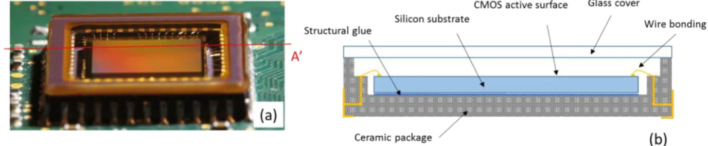
This work is based on the commercial product 1/1.8’’ format 1.3Mpx global shutter CMOS sensor (Teledyne EV76C560) [13]. The standard sensor structure basically consists of a silicon die (7.74 x 8.12 mm), glued on a ceramic package. Electrical connections are wire bonded from the die to the package surface and then, to the interconnection board thanks to a reflow process. On top, a glass cover is placed to prevent from mechanical or environment solicitations. This structure is shown in figure 1.
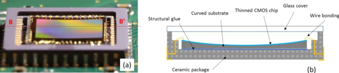
Figure 1: a) Commercial Teledyne EV76C560 flat sensor. b) Associated schematic view along A-A’ axis. In order to implement a spherically shaped CMOS sensor, changes are required to adapt this standard structure. First, the sensor is thinned with a grinding equipment to a targeted thickness in order to make the sensor mechanically “flexible”. It can be followed by a Chemical Mechanical Polishing (CMP). In this work the targeted thickness is 100µm. The bendable capabilities of the CMOS sensor will be detailed in section 2.4. Then, that thinned chip is glued (structural attachment) onto a curved substrate. The CMOS final shape is drove by the substrate. Wire bonding process, developed for electrical connections, is also optimized in order to prevent damages on thinned dies. Figure 2 shows a schematic of the final packaging, curved into its commercial packaging. The radius of curvature is R=65mm.
Figure 2: a) Curved Teledyne EV76C560 sensor (R=65mm). b) Associated schematic view along B-B’’ axis.
2.3 Associated mechanical modeling
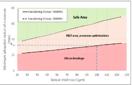
Mechanical considerations of the curved sensors are an important part to develop optical system design and find curving limitation for the sensor. For an analytical analysis, the shell theory has been used to model the mechanical behavior of the semiconductor die. This analytical model is presented in [14]. The mechanical behavior has been also modeled, using ANSYS ® Finite Element Analysis (FEA) software. For this study, extensive simulation were conducted on 7.74 x 8.12 mm (100)-oriented silicon chip with specific quadrangle elements are used, defined by 4 nodes, 6 degrees of freedom each (SHELL 181 elements). Using these elements, the principle stress values on the bottom, middle and top surfaces of the plate are obtained. Based on a breakage ball on ring study and curved packaging work [8,15] on silicon square plates with different grinding, polishing, and sawing processes, two tensile failure strength criterions has been defined: S1max1 = 200MPa, which refers to a standard grinding and sawing, and S1max2= 500MPa, associated to CMP
process and standard sawing.
The parameters are the thickness t of the plate with a range value from 25 to 125 µm and its radius of curvature. The die was discretized into approximately 5000 elements. For silicon mechanical data, the following reduced stiffness coefficient matrix is used, with only three independent elastic coefficients:
44 44 44 11 12 12 12 11 12 12 12 11 100 c c c c c c c c c c c c C (2)
where c11 = 165.7GPa, c12 = 63.9GPa, c44 = 79.6 GPa [16]. The minimum allowable radius of curvature are extracted
from the FEA results for both tensile failure strength criterions. Results of the minimum allowable radius of curvature are plotted on figure 3.
With this two failure criterions methodology, three areas are defined: the safe area without any breakage risk with a standard grinding and sawing (S1< S1max1), a forbidden area where the intrinsic silicon mechanical limits are over (S1>
S1max2), and a in between zone for processes optimizations. With our targeted thickness of 100 µm, and considering our
Figure 3: Modeling results on 7.74 x 8.12 mm (100)-oriented silicon chip in spherical shape, considering two failure criterions, S1max1 = 200MPa and S1max2= 500MPa.
According to a progressive shaping of a flat plate onto a spherical surface with a free edge boundary conditions curving process, there are two die mechanical behavior: the bi-axial tensile stress is first established in all the die for low level of radius of curvature (+inf. <Rc<60mm), and then, tangential compressive stress zones appears at the edges of the die near
the center of each of the four edges (Rc<60mm).This uniaxial compression field could be the origin of a buckling effect
as shown in a previous study on cooled IR sensor [17, 18] and due to a load-deflection response for thin-walled structures. While curving, these two behaviors are presented in figure 4a. For illustration, the tensile stress distribution (S1) of a 7.74 x 8.12 x 0.1 mm silicon plate, curved at Rc=65mm is presented in Figure 4b. For this level of curvature, all
the die is in tensile stress with a maximum bi-axial stress at the die center (201MPa) and the middle of each edges at 45MPa.
Figure 4: a) Two mechanical behaviors illustration for compression stress field generation at the middle of each edges while curving. Results of the parametric study conducted for 7.74 x 8.12 mm (100)-oriented silicon chip in spherical
shape Rc=65mm. Note that all the in plane stress is tensile, even the middle of each die edges.
2.4 Experimental assessment
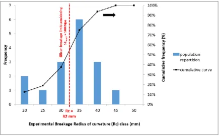
In order to validate our simulation model accuracy, bendable capability tests have been conducted on 16 representative (100) bulk silicon samples, thinned at 100µm. The experimental setup is based on a 3D printed spherical molds (Rc from 90 to 20 mm with 5 mm steps), made up of two parts, one convex, concave for the other. The sample is
placed in-between these 2-part mold and a 0.8 bar pressure is applied to force the shaping of the sample. The results is binary: breakage or not breakage of the sample. The results are summarized in Figure 5 and compared to simulated limits presented before in section 2.3 assuming S1max2. Considering an 80% cumulative frequency, a minimum allowable radius
of curvature is experimentally found at Rc min = 35 mm.
Figure 5: Experimental bendable capabilities conducted on 7.74 x 8.12 x 0.1 mm (100)-oriented silicon chip in spherical shape and associated tensile stress limit at S1max2= 500MPa. This study shows a minimum allowable radius of
curvature at Rc min = 35 mm (80% of cumulative frequency).
We first show a good accordance between measured (Rcmin, exp= 35 mm) and model results (Rcmin, model= 32 mm). It
illustrates that our FEM model gives a good prediction of the strains for silicon dies. Then, some sample broke below the simulated limit. It could be explained by a non-perfect shaping of the samples in the mold during experimental test. Another explanation could be the ultimate tensile strength value considered in the model. GENTER [8] has shown that for silicon plate, and for spherical shaping, the maximum ultimate tensile stress could be over 500MPa before breakage.
2.5 Electro-optical response
An important point to address is the curvature influence on the sensor functionality. Due to tensile or compressive stresses applied on the CMOS active layers, the electro-optical response of the CMOS stack could be modified. One of the most important parameter is the dark current: The dark current is the slope of the dark signal as a function of the integration time, in obscurity. Commercial flat sensors and curved one (Rc = 65mm) have been tested. For commercial
sensors, and stabilized à 25°C, we recorded a dark current at 450 electrons per second (e-/s). We did the same for curved
samples and a 458 e-/s is found. Dark noise (e-) and coefficient conversion (DN/e-) have been also measured. Values are
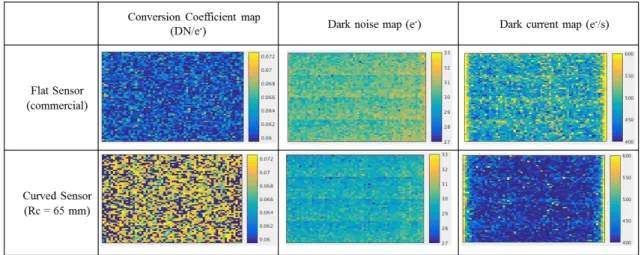
summarized in table 1. Results on curved sensor show a standard response compared to flat sensor. In order to quantify the stress map onto the sensor response, dark current, noise, and conversion coefficient maps are plotted in table 2 for flat sensor and for curved sensor at Rc=65 mm. for each map, we calculated average values every 20x16 pixels clusters.
No stresses maps signatures are visible. With all of these measurements, we can confirm that within (+inf.; 55mm) radius of curvature range, curving process has no significant impact on the Teledyne EV76C560 chip electro-optical response.
Measured on commercial sensor Curved sensor at Rc =65mm Difference Conversion Coefficient (DN/e-) 0.062 0.072 +16% Dark noise (e-) 30.4 29.6 +3% Dark current (e-/s) 493 416 -16%
Table 1: Experimental tests on electro-optical response of flat and curved Teledyne EV76C560 CMOS image sensor at 25°C (considering +7.5%.°C-1 for dark current).
Table 2: Response maps comparison on dark current, noise, and conversion coefficient. Average values every 20x16 pixels clusters. (Dark current values are extrapolated to 25°C considering +7.5%.°C-1).
3. PROTOTYPE CAMERA DESIGN DEVELOPEMENT
3.1 Monocentric lens optimization
In this part, the objective is to obtain an innovative simpler architecture specifically adapted to the curved technology. As presented in section 2.1, one architecture with curved sensor already exists: the monocentric system. This system combines compactness, wide Field of View (more than 120°), high resolution and large light collection [11]. But the technical problem of this monocentric system is the highly curved focal plane. For example, in order to address an 80° FOV with a 2 glasses monocentric system, a sensor with a size of 15.4 mm and with a radius of curvature of 12 mm is required. According to mechanical limits presented 2.3, it is impossible to curve so much the sensor without breaking it, even if it is thinned down to 10 microns. We have studied modifications on this monocentric system to provide an optical system in accordance with the sensor mechanical limits. One possibility in order to have a feasible system is described as follows. Light emerging from the monocentric system can have a large chief ray angle when the system has a wide field of view. This large angle can be problem in order to have a less curved sensor. By placing convergent lenses after the monocentric block, we can control this angle, as we can see in the figure 6a. Divergent lenses (figure 6b) are placed after convergent lenses in order to correct aberrations like the Petzval field curvature of the system and also those added by convergent lenses and the loss of the optical symmetry.
Figure 6: a) Control of the exiting light angle from the monocentric block with a convergent lens. b) Control of aberrations with a divergent lens.
The loss of symmetry interacts with monocentric block and also the aperture position. For the aperture position, one of the best positions is in front of the lens (figure 7). In fact, placing the aperture stop after convergent lenses can reduce the field of view of the system. And the monocentric block is no longer symmetric, becoming just a convergent lens. In this way, we founded a new optical design based on this architecture. The first-order proprieties of this new optical architecture are as follow. We considered different designs with a focal length between 8 and 16mm, with a corresponding sensor format between 1/2”and 2/3”. With these sensor’s formats, we obtain a large Field of View (FOV), between 40° and 50°, for these equivalent focal lengths, around 50-60mm. These sensors are thinned down to 100 μm
and curved at a radius of curvature between 50 and 86 mm compatible with the safe area presented in section 2.3. This new architecture provides a great compactness and a high resolution for a design without aspheric surfaces: 24 mm in axial length from stop aperture to the sensor. This architecture is made for low cost applications, when high resolution and compactness are needed.
Figure 7: Schematic representation of CEA-Leti unsymmetrical monocentric based optical system equipped with a spherically curved image sensor.
3.2 Final optical system performances
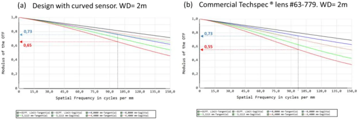
We specifically optimized a system with 12 mm focal length, a 1/1.8” sensor bended at -65mm, a 2.6 f/# and a FOV of 42°. In order to characterize optical performances of this optical system, the polychromatic Modulation Transfer Function (MTF) was calculated in Zemax lens design software for different fields and compared to an equivalent commercial design (Techspec® high resolution fixed focal length lens #63-779) with a flat sensor Teledyne EV76C560 with the same focal, field of view, resolution, and Working Distance (WD) of 2 meters.
As the final objective of the optical study is to show an important optical system size reduction of an existing one, our design shows at 0° field a very good performance with an MTF of about 73% at 100 cycles/mm, as commercial one performance. For the maximal field, the MTF is over 65% at 100 cycles/mm, compared to 55% for the commercial one. It shows that curved technology helps optical design to enhance image quality over the field. Optical performances comparisons (MTF) are plotted in figure 8.
Figure 8: a) Simulated MTF of the CEA LETI Optical design. b) Simulated MTF of Techspec® lens #63-779.
4. PROTOTYPE DEMONSTRATION
4.1 Mechanical mounting
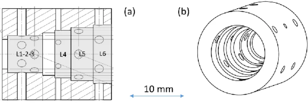
Opto-mechanical design is a key step in optical system development. It has to be easy to mount and align lenses, with high precision machining, within optical tolerances. As our prototype is a fixed focal system, we choose to design a 1-part cylindrical mechanical holder with increasing diameter values along the optical axis to align and glue each lens,
from L1 to L6. Several radial holes are drilled for each optical block to make the gluing step easier with standard optical glues. The material used is aluminum and the internal mechanical tolerance on diameters is +- 5µm. Drawings are presented in figure 10.
Figure 10: Schematic views of our opto-mechanical holder. a) Cross section. b) 3D view.
4.2 Prototype specifications and comparison to existing system
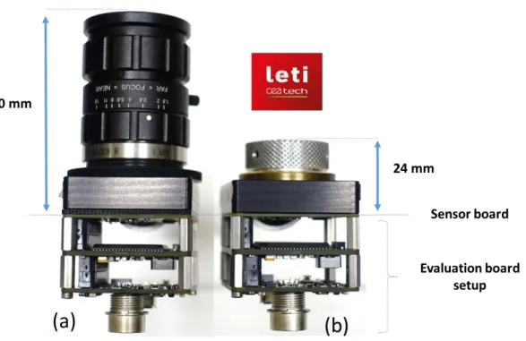
The final prototype is built on the commercial 1/1.8” format Teledyne EV76C560 CMOS image sensor evaluation kit. Basically, the standard flat sensor has been replaced by a curved-one, packaged as described in section 2.2. The radius of curvature of the sensor is R=65 mm and the opto-mechanical part is aligned and linked to the sensor thanks to a standard plug.
In order to make a performance comparison to an existing system, a Techspec® high resolution fixed focal length lens #63-779 commercial optical system has been mounted on the same evaluation kit with flat sensor. In figure 11, systems comparison views are proposed to highlight the high level of simplification we can reach by using a curved sensor. The main gain is the length reduction. Both design are the same optical performances (describes in figure 9), but the use of curved sensor allow to drastically simplify the optical part and bring technical advantages:
Reduction of the total length of the system (x2.5) Saving lenses (40%)
Make the system easier to assemble (less lenses to align) All of the optical and physical specifications are summarized in table 3.
Figure 11: Optical system comparison: a) commercial system and b) CEA-Leti equivalent performances prototype equipped with curved sensor. Curved sensor leads a x2.5 total length reduction.
Table 3: Optical and physical characteristics comparison between commercial design and CEA-Leti Design with curved sensor.
4.3 Preliminary optical tests
In order to characterize the optical performances, images from both systems have been captured and data analysis is in progress to extract and compared optical key parameters such as MTF or relative illumination. Also, a demonstration mockup has been presented on CEA-LETI booth during Photonics West 2018 conference to demonstrate the huge interest of curved technology for imaging systems.
5. CONCLUSION
Curved sensor technology is a disruptive approach for a number of scientific fields including photography, videography, computer vision and automation, surveillance imaging, microscopes, and telescopes, among others. Using a curved sensor can improve performances: considering equivalent optical performances, curved technology can reduce the system size, remove lenses, and reduce cost and complexity of an existing system. In this paper, a fully functional prototype of optical design using curved sensor is presented with a detailed following methodology: curved packaging technology with a free edge bending process and sensor mechanical limits investigation, curved sensor integration in
standard package, electro-optical characterization, and optical design using Zemax ® tool, opto mechanical design with lenses integration and optical performances comparison to an existing commercial design. Using our free edge bending process, we have created a prototypes of curved 1/1.8” format CMOS sensor bended at Rc=65mm and 55mm into its
standard package, without any electro-optical response modifications. This process is compatible with any sensor size and large scale manufacturing processes. On a f/2.6 12 mm focal length system with a 1/1.8” format sensor (Teledyne EV76C560), using our curved technology, we demonstrate an impressive simplification of the optical system (-40% of lenses) and a huge reduction of the total length by 2.5 time for the same optical performances. The finality of this work was a functional prototype demonstration on the CEA-LETI booth during Photonics West 2018 conference.
6. AKNOWEDGMENTS
This activity was partially funded by the French Research Agency (ANR) under the LabEx FOCUS ANR-11-LABX-0013, and the European Research Council through the H2020-ERC-STG-2015–678777 ICARUS program.
7. REFERENCES
[1] Ray, S. F., [Applied Photographic Optics], Third Edition, Focal Press, pp 255-256 (2002). [2] Sutton, T., «Panoramic Photography," J. of the Photographic society 95, p 185 (1860). [3] Goodwin, H., "Photographic pellicle and process of producing same," "US 610861", (1898).
[4] Lemaitre, G. R. , [Astronomical Optics and Elasticity Theory: Active Optics Methods,] Astronomy and Astrophysics Library (Berlin: Springer), pp 221 (2009).
[5] Dumas, D. , M. Fendler, N Baier, J. Primot, and E. Le Coarer, "Curved focal plane detector array for wide field cameras," Applied Optics 51, no. 22, pp. 5419-5424 (2012).
[6] Andanta, "CCD product datasheet", http://www.andanta.de/.
[7] Itonaga, K. , et al "A Novel Curved CMOS Image Sensor Integrated with Imaging System", Sony R&D Platform, Atsugi, Japan. Symposium on VLSI Technology (2014).
[8] Guenter, B. , et al., "Highly Curved Image Sensors: A Practical Approach for Improved Optical Performance," Optics Express 25, no. 12 (2017).
[9] Reshidko, D., and Jose Sasian, "Optical Analysis of Miniature Lenses with Curved Imaging Surfaces," Applied Optics 54, (2015).
[10] Hugot, E., et al "Flexible focal plane arrays for UVOIR wide field instrumentation," Proc. SPIE 9915, High Energy, Optical, and Infrared Detectors for Astronomy VII, (2016).
[11] Stamenov, I. , Ilya P. Agurok, and Joseph E. Ford, "Optimization of Two-Glass Monocentric Lenses for Compact Panoramic Imagers: General Aberration Analysis and Specific Designs," Applied Optics 51, (2012)
[12] Muslimov, E. et al., "Combining Freeform Optics and Curved Detectors for Wide Field Imaging: A Polynomial Approach over Squared Aperture," Optics Express 25, (2017).
[13] Specification sheet of Teledyne (E2V)EV76C560: https://www.e2v.com/products/imaging/cmos-image-sensors/ev76c560/
[14] Timoshenko, S. and Woinowsky-Krieger, S., Theory of Plates and Shells, 2nd edition, McGraw-Hill, 1963. [15] Zhao, J.-H., et al., Experimental evaluations of the strength of silicon die by 3-point-bend versus ball-on-ring tests,
IEEE Trans. Electron. Packag. Manuf., vol.32(4), pp.248–255 (2009).
[16]Mason, W. P. Physical Acoustics and the Properties of Solids. Princeton: Van Nostrand. (1958).
[17] Chambion, B., et al “Tunable curvature of large visible CMOS image sensors : Towards new optical functions and system miniaturization”, Proc. 66th ECTC, Las Vegas, 2016.
[18]Tekaya, K. et al, “Mechanical behavior of flexible silicon devices curved in spherical configurations,” in 2013 14th International Conference on Thermal, Mechanical and Multi- Physics Simulation and Experiments in