HAL Id: hal-02952041
https://hal.archives-ouvertes.fr/hal-02952041
Submitted on 18 Nov 2020
HAL is a multi-disciplinary open access
archive for the deposit and dissemination of
sci-entific research documents, whether they are
pub-lished or not. The documents may come from
teaching and research institutions in France or
abroad, or from public or private research centers.
L’archive ouverte pluridisciplinaire HAL, est
destinée au dépôt et à la diffusion de documents
scientifiques de niveau recherche, publiés ou non,
émanant des établissements d’enseignement et de
recherche français ou étrangers, des laboratoires
publics ou privés.
Tunable Mie-resonant dielectric metasurfaces based on
VO2 phase-change materials
Sergey Kruk, Jimmy John, Zhen Zhang, Hai Son Nguyen, Lotfi Berguiga,
Pedro Rojo Romeo, Regis Orobtchouk, Shriram Ramanathan, Yuri Kivshar,
Sébastien Cueff
To cite this version:
Sergey Kruk, Jimmy John, Zhen Zhang, Hai Son Nguyen, Lotfi Berguiga, et al.. Tunable Mie-resonant
dielectric metasurfaces based on VO2 phase-change materials. CLEO: QELS_Fundamental Science,
May 2020, Washington, United States. pp.FTh3Q.4, �10.1364/CLEO_QELS.2020.FTh3Q.4�.
�hal-02952041�
Tunable Mie-resonant dielectric metasurfaces
based on VO
2
phase-change materials
Sergey Kruk1, Jimmy John2, Zhen Zhang3, Hai Son Nguyen2, Lotfi Berguiga2, Pedro Rojo Romeo2,
Régis Orobtchouk2, Shriram Ramanathan3, Yuri Kivshar1 and Sébastien Cueff2 1Nonlinear Physics Centre, Research School of Physics, Australian National University, Canberra ACT 2601, Australia 2 Institut des Nanotechnologies de Lyon, INL-CNRS/UMR5270, Ecole Centrale de Lyon, FR 69134 Ecully Cedex, France.
3School of Materials Engineering, Purdue University, West Lafayette, IN 47907, USA
Author e-mail address: [email protected]
Abstract: We demonstrate Mie-resonant silicon metasurfaces tunable via the insulator-to-metal
transition of a deposited VO2 layer. We observe two orders of magnitude modulation depth of the metasurface reflection with reversible properties and a hysteresis-like behavior.
OCIS codes: (160.4236) Nanomaterials; (310.6628) Subwavelength structures, nanostructures; (220.4241) Nanostructure fabrication
1. Introduction
Metasurfaces have emerged as a flexible and efficient platform for manipulating electromagnetic waves. Although there has been a considerable progress in the development of plasmonic metasurfaces, some of their functionalities remain compromised by Ohmic losses and heating. More recent developments suggest an alternative way towards highly efficient metasurfaces based on Mie-resonant nanostructures made of high-index dielectric materials [1].
While static all-dielectric resonant metaphotonics is reaching maturity, big challenges remain in the design and fabrication of efficient reconfigurable and tunable structures [2] that are highly desirable for a number of applications in optical communications, information storage, imaging, detectors, and sensors. A promising pathway towards tunable metasurfaces is an incorporation of phase-change materials into the design. While substantial efforts have been made towards tunable nanophotonic devices made of metallic nanostructures coupled to various phase-change materials such as GeSbTe, VO2, etc. [2-4], all-dielectric tunable nanostructures remain largely unexplored.
In particular, VO2 is an attractive phase-change material [5] and its tunability occurs at temperatures close to ambient (~68°C). The transition can be triggered thermally, optically, or electrically. Furthermore, the dynamical change of phase corresponds to a crystalline–to–crystalline transition and therefore not accompanied by catastrophic volume change, void creation, etc, enabling a hybrid integration of this material into complex nanostructures. Therefore, VO2 is compatible with materials and/or technologies that cannot support thigh temperatures and high energy pulses needed to switch back and forth other phase-change materials such as GST. Nanofabrication of VO2 remains largely premature, and its hybrid integration with dielectric nanophotonics imposes significant challenges.
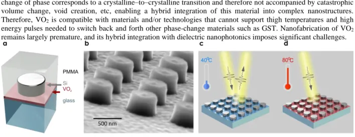
Fig. 1. (a) Design concept: a silicon meta-atom is embedded into glass/PMMA surrounding with a buried thin VO2 layer. VO2 thickness: 25 nm,
Si disk height: 240 nm, disk radius: 270 nm, square lattice period: 800 nm, PMMA layer thickness: 400 nm. (b) Electron microscope image of the fabricated Si-VO2 metasurface prior to the PMMA coating. (c-d) Functionality concept: (c) at low temperatures, the metasurface reflects light at a
designed wavelength, and (d) at high temperature the light is absorbed by the metasurface.
Here we design, fabricate, and characterize a dielectric metasurface made of Si resonators coupled to a layer of VO2 phase-change material, as presented in Figs. 1(a, b). The metasurface is designed to support both electric and magnetic Mie modes. The phase state of the VO2 layer defines the interaction between an incident light and two resonant modes. Reversible tuning of VO2 allows to approach a regime of coherent perfect absorption reducing metasurface reflection by more than two orders of magnitude (see a sketch in Figs. 1(c, d). We perform numerical calculations of the metasurface in CST Microwave Studio with the parameters specified in the caption to Fig. 1.
2. Demonstration of reversible tuning of silicon metasurfaces via VO2 phase change
To fabricate the metasurface, we start with a 25 nm thin VO2 layer deposited on quartz by magnetron sputtering from a V2O5 target under Ar/O2 partial pressure. During the deposition, the substrate temperature is maintained at 750°C to crystallize the VO2 layer during growth. We then deposit a 240 nm-thick layer of amorphous Silicon (a-Si) by plasma-enhanced chemical vapor deposition using SiH4 precursor at a temperature of 300°C. Hydrogen Silsesquioxane (HSQ) resist is then spun on the sample and patterned using E-beam lithography. After development in TMAH, the HSQ resist is used as a hard mask to transfer the patterns into a-Si via ICP-RIE dry etching with Cl2/Ar. Finally, a 400-nm-thick layer of PMMA is spun on the sample. A small part of the sample is covered by a 200-nm-thick gold serving as a reference layer for the reflection measurements.
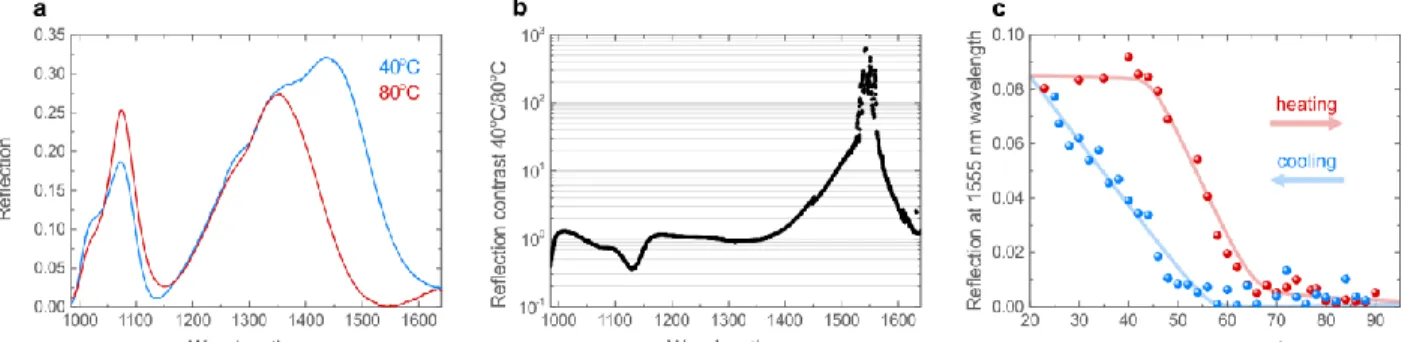
To measure optical properties and VO2-induced tunability of the metasurface, the sample is placed on a heat cell enabling ± 0.1°C temperature control. A broadband light source (halogen lamp) is focused on the devices through a 10x objective and the reflection from the metasurface is collected with the same objective. Reflected light is then dispersed in a spectrometer and detected with an InGaAs IR camera. The setup response is calibrated using a gold reference layer deposited on the sample. To measure the reversible tunability, the temperature is raised from 23°C to 90°C and back to room temperature. The heating-cooling cycle is repeated 10 times with no noticeable changes to the sample performance. A spectrum is collected every 2°C. In Fig. 2(a), we show two reflection spectra corresponding to insulator (40oC) and metal (80oC) phases of VO2 layer. Fig. 2(b) emphasizes the experimentally observed reflection contrast between the two states. At a wavelength 1550 nm that corresponds to the fiber communication C-band, the modulation depth exceeds two orders of magnitude. Finally, in Fig. 2(c) we trace the reflection at 1550 nm and observe a hysteresis behavior of reflection versus temperature. In the region 30oC—70oC the metasurface reflection can be in one of the two states depending on the history of heating-cooling cycles.
Fig. 2. Experimental results on the tunable reflection of the Si-VO2 metasurface. (a) Reflection spectra for two temperature points: 40oC (a
dielectric phase of VO2) and 80oC (a metallic phase of VO2). (b) Reflection contrast between the two temperature points. (c) Reversible
temperature tuning of the metasurface reflection at 1550 nm wavelength exhibiting a hysteresis-like behavior.
3. Conclusions and outlook
We have demonstrated, for the first time to our knowledge, the Mie-resonant silicon metasurfaces tunable by VO2. The reversible tuning of the VO2 state introduces two-orders-of-magnitude modulation depth in the metasurface reflection. The metasurface optical response further features a hysteresis behavior thus possessing a non-volatile memory of its state. We believe our work uncovers a great potential of tunable dielectric metasurfaces for manipulating light in a rapid manner as the phase transition can be driven by fast light pulses. It paves the way to nanoscale optical switches, modulators, and sensors based on all-dielectric resonant metasurfaces.
4. Acknowledgements
The authors acknowledge a financial support from the Australian National University Strategic Fund and from the French National Research Agency (ANR) under the project SNAPSHOT (ANR-16-CE24-0004). We acknowledge the support of the International Associated Laboratory in Photonics between France and Australia (LIA ALPhFA).
5. References
[1] S. Kruk and Y. Kivshar, “Functional meta-optics and nanophotonics governed by Mie resonances”, ACS Photonics 4, 2638 (2017).
[2] M. Wuttig, H. Bhaskaran and T. Taubner, “Phase-change materials for non-volatile photonic applications”, Nature Photonics 11, 465 (2017). [3] S. Cueff, D. Li, Y. Zhou, F.J. Wong, J.A. Kurvits, S. Ramanathan, and R. Zia. “Dynamic control of light emission faster than the lifetime limit
using VO2 phase-change”, Nature Communications 6, 8636 (2015).
[4] Y. Kim, P.C. Wu, R. Sokhoyan, K. Mauser, R. Glaudell, G. K. Shirmanesh, and H.A. Atwater, “Phase modulation with electrically tunable
vanadium dioxide phase-change metasurfaces” Nano Letters 19, 3961−3968 (2019).