Publisher’s version / Version de l'éditeur:
Vous avez des questions? Nous pouvons vous aider. Pour communiquer directement avec un auteur, consultez la première page de la revue dans laquelle son article a été publié afin de trouver ses coordonnées. Si vous n’arrivez pas à les repérer, communiquez avec nous à [email protected].
Questions? Contact the NRC Publications Archive team at
[email protected]. If you wish to email the authors directly, please see the first page of the publication for their contact information.
https://publications-cnrc.canada.ca/fra/droits
L’accès à ce site Web et l’utilisation de son contenu sont assujettis aux conditions présentées dans le site LISEZ CES CONDITIONS ATTENTIVEMENT AVANT D’UTILISER CE SITE WEB.
Optics Express, 28, 25, pp. 37971-37985, 2020
READ THESE TERMS AND CONDITIONS CAREFULLY BEFORE USING THIS WEBSITE.
https://nrc-publications.canada.ca/eng/copyright
NRC Publications Archive Record / Notice des Archives des publications du CNRC :
https://nrc-publications.canada.ca/eng/view/object/?id=0c804ef0-058b-4363-99e5-1f95af3dc617
https://publications-cnrc.canada.ca/fra/voir/objet/?id=0c804ef0-058b-4363-99e5-1f95af3dc617
This publication could be one of several versions: author’s original, accepted manuscript or the publisher’s version. / La version de cette publication peut être l’une des suivantes : la version prépublication de l’auteur, la version acceptée du manuscrit ou la version de l’éditeur.For the publisher’s version, please access the DOI link below./ Pour consulter la version de l’éditeur, utilisez le lien DOI ci-dessous.
https://doi.org/10.1364/OE.404364
Access and use of this website and the material on it are subject to the Terms and Conditions set forth at
Narrowband Bragg filters based on subwavelength grating waveguides
for silicon photonic sensing
Pérez-Armenta, Carlos; Ortega-Moñux, Alejandro; Čtyroký, Jiří; Cheben,
Pavel; Schmid, Jens H.; Halir, Robert; Molina-Fernández, Íñigo;
Narrowband Bragg filters based on
subwavelength grating waveguides for silicon
photonic sensing
C
ARLOSP
ÉREZ-A
RMENTA,
1,*A
LEJANDROO
RTEGA-M
OÑUX,
1J
I ˇR͡
C
TYROKÝ,
2P
AVELC
HEBEN,
3J
ENSH. S
CHMID,
3R
OBERTH
ALIR,
1,4Í
ÑIGOM
OLINA-F
ERNÁNDEZ,
1,4 ANDJ. G
ONZALOW
ANGÜEMERT-P
ÉREZ11Universidad de Málaga, Dpto. de Ingeniería de Comunicaciones, ETSI Telecomunicación, 29071 Málaga,
Spain
2CAS Institute of Photonics and Electronics, CAS, Chaberská 57, 182 51 Prague, Czech Republic 3National Research Council Canada, Ottawa, Ontario K1A 0R6, Canada
4Bionand Center for Nanomedicine and Biotechnology, Parque Tecnológico de Andalucía, Málaga 29590,
Spain
Abstract: Subwavelength grating (SWG) waveguides have been shown to provide enhanced light-matter interaction resulting in superior sensitivity in integrated photonics sensors. Narrowband integrated optical filters can be made by combining SWG waveguides with evanescently coupled Bragg gratings. In this paper, we assess the sensing capabilities of this novel filtering component with rigorous electromagnetic simulations. Our design is optimized for an operating wavelength of 1310 nm to benefit from lower water absorption and achieve narrower bandwidths than at the conventional wavelength of 1550 nm. Results show that the sensor achieves a sensitivity of 507 nm/RIU and a quality factor of 4.9 × 10⁴, over a large dynamic range circumventing the free spectral range limit of conventional devices. Furthermore, the intrinsic limit of detection, 5.1 × 10⁻⁵RIU constitutes a 10-fold enhancement compared to state-of-the-art resonant waveguide sensors.
© 2020 Optical Society of America under the terms of theOSA Open Access Publishing Agreement
1. Introduction
Silicon photonics is a key technology for the optical communication systems as well as a promising platform for chemical and biochemical detection [1,2]. The latter is important for many applications, including medical diagnosis, food safety controls, environmental monitoring and biological and chemical research and development. In addition to the good sensitivity achieved by silicon-based devices, the main advantages of using this platform are the small footprint and the compatibility with CMOS manufacturing processes, which facilitates the fabrication at low cost and the integration in lab-on-a-chip systems.
Most photonic integrated sensors are based on evanescent field sensing. They exploit the interaction between the evanescent field of a guided mode and the surrounding medium to detect changes in the effective index of the mode due to changes of the external refractive index. The changes in the effective index of a waveguide mode is typically mapped to a quantity that can be readily detected. For example, interferometric sensors map the change in the effective index into an intensity variation [3,4], while resonant sensors convert it into wavelength shifts [5,6]. Therefore, the capabilities offered by different photonic sensors, like their sensitivity and limit of detection, strongly depend on both the sensing waveguide and the sensing architecture used in the detection process [7,8].
#404364 https://doi.org/10.1364/OE.404364
Regarding the sensing waveguides, different types of waveguide geometries have been proposed in the literature. Initially, conventional photonic wires were used [9]. However, a significant fraction of the electric field is confined in the core of the waveguide for TE modes or is present in the buried oxide layer for TM modes, thereby leading to resonant sensors with modest values of device bulk sensitivity between 70 nm/RIU and 200 nm/RIU for TE and TM polarization [6,10], respectively. Alternative solutions with stronger light-matter interactions have subsequently been explored. These include the slot waveguide, with a sensitivity of 300 nm/RIU [5] and the subwavelength grating (SWG) waveguide with sensitivities over 400 nm/RIU [11–14] and intrinsic Limits of Detection (iLoD) near 5 × 10⁻⁴RIU. More recently, SWG-slot waveguides [15] with a bulk sensitivity of 599 nm/RIU or the SWG-multibox waveguides [16,17], with sensitivities of up to 579 nm/RIU and iLoDs of 10−4−10−3have been reported.
Focusing on SWG waveguides, their potential for sensing arises from their capability to modify the spatial distribution of the mode profile, thereby maximizing the light-matter interaction, as shown for the first time in [18]. However, SWG based sensors still have room for further improvements. For instance, SWG sensing waveguides have mainly been used in ring-resonator based architectures [11–14], and more recently for bimodal waveguides [19] with bulk sensitivities as large as 2270 nm/RIU. The dimensions of the SWG waveguides tipically used in evanescent field sensors have not been specifically optimized for sensing application, inheriting parameters from other (tipically telecom) applications (i.e., 220 nm thick and 400–600 nm wide silicon wire waveguides). A recent study at 1550 nm for TE polarization has demonstrated that a further enhancement of the light-matter interaction is achievable by thickening and narrowing the silicon segments of SWG waveguides [7]. Finally, the operating wavelength has typically been 1550 nm. This is an issue when the deposited fluid in the sensor is water-based, since water absorption at 1550 nm is larger compared to shorter wavelengths, e.g., 1310 nm telecom band (52.5 dB/cm and
6.6 dB/cm, respectively) [1,8,20].
SWG waveguides are of great interest not only for sensing applications, but for silicon photonics in general [21]. For example, recently an ultra-narrowband Bragg-type filter which achieves measured bandwidths as narrow as 150 pm, yet maintains minimum structural features as large as 100 nm [22,23], has been demonstrated. This device, represented in Fig.1, comprises two arrays of periodic loading silicon blocks operating in the Bragg regime which are evanescently coupled to a central SWG waveguide operating in the subwavelength regime. By controlling the separation distance between the Bragg loading segments and the SWG waveguide core, the bandwidth can be adjusted by design over a broad range.
Fig. 1. Top and perspective view of the Bragg filter structure proposed in [22] and experimentally demonstrated in [23] that has been analyzed as a sensor in this paper.
In this work we propose the use of such a Bragg-type filter as a sensing structure and optimize its performance. Small bandwidths can be achieved with this approach resulting in a low iLoD. Furthermore, the Bragg filter sensor exhibits a virtually unlimited free spectral range, thus
overcoming the inherent ambiguity of both interferometric and ring resonator architectures with a periodic response to the measured signal. Our Bragg grating sensor is thus able to detect a large range of refractive index values, breaking existing trade-offs between sensitivity and dynamic range. Optimization of the SWG geometry for operation at a wavelength of 1310 nm, where water absorption is much lower than at 1550 nm, yields a reduction of the iLoD of around one order of magnitude. The simulation results show that the proposed architecture achieves a bulk sensitivity of 507 nm/RIU, a quality factor of 4.9 × 10⁴and a remarkably high iLoD of 5.1 × 10⁻⁵ RIU, which constitutes a 10-fold reduction compared to other state-of-the-art resonant sensors. The paper is organized as follows. In section2, the geometry of the structure is presented along with the models which have been used to study and simulate our device. In section3, the fundamental metrics for Bragg refractive index sensors are introduced and our design approach is discussed in more details. In section4the key findings of this work are summarized and conclusions are drawn.
2. Narrowband SWG Bragg filters: geometry, modeling and general considera-tions
2.1. Sensor geometry
The SWG based Bragg filter schematic is shown in Fig.1. It exhibits a double periodicity, namely the period ΛSWGin the central SWG waveguide and the period ΛBof the array of lateral loading blocks separated from the central SWG waveguide by a distance s. The loading blocks are designed to make the structure operate in the Bragg regime at the operational wavelength, so that at Bragg resonance the forward propagating mode is reflected backwards.
According to the perturbation theory [24], we consider the central SWG waveguide core as the unperturbed structure and the lateral loading blocks as the perturbation. The width (w), height (h), pitch (ΛSWG)and duty cycle (DC = a/ΛSWG)[see Fig.1] of the unperturbed waveguide are primarily chosen to maximize the light-matter interaction. Its effective index (neff,u)and the pitch also must ensure that the waveguide is operating in the SWG regime at the wavelength of interest (neff,u<λ/2ΛSWG)[25]. To minimize substrate leakage loss, the criterion neff,u>1.65 or neff,u>1.55 is used, depending on the thickness of Buried Oxide (BOX), 2 µm or 3 µm, respectively [26]. Furthermore, once the loading blocks are introduced, ΛB and the effective index of the full structure must fulfill the Bragg condition
neff= λr
2ΛB (1)
at the desired Bragg wavelength λr. The spectral bandwidth will depend on both the block size (t × u × h)and the distance s at which they are placed: the more separated from the core or the smaller the blocks are, the narrower is the bandwidth. Note that the perturbation model used in this work will be valid as long as the perturbation is weak, i.e. when s is large enough (500 nm or more). In that case, introducing the blocks will not appreciably change the mode effective index (neff ≈ neff,u).
The device is designed for the Silicon-on-Insulator (SOI) platform, with a buried oxide thickness
hBOX. The analyte is assumed to be water-based, effectively acting as the upper waveguide
cladding layer. Any change in the analyte refractive index ncwill lead to a corresponding change in the resonance wavelength of the filter λr.
2.2. Coupled mode theory
Coupled Mode Theory (CMT) [24] has been successfully applied to study the behavior of Bragg gratings. In [22] it was demonstrated that the proposed SWG Bragg grating topology can be properly modeled by CMT. For a weakly modulated grating, CMT yields the reflectance of the
fundamental mode [27] |Γ|2= |︁ |︁ |︁ |︁ κ tanh(γL) γ + (α + jδ) tanh(γL) |︁ |︁ |︁ |︁ 2 (2) where:
• L is the grating length. It can be expressed in terms of the number of Bragg periods Npas
L= ΛBNp.
• κ is the coupling coefficient or Bragg strength. It determines the power exchanged between the forward (incident) and backward (reflected) propagated modes.
• α is the loss constant of the fundamental mode of the unperturbed waveguide, i.e. in absence of perturbation, the propagating mode amplitude would decay as exp(−αz). • δ = β − π/ΛBis the Bragg or detuning parameter, where β is the phase constant of the
fundamental mode. The reflectance reaches its maximum for δ = 0 or equivalently, when the Bragg condition (Eq. (1)) is satisfied.
• γ =√︁κ2+ (α + jδ)2is introduced to make Eq. (2) more compact. When δ = 0, Eq. (2) can be expressed as
|Γ|2max≡ |Γ|2 |︁ |︁ |︁ |︁λ=λ r = tanh2(γ′κL) (︁γ′+α κ tanh(γ′κL))︁2 (3) which is the maximum reflected power ratio, where γ′ = √︂1 + (α/κ)2. This value has an asymptote when L → ∞, given by
|Γ|2∞≡ |Γ|2 |︁ |︁ |︁ |︁L→∞ λ=λr =(︄ ακ + √︃ 1 +(︂ακ)︂2 )︄−2 . (4)
Therefore, due to the loss (in our case attributed to the cladding medium), the maximum reflected power decreases with the ratio α/κ. In addition, the bandgap of the structure (∆λB)or the filter stop bandwidth is proportional to the coupling coefficient
∆λB= λπn2rκ
g (5)
where ngis the group index of the unperturbed fundamental mode and λris the wavelength of maximum reflectance.
We need to consider a trade-off when choosing the coupling coefficient κ. As will be shown in the next section, a Bragg sensor should have the narrowest possible bandwidth. We know through Eq. (5) that this implies reducing κ. However, as shown in Eq. (4), this would lead to a lower signal level, which will compromise the sensing performance, and the filter would also require a higher number of periods to reach the asymptotic maximum reflected power |Γ|2∞, as predicted by the tanh(γ′κL) dependence of Eq. (3). Therefore, the design is constrained by the minimum required reflected power at the resonance wavelength. Note that for a given loss parameter α, the coupling coefficient can be calculated from Eq. (4) as
κ = 2α |Γ|∞ 1 − |Γ|2∞
. (6)
Once κ is determined, the filter length L is selected so that |Γ(L)|2
3. Assessment and design method of the proposed Bragg-type sensor 3.1. Performance metrics of Bragg sensors
There are two ways of detecting changes in the analyte: bulk sensing and surface sensing [7,28]. For both of them, the important metrics are the sensitivity and the Limit of Detection (LoD) [29]. In this work, we will focus on bulk sensing, but all the outlined principles are also valid for surface sensing.
Bulk sensing measures the overall changes in the cladding refractive index. A change in the cladding refractive index will affect the mode effective index of the structure, yielding the waveguide bulk sensitivity
Sw=∂neff ∂nc (︃RIU RIU )︃ (7) where ncis the cladding refractive index. Since the mode effective index is not measured directly, the sensing waveguide is incorporated into a photonic circuit to convert the effective index variation into a measurable quantity. In the case of ring resonators or Bragg gratings, that quantity is a shift of the resonance wavelength (λr). Therefore, the architecture sensitivity is defined as
Sa= ∂λr ∂neff (︂ nm RIU )︂ (8) and for resonant structures [30]
Sa= λr ng (︂nm RIU )︂ (9) where ngis the group index of the fundamental mode. Equation (9) has been typically used for ring resonators, but it is also valid for weak Bragg sensors studied in this work. A simple and graphical demonstration of the Bragg architecture sensitivity is presented in AppendixA.
As a result, the total device bulk sensitivity can be calculated as the product of the above defined parameters, i.e. the architecture and waveguide sensitivities:
Sd = ∂λr ∂nc = ∂λr ∂neff ∂neff ∂nc = SaSw= λr ngSw (︂ nm RIU)︂ . (10) To compare sensors operating at different wavelengths (λ0), it is useful to consider the normalized sensitivity [30,31] given by
S′d= Sd
λ0 (︂RIU
−1)︂ . (11)
The Limit of Detection is defined as the minimum detectable refractive index unit change that can be accurately resolved by the measurement apparatus, which, for resonant and Bragg architectures, corresponds to the minimum distinguishable resonance wavelength shift. Consequently, the LoD depends on several factors such as the physical properties of the sensor, the chosen architecture, the system noise and the measurement set-up. In order to compare different filtering structures, the half power bandwidth or 3 dB filter linewidth as minimum detectable wavelength shift is often used [30,31]. Then, the intrinsic LoD (iLoD) is
iLoD = ∆λ3dB
Sd =
λr
QSaSw (RIU) (12)
where Q is the quality factor of the filter. As can be deducted from Eq. (12), the narrower the bandwidth and the higher the device sensitivity, the lower the iLoD. Note that the actual LoD will be orders of magnitude lower depending on the factors discussed before.
3.2. Enhancement of the iLoD at 1310 nm
The intrinsic Limit of Detection of the proposed Bragg filter can be estimated using the parameters described in the previous sections. The total loss coefficient of the fundamental mode is given by
α ≈ Swαc+ αw (13)
where αc= αH2O(λ) is the loss constant of the cladding material and αwis the additional loss
due to waveguide imperfections (e.g. surface roughness). Given a reflectance requirement |Γ|2 ∞ and assuming that the linewidth is close to the bandgap, the iLoD can be approximated from Eqs. (6) and (12) as:
iLoD = ∆λ3dB Sd ≈ ∆λB Sd = λrκ πSw = 2|Γ|∞ π (︁1 − |Γ|2 ∞ )︁ αλr Sw = C αλr Sw ≈ ≈ Cαcλr+ Cαw Swλr= iLoDc+ iLoDw (14) where C = 2|Γ|∞/[π(1 − |Γ|∞2)]. Equation (14) shows that the iLoD can be represented as the sum of two terms, depending on the cladding loss and the waveguide loss, respectively.
Since αH2O(1550 nm) = 604.8 m
−1 and α
H2O(1310 nm) = 76.0 m
−1 [20], and using the sensitivity designed in sec.4.1(Sw= 0.93), the requirement used in sec.4.2(|Γ|∞2 = 0.25) and neglecting the term iLoDw(αc≫αw/Sw), from Eq. (14) we obtain
iLoD|︁|︁ |︁λ=1550 nm≈4.0 × 10 −4RIU (15) iLoD|︁|︁ |︁λ=1310 nm≈4.2 × 10 −5RIU (16)
which confirms the expected order of magnitude reduction of the iLoD. Note that the real iLoD is slightly larger since ∆λ3dB>∆λB. Waveguide losses due to roughness are very difficult to predict via simulation and this is out of the scope of this study. Nevertheless, a small increase of the total loss coefficient will only result in a slight reduction of the reflectance compared to the nominal value.
3.3. Sensor optimization strategy
The estimation of the total sensitivity of the Bragg sensor can be made from the characteristics of the unperturbed waveguide. This makes the design process easier to deal with, as it can be divided into two practically decoupled stages.
In the first stage we design the SWG waveguide geometry to maximize the device sensitivity Sd. To estimate Sdusing Eq. (10), it is necessary to calculate the effective index of the fundamental Floquet-Bloch mode and its derivatives with respect to ncand λ. This can be accomplished by using the 3D full-vectorial Floquet-Bloch mode solver MIT Photonic Bands (MPB) [32].
In the second stage, the lateral blocks size, their position and grating pitch are designed according to the following procedure. First, the nominal operating wavelength λ0 is chosen to be the resonance wavelength for a reference value nc,0of the cladding refractive index, i.e. λ0= λr(nc,0). The Bragg condition [Eq. (1)] is used to determine ΛBwith the effective index calculated in the previous stage. To accurately distinguish small shifts of λr, narrow bandwidths ∆λ3dBare preferred hence the coupling coefficient κ should be as small as possible. However, the trade-off discussed in sec. 2.2sets a limit to the minimal value of κ, which is calculated from Eq. (6). MPB is utilized to compute the bandgap of the filter and we use it along Eq. (5) to determine a combination of s, t and u for a given κ. Finally, Npis set to obtain the reflectivity close to the maximum reflectance predicted by Eq. (4).
To verify the validity of the proposed design strategy, the sensitivity is also calculated using MPB by varying the cladding refractive index and determining the central bandgap wavelength. The calculated central wavelength should coincide with the maxima of Eq. (2) for the same nc values, thus yielding the same sensitivity as obtained from the perturbational method.
4. Sensor performance evaluation
Based on the outlined theoretical considerations, we will now address the design and evaluation of a refractive index sensor based on the SWG Bragg grating at the wavelengths near 1310 nm. 4.1. SWG sensing waveguide optimization
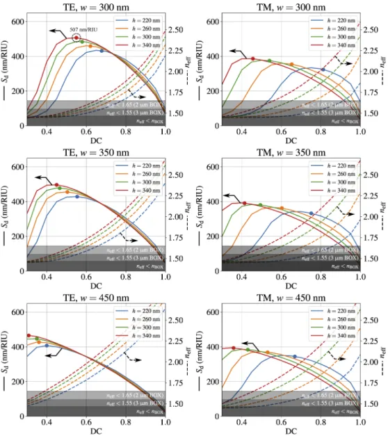
As discussed in the previous section, the device bulk sensitivity can be estimated from the characteristics of the unperturbed waveguide. Thus, the design method relies on finding the dimensions of the SWG waveguide which maximizes the sensitivity. To this end, the two factors determining the device bulk sensitivity (i.e. Saand Sw) were separately calculated for a wide range of widths, heights and duty cycles for both TE and TM polarizations. The simulation results are shown in Fig.2. The curves were calculated for the following sets of values: w ∈ [300, 450] nm; h ∈ [220, 340] nm and DC ∈ [0.3, 1.0]. In all cases we assume ΛSWG = 215 nm, which ensures that at λ0= 1310 nm the waveguide core operates in the subwavelength regime. At the operating wavelength, refractive indexes of silicon and silicon dioxide are nSi(λ0)= 3.503 and
nSiO2(λ0)= 1.466, respectively [20]. Water upper cladding refractive index was varied from 1.31 to 1.33 to calculate the waveguide bulk sensitivity, assuming nc,0= nH2O(λ0)= 1.32.
The behavior observed in the curves of waveguide bulk sensitivity Swfor both polarizations is as expected and agrees well with that recently reported for a wavelength of 1550 nm in [7]. The reduction in the duty cycle of the SWG waveguide causes two simultaneous and opposing effects, as a result of the asymmetry in the refractive indexes of BOX and water upper cladding. While the field delocalization causes an increase in Sw, a displacement of the mode towards the BOX tends to decrease Sw. At the point where the two effects compensate each other, the waveguide sensitivity reaches a maximum. The value of maximum waveguide sensitivity and the duty cycle at which it is reached depends on the ratio h/w. By selecting a high h/w ratio for TE polarization, it is possible to achieve waveguide sensitivity values higher than unity for duty cycles close to 50 %, which is preferred for manufacturability. Concerning architecture sensitivity Sa, the calculated curves show that it monotonically decreases as the field confinement increases, which is expected since Sais inversely proportional to the group index [Eq. (9)].
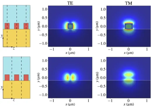
By multiplying the sensitivities Saand Sw, the final device bulk sensitivity Sdis obtained. In Fig.3, Sdcurves are shown along with the effective index for the same dimensions as in Fig.2. An infinite BOX was used in our simulations. This does not imply a practical limitation as it allows us to determine the BOX-thickness (2 µm or 3 µm) that could be used for each combination of parameters while maintaining negligible leakage loss. This is achieved, as experimentally demonstrated in [26], by ensuring that the effective index of the fundamental Floquet-Bloch mode is above 1.65 and 1.55, for a BOX thickness of 2 µm and 3 µm, respectively. For each width and height, the DC that yields the maximum sensitivity while keeping neff>1.55 is indicated with a solid dot. As can be seen, a remarkably high value of 507 nm/RIU is obtained, for w = 300 nm,
h= 340 nm, DC = 55 % and TE polarization.
Comparing both polarizations, it is observed that TM polarization attains lower values of sensitivity and is less affected by changes in the dimensions of the silicon blocks. This is because the TM mode has a larger portion of field traveling inside the BOX compared to the TE mode, as can be seen in Fig.4, where their respective electric field profiles are plotted for the case of the maximum sensitivity.
Fig. 2.SWG waveguide (solid, left axis) and Bragg grating architecture (dashed, right axis) sensitivities computed for TE and TM modes and different geometries. We use a constant pitch ΛSWG= 215 nm to ensure the SWG regime. The operating wavelength is 1310 nm. The sensitivity of the TM mode is less affected by dimensions variation compared to the TE mode. For the latter, the waveguide bulk sensitivity can exceed 1 RIU/RIU when increasing the ratio h/w.
Fig. 3. Device bulk sensitivity curves (solid, left axis) calculated as a product of curves presented in Fig.2and effective index curves of the unperturbed waveguide (dashed, right axis). The dots in different sensitivity curves indicate the points where maximum sensitivity is achieved while keeping leakage loss negligible for a BOX thickness of 3 µm (i.e. neff>1.55).
Due to the invariability of TM polarization waveguide sensitivity, device sensitivity is limited to 400 nm/RIU. With the TE mode, the sensitivity as high as 507 nm/RIU can be achieved (w = 300 nm, h = 340 nm) for the duty cycle near 0.5, the latter facilitating the fabrication of the structure.
Fig. 4.Calculated electric field amplitude of the TE and TM fundamental Floquet-Bloch modes of the SWG waveguide. The dimensions of the waveguide are w = 300 nm, h = 340 nm, DC = 55 % (TE) and w = 450 nm, h = 340 nm, DC = 35 % (TM), ΛSWG= 215 nm. The effective index is 1.55 for both polarizations. Note that the TM mode has a substantial part of the field intensity in the BOX layer, hence not interacting with the analyte. The TE field has a larger overlap with the analyte (upper cladding) region, leading to a higher sensitivity. The maximum sensitivities are 507 nm/RIU and 387 nm/RIU for TE and TM, respectively.
4.2. Bragg filter design and sensor validation
The next step in our design flow is determining the parameters of the Bragg grating. Using Eq. (1) and the effective index of the optimal geometry determined in the previous section (i.e.
neff = 1.55), the Bragg pitch is set to ΛB = 422 nm. The loss coefficient of water at 1310
nm is αc = 76.9 m−1[20] so that the loss constant of the fundamental mode is estimated as α ≈ Swαc= 71.5 m−1. Using |Γ|2
∞= 0.25 (see Table1for other reflectance values), from Eq. (6) we obtain the coupling coefficient κ = 95.3 m−1which corresponds to a 3-dB bandwidth of 27 pm, or, equivalently, a Q factor of 4.9 × 10⁴. To simplify the design, we initially set the lateral block size to t × u = 100 nm × 100 nm for compatibility with deep-UV lithography. Then, by using MPB simulations, the separation s is swept until the desired bandgap is obtained. We have determined that the bandgap is achieved for s = 0.95 µm. We used a grid resolution of 200 px/µm and a convergence tolerance of 10−7. Using Eq. (12), an iLoD of 5.1 × 10⁻⁵RIU was determined. In order to reach the desired reflectance, the required length of the Bragg grating is on the order of 23 mm. Note that this makes it impractical to corroborate these results using an FDTD simulator, underscoring the relevance of the CMT model used in this work. For practical implementation and efficient utilization of wafer area spiral waveguides can be used [33,34]. The phase distortion caused by the effective index dependence on the bending radius can be compensated at the design stage [34]. Using this technique, we estimate the footprint of the sensor to be approximately 430 × 430 µm2.
Table 1. Dependence of the sensor parameters on the reflectance requirement at the resonance wavelength. |Γ |2∞ κ (m−1) ∆λ3dB(pm) iLoD (×10−5RIU) L(cm) 0.75 495.37 118 23.3 0.58 0.5 202.2 49 9.7 1.3 0.25 95.3 27 5.1 2.3
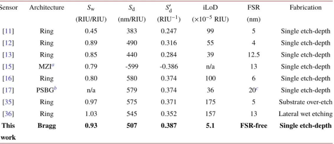
We calculated the reflection spectra from the effective index curves of the unperturbed waveguide neff(nc, λ). The effective index was computed with MPB in a wavelength range of 1310 nm ± 15 nm for cladding refractive indexes from 1.30 to 1.34. These curves together with the aforementioned parameters were introduced in Eq. (2) to calculate |Γ(nc, λ)|2. To verify the design, the whole perturbed structured is introduced in MPB to calculate the bandgap of the fundamental TE Floquet-Bloch mode, for the same set of ncvalues. The results calculated by these two methods are shown in Fig.5. The shift of the resonance wavelength agrees well in both cases, corroborating the design approach used in this work. Table2summarizes the performance of a representative set of recently published SWG-based sensors with experimental validation, including in the last row our simulation results to ease the comparison. The Bragg grating sensor designed in this work is inherently FSR-free, highly competitive in terms of sensitivity (507 nm/RIU) and exhibits a substantial improvement in iLoD (5.1 × 10⁻⁵), thus confirming the potential of this approach and offering promising prospects for using SWG waveguides as refractive index sensors.
Fig. 5. Reflectance curves obtained with CMT model (in colors) for nc ∈ [1.30, 1.34] and resonance wavelength as a function of nc(black line) calculated with MPB bandgap
simulations. In both cases the calculated sensitivities agree with the designed value, Sd=
507 nm/RIU. Note that the typical Bragg grating sidelobes in the spectra vanish due to the water absorption.
A tolerance study showed that varying ±10 nm the geometrical parameters w, a, t and u only causes a 2 % reduction in the device sensitivity and a ±3 × 10⁻⁵RIU change in the iLoD, while the resonance wavelength experiments a ±30 nm shift.
Table 2. Comparison with other TE-polarized SWG-based sensors of the bibliography. Sensor Architecture Sw Sd S′
d iLoD FSR Fabrication
(RIU/RIU) (nm/RIU) (RIU−1) (×10−5RIU) (nm)
[11] Ring 0.45 383 0.247 99 5 Single etch-depth
[12] Ring 0.89 490 0.316 55 4 Single etch-depth
[13] Ring 0.85 440 0.284 39 12.5 Single etch-depth [15] MZIa 0.79 -599 -0.386 n/a 13 Single etch-depth
[16] Ring 0.80 580 0.374 100 6 Single etch-depth [17] PSBGb n/a 579 0.374 36 20c Single etch-depth
[35] Ring 0.97 575 0.371 175 5 Substrate over-etch [36] Ring 1.03 545 0.352 157 13 Lateral wet etching This Bragg 0.93 507 0.387 5.1 FSR-free Single etch-depth work
aMach Zehnder interferometer bPhase shifted Bragg grating cBandgap structure
5. Conclusions
The bulk sensing performance of a novel narrowband subwavelength engineered Bragg grating has been studied. The topology is based on a subwavelength grating waveguide core evanescently coupled to periodic lateral loading segments forming a Bragg filter structure. We use the operating wavelength of 1310 nm, since water-based analyte absorption is lower than at 1550 nm. A comprehensive procedure for designing the device has been devised: first dimensioning the SWG central waveguide to maximize the device sensitivity and then determining the size and location of the loading segments to achieve the targeted filter response, including central wavelength and bandwidth. The calculated results, including sensitivity Sd = 507 nm/RIU and intrinsic limit of detection iLoD = 5.1 × 10⁻⁵RIU, were obtained by the perturbational theory and compared with 3D simulations of the bandgap of the complete sensing structure, yielding good agreement. Compared to other sensing architectures, our device shows remarkable characteristics including a 10-fold reduction in intrinsic limit of detection and an increased dynamic range, the latter circumventing the free spectral range limit of conventional devices. We believe that these results open exciting prospects for future implementation of this new concept in more complex photonic architectures for on-chip biochemical sensing.
A. Sensitivity in Bragg-type sensors
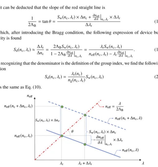
Figure6illustrates the operation of weak Bragg gratings. In a first step, the variation of effective index as a function of the wavelength of the fundamental mode of the unperturbed waveguide is calculated in the vicinity of the resonance wavelength (λr)for two different values of cladding refractive index. This is shown in Fig.6with blue solid and dashed lines for ncand nc+ ∆nc, respectively. Then, the red line corresponds to the Bragg condition [Eq. (1)], whose slope is given by
1 2ΛB =
neff(nc, λr)
λr . (17)
Superposing it in Fig.6allows us to determine the wavelength shift that the spectral response of the Bragg filter will experience when the cladding refraction index varies from ncto nc+ ∆nc. Assuming that both curves of effective index have a linear wavelength dependence and have the same slope, i.e., they only differ by a displacement factor equal to Sw(nc, λr) × ∆ncas shown in
Fig.6, it can be deducted that the slope of the red straight line is 1 2ΛB = tan θ = Sw(nc, λr) × ∆nc+∂n∂λeff |︁ |︁ nc,λr× ∆λr ∆λr (18)
from which, after introducing the Bragg condition, the following expression of device bulk sensitivity is found Sd(nc, λr) ≈ ∆λr ∆nc = 2ΛBSw(nc, λr) 1 − 2ΛB∂n∂λeff |︁ |︁ nc,λr = λrSw(nc, λr) neff(nc, λr) −λr∂neff ∂λ |︁ |︁ nc,λr . (19) Finally, recognizing that the denominator is the definition of the group index, we find the following expression
Sd(nc, λr)= λr(nc)
ng(nc, λr)Sw(nc, λr) (20) which is the same as Eq. (10).
Fig. 6.Graphical demonstration of the expression of sensitivity for sensors based on weak Bragg gratings. The blue lines represent the curves of effective index versus the wavelength of the unperturbed waveguide (in our case the SWG waveguide) for two different and very close values of cladding refractive index, ncand nc+ ∆nc. The red dash-dot line represents
the Bragg condition.
Although the demonstration has been carried out under the assumption that the perturbation is weak, this does not imply a loss of generality. The modification of the effective index curves of the perturbed guide neff with respect to the unperturbed one neff,uwill only result in a displacement of the resonance wavelength, which can be readily corrected by modifying the resulting period ΛBso that the Bragg condition is maintained at the wavelength of interest
λr= 2ΛBneff,u(nc, λr)= 2Λ′Bneff(nc, λr). (21) Funding
Ministerio de Economía y Competitividad (PID2019-106747RB-I00, TEC2016-80718-R); Junta de Andalucía (P18-RT-1453, P18-RT-793, UMA18- FEDERJA-219); Universidad de Málaga; Grantová Agentura České Republiky (19-00062S).
Disclosures
References
1. E. Luan, H. Shoman, D. M. Ratner, K. C. Cheung, and L. Chrostowski, “Silicon photonic biosensors using label-free detection,”Sensors18(10), 3519 (2018).
2. M. Soler, O. Calvo-Lozano, M.-C. Estevez, and L. M. Lechuga, “Nanophotonic Biosensors: Driving Personalized Medicine,”Opt. Photonics News31(4), 24 (2020).
3. K. E. Zinoviev, A. B. Gonzalez-Guerrero, C. Dominguez, and L. M. Lechuga, “Integrated Bimodal Waveguide Interferometric Biosensor for Label-Free Analysis,”J. Lightwave Technol.29(13), 1926–1930 (2011).
4. J. Leuermann, A. Fernández-Gavela, A. Torres-Cubillo, S. Postigo, A. Sánchez-Postigo, L. M. Lechuga, R. Halir, and Í. Molina-Fernández, “Optimizing the limit of detection of waveguide-based interferometric biosensor devices,”
Sensors19(17), 3671 (2019).
5. T. Claes, J. G. Molera, K. D. Vos, E. Schacht, R. Baets, and P. Bienstman, “Label-Free Biosensing With a Slot-Waveguide-Based Ring Resonator in Silicon on Insulator,”IEEE Photonics J.1(3), 197–204 (2009). 6. S. Janz, D.-X. Xu, M. Vachon, N. Sabourin, P. Cheben, H. McIntosh, H. Ding, S. Wang, J. H. Schmid, A. Delâge,
J. Lapointe, A. Densmore, R. Ma, W. Sinclair, S. M. Logan, R. MacKenzie, Q. Y. Liu, D. Zhang, G. Lopinski, O. Mozenson, M. Gilmour, and H. Tabor, “Photonic wire biosensor microarray chip and instrumentation with application to serotyping of Escherichia coliisolates,”Opt. Express21(4), 4623–4637 (2013).
7. J. G. Wangüemert-Pérez, A. Hadij-ElHouati, A. Sánchez-Postigo, J. Leuermann, D.-X. Xu, P. Cheben, A. Ortega-Mo nux, R. Halir, and Í. Molina-Fernández, “[INVITED] Subwavelength structures for silicon photonics biosensing,”
Opt. Laser Technol.109, 437–448 (2019).
8. Í. Molina-Fernández, J. Leuermann, A. Ortega-Mo nux, J. G. Wangüemert-Pérez, and R. Halir, “Fundamental limit of detection of photonic biosensors with coherent phase read-out,”Opt. Express27(9), 12616 (2019).
9. A. Densmore, D. Xu, P. Waldron, S. Janz, P. Cheben, J. Lapointe, A. Delge, B. Lamontagne, J. H. Schmid, and E. Post, “A Silicon-on-Insulator Photonic Wire Based Evanescent Field Sensor,”IEEE Photonics Technol. Lett.18(23), 2520–2522 (2006).
10. K. D. Vos, “Label-free Silicon Photonics Biosensor Platform with Microring Resonators,” Ph.D. thesis, Universiteit Gent (2010).
11. V. Donzella, A. Sherwali, J. Flueckiger, S. M. Grist, S. T. Fard, and L. Chrostowski, “Design and fabrication of SOI micro-ring resonators based on sub-wavelength grating waveguides,”Opt. Express23(4), 4791–4803 (2015). 12. J. Flueckiger, S. Schmidt, V. Donzella, A. Sherwali, D. M. Ratner, L. Chrostowski, and K. C. Cheung, “Sub-wavelength
grating for enhanced ring resonator biosensor,”Opt. Express24(14), 15672–15686 (2016).
13. H. Yan, L. Huang, X. Xu, S. Chakravarty, N. Tang, H. Tian, and R. T. Chen, “Unique surface sensing property and enhanced sensitivity in microring resonator biosensors based on subwavelength grating waveguides,”Opt. Express
24(26), 29724 (2016).
14. L. Huang, H. Yan, X. Xu, S. Chakravarty, N. Tang, H. Tian, and R. T. Chen, “Improving the detection limit for on-chip photonic sensors based on subwavelength grating racetrack resonators,”Opt. Express25(9), 10527 (2017). 15. M. Odeh, K. Twayana, K. Sloyan, J. E. Villegas, S. Chandran, and M. S. Dahlem, “Mode Sensitivity Analysis of
Subwavelength Grating Slot Waveguides,”IEEE Photonics J.11(5), 1–10 (2019).
16. E. Luan, H. Yun, L. Laplatine, Y. Dattner, D. M. Ratner, K. C. Cheung, and L. Chrostowski, “Enhanced Sensitivity of Subwavelength Multibox Waveguide Microring Resonator Label-Free Biosensors,”IEEE J. Sel. Top. Quantum Electron.25(3), 1–11 (2019).
17. E. Luan, H. Yun, M. Ma, D. M. Ratner, K. C. Cheung, and L. Chrostowski, “Label-free biosensing with a multi-box sub-wavelength phase-shifted Bragg grating waveguide,”Biomed. Opt. Express10(9), 4825–4838 (2019). 18. J. G. Wangüemert-Pérez, P. Cheben, A. Ortega-Moñux, C. Alonso-Ramos, D. Pérez-Galacho, R. Halir, Í.
Molina-Fernández, D.-X. Xu, and J. H. Schmid, “Evanescent field waveguide sensing with subwavelength grating structures in silicon-on-insulator,”Opt. Lett.39(15), 4442–4445 (2014).
19. L. Torrijos-Morán, A. Griol, and J. García-Rupérez, “Experimental study of subwavelength grating bimodal waveguides as ultrasensitive interferometric sensors,”Opt. Lett.44(19), 4702–4705 (2019).
20. M. Polyanskiy, “Refractive Index database,” (2020).https://refractiveindex.info.
21. P. Cheben, R. Halir, J. H. Schmid, H. A. Atwater, and D. R. Smith, “Subwavelength integrated photonics,”Nature
560(7720), 565–572 (2018).
22. J. Čtyroký, J. G. Wangüemert-Pérez, P. Kwiecien, I. Richter, J. Litvik, J. H. Schmid, Í. Molina-Fernández, A. Ortega-Moñux, M. Dado, and P. Cheben, “Design of narrowband Bragg spectral filters in subwavelength grating metamaterial waveguides,”Opt. Express26(1), 179–194 (2018).
23. P. Cheben, J. Čtyroký, J. H. Schmid, S. Wang, J. Lapointe, J. G. Wangüemert-Pérez, Í. Molina-Fernández, A. Ortega-Moñux, R. Halir, D. Melati, D. Xu, S. Janz, and M. Dado, “Bragg filter bandwidth engineering in subwavelength grating metamaterial waveguides,”Opt. Lett.44(4), 1043–1046 (2019).
24. C. Chen, Foundations for guided-wave optics (John Wiley & Sons, 2007).
25. R. Halir, P. J. Bock, P. Cheben, A. Ortega-Moñux, C. Alonso-Ramos, J. H. Schmid, J. Lapointe, D.-X. Xu, J. G. Wangüemert-Pérez, Í. Molina-Fernández, and S. Janz, “Waveguide sub-wavelength structures: a review of principles and applications,”Laser Photonics Rev.9(1), 25–49 (2015).
26. J. D. Sarmiento-Merenguel, A. Ortega-Moñux, J.-M. Fédéli, J. G. Wangüemert-Pérez, C. Alonso-Ramos, E. Durán-Valdeiglesias, P. Cheben, Í. Molina-Fernández, and R. Halir, “Controlling leakage losses in subwavelength grating silicon metamaterial waveguides,”Opt. Lett.41(15), 3443–3446 (2016).
27. K.-S. Lim, H.-Z. Yang, A. Becir, M.-H. Lai, M. M. Ali, X. Qiao, and H. Ahmad, “Spectral analysis of bent fiber Bragg gratings: theory and experiment,”Opt. Lett.38(21), 4409–4412 (2013).
28. M. C. Estevez, M. Alvarez, and L. M. Lechuga, “Integrated optical devices for lab-on-a-chip biosensing applications,”
Laser Photonics Rev.6(4), 463–487 (2012).
29. I. M. White and X. Fan, “On the performance quantification of resonant refractive index sensors,”Opt. Express16(2), 1020–1028 (2008).
30. L. Chrostowski, S. Grist, J. Flueckiger, W. Shi, X. Wang, E. Ouellet, H. Yun, M. Webb, B. Nie, Z. Liang, K. C. Cheung, S. A. Schmidt, D. M. Ratner, and N. A. F. Jaeger, “Silicon photonic resonator sensors and devices,”Laser Resonators, Microresonators, and Beam Control XIV8236, 823620 (2012).
31. T. Yoshie, L. Tang, and S.-Y. Su, “Optical microcavity: Sensing down to single molecules and atoms,”Sensors11(2), 1972–1991 (2011).
32. S. G. Johnson and J. D. Joannopoulos, “Block-iterative frequency-domain methods for Maxwell’s equations in a planewave basis,”Opt. Express8(3), 173–190 (2001).
33. Z. Chen, J. Flueckiger, X. Wang, F. Zhang, H. Yun, Z. Lu, M. Caverley, Y. Wang, N. A. F. Jaeger, and L. Chrostowski, “Spiral Bragg grating waveguides for TM mode silicon photonics,”Opt. Express23(19), 25295–25307 (2015). 34. A. D. Simard, Y. Painchaud, and S. LaRochelle, “Integrated Bragg gratings in spiral waveguides,”Opt. Express
21(7), 8953–8963 (2013).
35. E. Luan, K. M. Awan, K. C. Cheung, and L. Chrostowski, “High-performance sub-wavelength grating-based resonator sensors with substrate overetch,”Opt. Lett.44(24), 5981–5984 (2019).
36. C.-W. Chang, X. Xu, S. Chakravarty, H.-C. Huang, L.-W. Tu, Q. Y. Chen, H. Dalir, M. A. Krainak, and R. T. Chen, “Pedestal subwavelength grating metamaterial waveguide ring resonator for ultra-sensitive label-free biosensing,”
![Fig. 1. Top and perspective view of the Bragg filter structure proposed in [22] and experimentally demonstrated in [23] that has been analyzed as a sensor in this paper.](https://thumb-eu.123doks.com/thumbv2/123doknet/13997441.455595/3.918.241.671.748.932/perspective-bragg-filter-structure-proposed-experimentally-demonstrated-analyzed.webp)