Submitted to the Department of Materials Science and Engineering
in partial fulfillment of the requirements for the degree of
Master of Science in Materials Science and Engineering
at the
MASSACHUSETTS INSTITUTE OF TECHNOLOGY
May 1994
Nicole Danielle B. Lazo, MCMXCIV. All rights reserved.
The author hereby grants to MIT permission to reproduce and distribute publicly paper and electronic copies of this thesis document in whole or in part, and to grant others theright to do so.
Author
. . . ... f W. . . . .Department of Materials Science and Engineering
-,-- I '0 Z . M ay 6, 1994
Certified by .... L'.
... I...I...Ir
....
er of Technical Staff,
.1 . I. . . .
Eugene A. Fitzgerald
AT&T Bell Laboratories
Thesis Supervisor
C
ertified
by
... -.
... ...
Lionel C. Kimerfing
Professor, Department of Materials Science and Engineering
Thesis Supervisor
A ccepted by ...
IN%
...
Carl V. Thompson
Professor of Electronic Materials
Chairman, Departmental Committee on Graduate Students
44""'T i'TiJ "'E
Design and Implementation of Top-Contact
Light-Emitting Diodes Integrated on Silicon
by
Design and Implementation of Top-Contact Light-Emitting
Diodes Integrated on Silicon
by
Nicole Danielle B. Lazo
Submitted to the Department of Materials Science and Engineering on May 6 1994, in partial fulfillment of the
requirements for the degree of
Master of Science in Materials Science and Engineering
Abstract
III-V integration on Si potentially has many optoelectronic applications. Among these is the production of LEDs on a Si substrate. InGaP red LEDs integrated on Si have already been demonstrated. However, those devices utilized contacts to the backside. This thesis details work accomplished towards the design and manufacture of top-contact LEDs from InGaP grown on a Si substrate using a graded GeSi inter-layer. In the pursuit of this goal, the necessary masks and a processing recipe were designed. This report focuses particularly on contact formation to InGaP LEDs on both GaAs and Si substrates and includes cross-sectional transmission electron micro-scopic analysis of both starting materials. We succeeded in making top-contact InGaP red (-640 nm) LEDs on a GaAs substrate. Examination of current-voltage curves indicate that the devices on the Si substrate failed due to contacts spiking through the active region. We expect to skirt this problem by performing separate anneals of the two contacts. The work for this thesis was done at AT&T Bell Laboratories in Murray Hill, NJ, under the MIT III-B internship program.
Thesis Supervisor: Eugene A. Fitzgerald
Title: Member of Technical Staff, AT&T Bell Laboratories Thesis Supervisor: Lionel C. Kinierling
Many, many thanks to Dr. Eugene Fitzgerald who taught me almost everything that I needed to know, but didn't know yet, for this project. Gene, I was very lucky to have you as my mentor. I really appreciated your giving my project much thought even before I showed up, your taking the time to explain many things clearly to me and your support throughout my stay at AT&T (that continues to the present). Thanks also for the many enjoyable technical and non-technical discussions. I learned much and had a lot of fun along the way. Kudos to you too for having survived 7 months of working with me and the last few weeks of paranoia.
I am grateful to Prof. Lionel Kimerling for many helpful suggestions. I want to ex-press my appreciation to Dr. G. Patrick Watson for many ideas regarding processing, Tom Sorsch for teaching me TEM sample preparation and many discussions, Paul Silverman for furnace annealing my samples, Dr. Ya-Hong Xie and Dr. Joe Wiener for help in mask design, Ted Fulton for making the masks, Dr. Stephen Pearton and Jim Lothian for plasma etching my InGaP samples, and John Filipe and Ralph DeClassis for the use of the RTA.
Thanks to the wonderful people at MIT, AT&T and elsewhere whom I have the honor of calling my friends, for visits, phone calls, letters, e-mail, discussions and zwrites that made not only my stay at AT&T, but also my years at MIT, a wonderful mix of hard work and fun. I would never have been able to maintain my (in)sanity without you.
And finally, to my family, both in the Philippines and in Washington, DC, whose love and support I can always rely on. There are many things that have happened in my life for which I feel very fortunate. The first of those is my having been born into such a caring and understanding family. Thank you for making a visit home something that I always look forward to.
Contents
I
Introduction 82 Theoretical Background 10
2.1 Previous Work on InGaP LEDs . . . 10
2.2 III-V Integration on Si using GeSi interlayers . . . 11
2.3 Antiphase Boundary Formation . . . 12
3 Experimental Design 14 3.1 XTEM Sample Preparation . . . 14
3.2 XTEM Analysis of Starting Material . . . 15
3.2.1 Fabrication of InGaP/GaAs and InGaP/GaAs/Ge/Si Starting M aterial . . . 15
3.2.2 XTEM of InGaP/GaAs . . . 17
3.2.3 XTEM of InGaP/GaAs/Ge/Si . . . 18
3.3 M ask Design . . . 20
3.4 Processing . . . 23
4 Results and Discussion 27 4.1 InGaP/GaAs Devices . . . 28
4.2 InGaP/GaAs/Ge/Si Devices . . . 37
List of Figures
2-1 Formation of antiphase boundaries (APB) due to deposition of less than a full monolayer of Ga on the Ge epitaxial layer, which serves as
a tem plate . . . 13
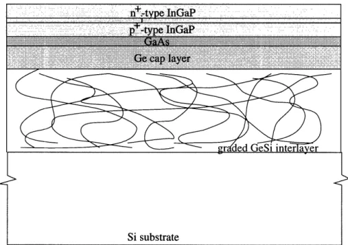
3-1 Cross-sectional diagram of InGaP/GaAs/Ge/Si starting material. A 100 A GaAs layer was deposited on the n-type InGaP layer but is
not specifically labelled in this figure . . . 16
3-2 Diagram of cross-section of InGaP/GaAs sample. The InGaP layer is the same as in Figure 31 A 0 A GaAs layer was deposited on the n+-type InGaP layer but not specifically labelled in this figure. . . . 16 3-3 XTEM micrograph of a region typical of most areas of the InGaP/GaAs
sample. The dark spots on the InGaP layer are the In-balls formed during ion milling of the sample. Above the InGaP layer are -3000 A of photoresist and -1000 A of gold. The pale smudge at the bottom center of the micrograph is from the electron micrograph film. Below the InGaP layer are the GaAs substrate and the GaAs epitaxial layer
deposited prior to InGaP growth . . . 17
3-4 XTEM micrograph of InGaP/GaAs showing a dislocation cluster
nu-cleating from a point on the GaAs/GaAs homointerface . . . 18
3-5 XTEM micrograph of InGaP/GaAs/Ge/Si sample from the edge of the wafer. Note that the Ge cap layer is absent and that dislocations from
3-6 XTEM micrograph of a sample from the InGaP/GaAs/Ge/Si wafer's center. At the bottom of the micrograph is the top of the Ge cap layer and GaAs epitaxial layer. In the upper center is the 1.5 pm InGaP layer. No threading dislocations extending into the InGaP layer were
observed . . . 20
3-7 XTEM micrograph of an antiphase boundary at the GaAs/GaAs ho-mointerface in the InGaP/GaAs/Ge/Si sample using the 220)
two-beam condition . . . 21
3-8 Schematic of the mask design. Not the entire bonding pads are shown. 22 3-9 Schematic of the cross-section of an InGaP/GaAs/Ge/Si device. . . . 24
4-1 Diagram of contact/probe locations .. . . . 28
4-2 Current-voltage curve of InGaP/GaAs light-emitting diode in forward bias when probing the top contacts. The diodes emit light to the eye
at an applied voltage of 35 V . . . 29
4-3 Current-voltage curve of InGaP/GaAs light-emitting diode in reverse
bias when probing the top contacts . . . 30
4-4 Current-voltage curve for InGaP/GaAs device when probing the lower contact and the backside. The lower contact displays ohmic behavior. 32 4-5 Current-voltage curve for InGaP/GaAs light-emitting diode when the
upper contact and backside are probed . . . 33
4-6 SEM micrograph of a 100 tim-diameter InGaP/GaAs diode. Note the
varying brightness of the lower contact . . . 34
4-7 SEM micrograph of the same diode as in Figure 46 but as seen from an angle. Note the presence of bubbles in the lower contact that caused
the contrast variation in Figure 46 . . . 35
4-8 Cathodoluminescence spectrum of a red light-emitting InGaP/GaAs diode. The peaks at 640 nm and 860 nm are due to the InGaP epitaxial
4-9 Map of cathodoluminescence data of an InGaP/GaAs diode. The
whiter the region, the higher the intensity of emitted light . . . 36
4-10 Current-voltage curve typical of most of the InGaP/GaAs/Ge/Si
de-vices when the top contacts are probed . . . 38
4-11 Current-voltage curve of the InGaP/GaAs/Ge/Si device when probing the lower contact and backside. This indicates that the lower contact
is bonded to the p-type layer, as planned . . . 39
4-12 Current-voltage curve of InGaP/GaAs/Ge/Si device when probing the upper contact and backside. This implies that Au from the upper
contact has spiked through the active region . . . 40
4-13 Current-voltage curve of an InGaP/GaAs/Ge/Si device prior to "burn
Chapter
Introduction
Integration of IIIN materials on silicon is a dream, that if successful, will allow production of Si and III-V-based optoelectronic devices on the same chip. The goal of this work is to design and manufacture arrays of top-contact light-emitting diodes (LEDs) integrated on Si. There are three reasons for doing this. The first is reverse doping. When a IIIN material is grown on Si, the group III element tends to diffuse into the Si and dope it p-type. In turn, Si diffuses into the IIIN compound and makes it n-type. This can cause back-to-back diodes if a regular (the topmost layer is p-type) diode is made and the backside is contacted, making the current flow through the III-V/IV interface. Using top contacts would allow the current to avoid this interface altogether. In addition, we try to circumvent this problem by producing an inverse (n-type layer is topmost) diode on a p-type substrate. Second, dislocations generally trap carriers so we expect the dislocated, graded region to have a high resistance. Passing the current through this region would negatively affect the performance of the LED by increasing the series resistance to the device. The higher series resistance would raise the threshold voltage at which the diode emits light. Finally, current microelectronics standards require that devices function atop a floating or undoped substrate. As before, conducting through the backside in such a situation would impair the performance of the LED.
Red light-emitting diodes (InGaP lattice matched to GaAs) contacted from the backside had already been manufactured 6 before this work commenced. InGaP
homojunctions with a thinner intrinsic layer (1000 A instead of 500 A had been grown but attempts to make LEDs from this material using contacts to the backside were unsuccessful. This drove us to focus on making top-contact LEDs. We hoped to be able to make top-contact arrays of these devices so that we could determine their mean time to failure as well as demonstrate the feasibility of making LEDs integrated
on Si.
This document first discusses previous work done with InGaP LEDs as well as the research leading up to IIIN integration on Si. It subsequently details what was accomplished at AT&T including mask design, cross-sectional TEM analysis of the material and processing developments, with emphasis on contact formation. It con-cludes with an analysis of resulting current-voltage curves and cathodoluminescence spectrum of the devices.
Chapter 2
Theoretical Background
There is much interest in II-VI compounds because many emit light in the visible range. III-V ompounds, on the other hand, generally emit light in the infrared regime. An exception to this is In,,,Gal-.,P, which has a direct bandgap at composi-tions corresponding to the range from red to yellow-green light in the visible spectrum. The values of x at the extremes of this range are 0.5 and 032 which have lattice pa-rameters equal to those of Ge and GeO.7SiO.3, respectively. The capability to make
visible light-emitting diodes (LEDs) from III-V materials which is a more mature technology than II-VI compounds, was tempting. Hence, we focussed our efforts on InGaP LEDs using GeSi interlayers.
2.1 Previous Work on InGaP LEDs
There have been a number of publications on InGaP LEDs. Kondo and associates [51 fabricated InGaP orange LEDs on a Si substrate using aAsP/GaAs buffer layers.
The devices had a dislocation density of 108 /CM 2 yet operated for 2000 hours at an
injection current of 500 A/CM2. Chen and co-workers 3 report the manufacture of
InGaP yellow-green LEDs on a GaAs substrate utilizing a graded GaAsP buffer layer. Stinson and collaborators 14] produced InGaP LEDs on a GaP substrate using a graded InGaP layer. Two groups [8, 15] made single heterojunction AlGaAs/InGaP red LEDs lattice matched to a GaAs substrate. All studies used contacts to the
backside. Most employed IIIN substrates and the one that utilized a Si substrate had a high dislocation density which is expected to adversely affect the long term performance of the devices.
2.2 III-V Integration on Si using GeSi interlayers
For LED integration with silicon technology, it is desirable to be capable of growing IIIN epitaxial layers with a low dislocation density on a silicon substrate. To do so, one must increase the lattice constant of epitaxial layers on Si while minimizing the formation of threading dislocations which extend up into the layers. Fitzgerald and co-workers 4 report of such layers made of Ge,,,Sil-,,. Ge and Si are completely miscible in each other. hat is, a Ce,,Sil-,,, compound of any composition forms a single phase and does not separate into Ge-rich and Si-rich regions. Changes of composition bring about changes in lattice parameter. The lattice parameter increases linearly with Ge concentration. The ability to grow high quality GeSi on a Si substrate would have two consequences. First, it would be possible to integrate materials with larger lattice constants than that of Si on a Si substrate. Second, the lattice constant can be tailored to anywhere between that of Si and Ge. Fitzgerald and associates 4 succeeded in growing GeSi layers with a dislocation density of about 10'/cm 3 on Si. They
accomplished this using solid-source molecular beam epitaxy of linearly graded GeSi at 9000C. Growth is executed at this rather high temperature to minimize the number of dislocations which thread up into the epitaxial layer. These threading dislocations nucleate easily then they glide and form misfit dislocations which more effectively relieve the stress in the strained layer. Growth at high temperatures encourages the development oflong misfit dislocations which, in turn, maximizes the amount of stress relieved for every threading dislocation nucleated. This allows the layers to completely relax with relatively few threading dislocations. They found that a grading rate of 10% Ge/pm minimized the dislocation density while yielding a reasonable growth time for the structures. There are two main applications of linearly graded GeSi interlayers that are currently under investigation: two-dimensional electron or hole
gases [10] using strained Si and Ge layers, respectively, and IIIN integration on Si.
This report concentrates on the latter.
Once good quality growth of GeSi on Si had been demonstrated, attempts to use these GeSi layers as virtual substrates for IIIN compounds commenced. First, the mechanics of GaAs growth on Ge was analyzed. GaAs is lattice matched to Ce, so the GeSi interlayer would be graded from pure Si to pure Ce before GaAs is deposited. To study the conditions of growth of GaAs on Ge a Ge virtual substrate was made by depositing pure Ge on a Si substrate. This layer was highly dislocated because of the large lattice mismatch between Si and Ge. However, it sufficed for the examination of GaAs growth on Ge. GaAs was epitaxially grown on the Ge layer via molecular beam epitaxy. The first attempts produced an uneven GaAs surface. Transmission electron microscopy (TEM) indicated that As roughens the Ce surface. Such a surface results in many antiphase boundaries (APB) being formed, as discussed in Section 23. Depositing a fll monolayer of Ca before As was added to the system yielded good quality GaAs since the Ge surface was not allowed to come to equilibrium with As. The lack of antiphase boundaries also prevents the trapping of many dislocations at
the GaAs/Ge interface.
2.3 Antiphase Boundary Formation
We now discuss antiphase boundary formation in more detail. The wafers used were cut 60 off the [001] towards the nearest <111>. The angle offcut is large enough that most of the steps on this atomically rough surface are double-height atomic steps, although there are some that are only single-height steps. Because GaAs has a zincblende structure, depositing As first on an area that is on the same level as or one unit cell lower than Ga displaces the unit cell by half (see Figure 2-1). Another way of looking at it is that As atoms in the arsenic-first regions sit on Ga sites or vice versa. This misplacement of atoms in zincblende structures is termed antisite disorder. The two-dimensional boundary formed by Ga-Ca or As-As bonds due to this misplacement is called an antiphase boundary (APB). If less than a full monolayer of Ga is grown
Ga As
Ga-Ga bond
As atom in a Ga site
Figure 21: Formation of antiphase boundaries (APB) due to deposition of less than a full monolayer of Ga on the Ge epitaxial layer, which serves as a template.
before As is released into the system, As may be the first layer deposited on Ge in certain areas, and Ga will be the first layer in the other regions. This causes areas to be displaced by half a unit cell from the material around it. Kuo and colleagues 6] observed antiphase boundaries arising from the Ge/GaAs interface. In addition, they noted that threading dislocations can get pinned by antiphase boundaries.
After accomplishing satisfactory results in growing APB-free GaAs on highly dis-located Ge that was deposited directly on a Si substrate, Kuo and collaborators used a linearly graded region from pure Si to pure Ge with a Ge cap layer as a tem-plate for subsequent GaAs. They obtained good results and proceeded to grow n-i-p
Ino.5Gao.5P, which is lattice matched to GaAs, on the GaAs layer. The n-, i- and
p-type layers were all 5000 A thick with the n-type region being the topmost layer. They succeeded in operating these red LEDs at room temperature using contacts to both the frontside and the backside.
Chapter 3
Experimental Design
The two materials used in this study were: 9 n-i-p Ino.5Gao.5P on p-type GaAs 9 n-i-p InO.5GaO.5P on p-type GaAs/Ge/Si
Both samples were scrutinized under cross-sectional transmission electron mi-croscopy (XTEM) prior to processing. The method of XTEM sample preparation is outlined in Section 31. Details about the starting material will be further discussed in Section 32. Finally, mask design and processing are presented in Sections 33 and 3.4, respectively.
3.1 XTEM Sample Preparation
All three materials were characterized using cross-sectional transmission electron mi-croscopy (XTEM). Preparation of samples for XTEM proceeds in the following man-ner. The sample is cleaved into 2 mm x 3 mm pieces. Epoxy is spread on the top surface of these pieces. Two pieces are then pressed together such that the epoxy layer is sandwiched between the top surfaces of the two layers. The 3 mm face of the sample is anually ground on fine grain silicon carbide paper until the 2 mm width is diminished to about 35 Mm. It is then milled via argon ion bombardment until it is thin enough to be examined under TEM (around m). This is generally
accomplished at room temperature. However, the InGaP samples had to be milled at liquid nitrogen temperature, which prevents the surface InGaP from decomposing and leaving In-.balls on the TEM sample surface.
3.2 XTEM Analysis of Starting Material
3.2.1 Fabrication of InGaP/GaAs and InGaP/GaAs/Ge/Si
Starting Material
The InGaP layer on both the GaAs/Ge/Si and GaAs substrates was grown
simul-taneously after preparation of the GaAs/Ge/Si substrate. The GaAs/Ge/Si virtual
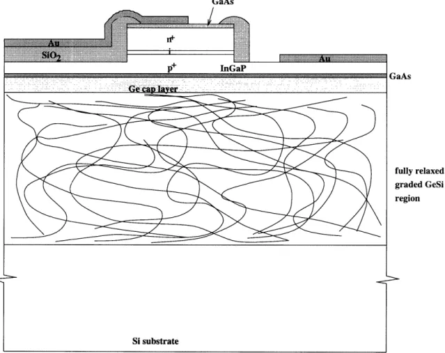
substrate was made by growing a 0 pm thick layer of linearly graded p-type GeSi on a p-type Si substrate to a final concentration of 100% Ge using molecular beam epi-taxy (MBE) (see Figure 31) A 1 pm thick cap layer was subsequently deposited to distance the surface from the buried misfit dislocations. The wafer was polished and transferred to a III-V MBE growth chamber and a 000 A thick layer of p-type GaAs grown on top of it. It was then taken out of the growth chamber and cleaved into 4 pieces for separate experiments. The GaAs and Ge/Si substrates were then cleaned using a HCI dip to remove surface oxide and returned to the growth chamber. The standard clean prior to epitaxial growth was omitted for fear that it may completely etch the 500 A GaAs layer. Another 500 A of p-type GaAs was deposited on top of the initial aAs layer before growth of the p-type lattice-matched Ino.5Gao.5P layer began (see Figures 31 and 32). This was followed by growth of the intrinsic
and n-type layers. Complete records for the InGaP growth are not available so we do not know the thickness of the n- and p-type regions. However, the entire n-i-p InGaP region can be seen to be 1.5 Mm thick in the XTEM micrograph (Figure 33). A thin layer (1000 A) of GaAs was subsequently grown to aid in the formation of an ohmic contact to the n-type layer. Details of the GeSi and InGaP growth procedure are described elsewhere 6.
Figure 31: Cross-sectional diagram of InGaP/GaAs/Ge/Si starting material. A 100 A GaAs layer was deposited on the n-type InGaP layer but is not specifically labelled in this figure.
.pe IhGAP
...
Figure 32: Diagram of cross-section of InGaP/GaAs sample. The InGaP layer is the same as in Figure 31 A 00
A
GaAs layer was deposited on the n-type InGaP layer but not specifically labelled in this figure.Figure 33: XTEM micrograph of a region typical of most areas of the nGaP/GaAs sample. The dark spots on the InGaP layer are the In-balls formed during ion milling of the sample. Above the InGaP layer are 3000
A
of photoresist and-100 A of
gold. The pale smudge at the bottom center of the micrograph is from the electron micrograph film. Below the InGaP layer are the GaAs substrate and the GaAs epitaxial layer deposited prior to InGaP growth.
3.2.2 XTEM of InGaP/GaAs
The XTEM micrograph (in Figure 33) of an InGaP/GaAs sample shows variations in the contrast of the InGaP layer which may be due to spinodal decomposition and/or ordering. TEM micro-diffraction patterns of the InGaP layer around the (111) spots show an insignificant degree of ordering, if any. Hence, the contrast variation is probably due to spinodal decomposition, typical of the InGaP system. The micrograph also evinces good quality (low dislocation density) InGaP growth on GaAs.
Most of the areas of the InGaP/GaAs samples were free of dislocations, which implies a dislocation density less than 108 /CM 2- However, a few areas were found to
have a high density of dislocations (see Figure 34). These dislocations converged to points on the GaAs/GaAs homointerface where the GaAs epitaxial layer directly
beneath the InGaP layer meets the GaAs substrate. The dislocations apparently
Figure 34: XTEM micrograph of InGaP/GaAs showing a dislocation cluster nucle-ating from a point on the GaAs/GaAs homointerface.
Rom this, we conclude that a HCI dip does not clean the surface sufficiently. Should it be necessary to remove the sample from the growth chamber after the initial epitaxial growth of GaAs a thicker initial layer of GaAs has to be grown to permit the use of
the standard clean.
3.2.3 XTEM of InGaP/GaAs/Ge/Si
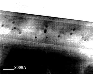
The first XTEM InGaP/GaAs/Ge/Si samples examined were taken from the edge of the wafer. As seen in Figure 35, the pm Ge cap layer is absent and some threading
dislocations from the graded region continue into the InGaP layer. We surmised that the absence of the cap layer was due to the polishing of the sample prior to the deposition of the initial GaAs layer. The mechanical polishing used tends to remove more materialfrom the edge of the wafer than from the center. Figure 35 indicates that the sample was polished into the Ge.,Sil-,,, graded region. We suspected that the threading dislocation problem was caused by the absence of the Ge cap layer for the following reasons. The effective strain at the GaAs/Ge.,Sil-,, interface would be higher because the lattice parameter is not as large as in pure Ge which leads to a larger mismatch with GaAs and increases the likelihood of dislocation nucleation. Also, prior to GaAs deposition, the samples are heated to 650'C to cause GeO2
Figure 35: XTEM micrograph of InGaP/GaAs/Ge/Si sample from the edge of the wafer. Note tat the Ge cap layer is absent and that dislocations from the graded region extend into the InGaP layer.
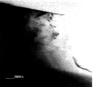
decomposition. However, any Si on the surface bonds strongly with oxygen and the Si-O bond does not break until the temperature is raised to 900'C. Hence, GaAs was grown on an oxide-contaminated surface, because the Ge,,Sil-,, region was exposed, which encourages the formation of dislocations. To confirm this, a sample closer to the center of the wafer was examined (Figure 36). The 1 /tm Ge Cap layer was present and no threading dislocations extending into the InGaP layer were observed. When GaAs is first deposited on Ge, the slow growth rate of 1000 A/hour is used to accurately deposit 11.2 monolayers. The growth rate is increased after 10 minutes to I Lm/hour. To fully control GaAs growth, the MBE system has to be calibrated for both growth situations. The system had not been calibrated for the slower growth rate prior to preparation of our samples. Thus, we suspected the formation of antiphase boundaries at the Ge/GaAs interface due to incomplete Ga coverage of the Ge surface. Close examination of the interface confirmed this prediction (Figure 37). Obtaining good images of the antiphase boundaries proved elusive but we found that the 220) 2-beam diffraction condition provided the best contrast for observation of antiphase boundaries. All the APBs appear to annihilate each other in the lower half of the GaAs layer. Nne were observed to extend throughout the GaAs layer. In some cases,
.. ... ... ... .
Figure 36: XTEM micrograph of a sample from the InGaP/GaAs/Ge/Si wafer's center. At the bottom of the micrograph is the top of the Ge cap layer and GaAs epi-taxial layer. In the upper center is the 1.5 /Lm InGaP layer. No threading dislocations extending into the InGaP layer were observed.
APBs trapped dislocations, as was observed in 6 and prevented them from gliding to relieve strain. Hence, the presence of antiphase boundaries causes an increase in the threading dislocation density, which in turn affects the performance of the device. Therefore, care must be taken to ensure complete coverage of the Ge layer with a Ca monolayer prior to the release of As into the system.
3.3 Mask Design
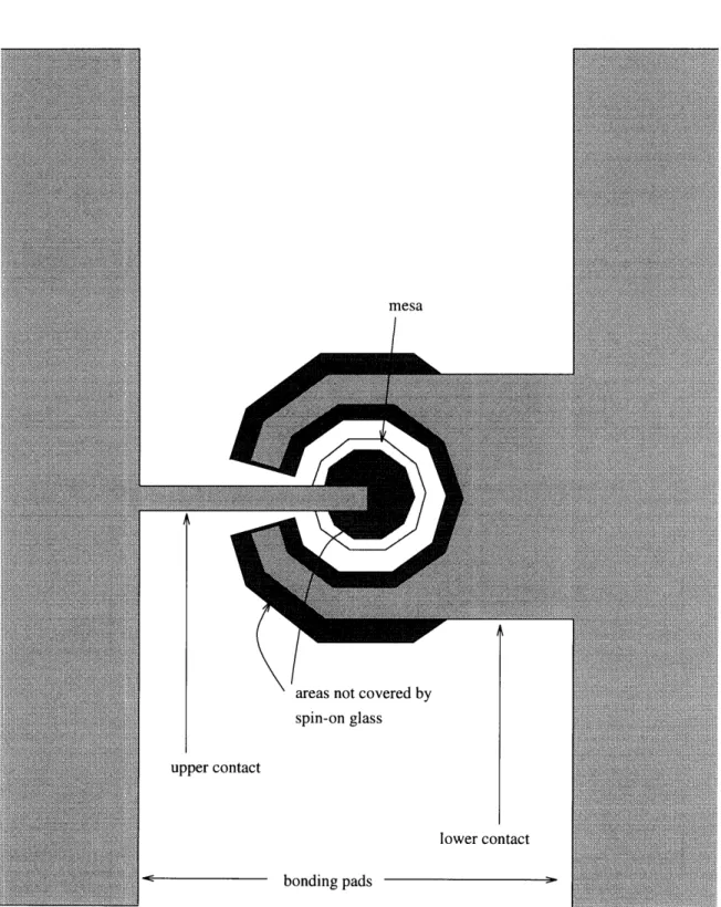
Masks for the production of top-contact LEDs had to be designed and fabricated. The masks were made on a Gyrex machine using Fe2O3 films on a glass substrate.
The design constraint was that there be a maximum of 10,000 areas exposed on each mask, all of which are rectangular. We used Autodesk's Autosketch" to design the masks.
The first mask layer is for the mesa etch device isolation. We made circular LEDs by superposing rectangles, each rotated 36' around the center from the previous one. In the figure, the darkened area shows the portions of the mask which will result
Figure 37: XTEM micrograph of an antiphase boundary at the GaAs/GaAs homoin-terface in the InGaP/GaAs/Ce/Si sample using the 220) two-beam condition. in areas protected by photoresist during etching. The second mask layer is to be used for opening contacts to the n- and p-type layers after an insulating layer of oxide is spun on. The shaded region denotes the areas where the spin-on glass was etched away. The third and fourth mask layers are for evaporation of the lower and upper contacts. The shaded region depicts the sections that will be covered with metal after processing. The metal in the parts that are not covered by spin-on glass are what I subsequently refer to as the contacts; and the large rectangles to the extreme left and right of the figure, the bonding pads. The claw-shaped contact that encircles the mesa is the lower contact. A concern in forming mesas for LEDs is the issue of current crowding which pertains to the increase in resistance when the current flows from a region of large cross-sectional area to one with smaller. The smaller cross-sectional area prevents the current from spreading. By spreading the contact area around the mesa, we hoped to minimize the current crowding effect to the upper contact. We decided to make separate masks for the upper and lower contacts in case their processing differs. It is always possible to align and expose both mask steps and metallize both contacts at the same time. As will be discussed further in the processing section, different procedures were required, so designing separate mask steps for the contacts was an important precaution.
mesa
I
i
ered by areas not cov spin-on glass
upper contact
bonding pads
lower contact
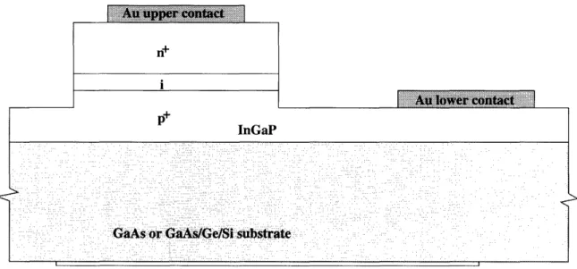
A schematic of" the cross-section of the final product is depicted in Figure 39. Using the first mask, we etched down to the lower layer (p-type) of the active region and formed circular mesas. We first attempted to do so using a :8:100 H2SO4:H202:H20 etchant but found that this solution etches InGaP very slowly and only under illumi-nation. Based on the work of J. R. Lothian, et al. 7 a way to form the mesas was to plasma etch the samples with and applied dc bias under CH4/H2/Ar. The etch depth chosen was 8000 A, for reasons explained below. After forming the mesas, 3000 A of spin-on glass was applied to serve as an insulating layer. The samples were baked at 200'C for 10 minutes to evaporate the spin-on glass solvent. After cooling, the surface of the oxide was etched in 28:1000 BOE:H20for 15 seconds to improve the adhesion of photoresist to the oxide. After photolithography using the second mask, the oxide was completely etched in 83:1000 BOE:H20to open the upper and lower contact areas. Etching of the oxide was ceased when the color of the areas being etched no longer changed color and the edges of these areas were seen to be etched under microscope inspection. Etching of the edges is evidenced by a change in color of the oxide, which implies a different oxide thickness, right at the edges. The lower contact was deposited using the lift-off technique. Specifically, photolithography was accomplished before the contact metal was evaporated onto the sample. The photore-sist is then dissolved, leaving metal in the areas where the photorephotore-sist was removed during photolithography. Finally, the upper contact was deposited in a similar fashion and the sample annealed.
We did not have data on InGaP growth and hence, did not know how thick the p-type InGaP layer was. We decided to plasma etch a test sample to a depth of 800
A.
This depth was chosen because the sample was to have a 1000-A-thick intrinsic region and the InGaP layer was 1.5 Mm thick. Thus, assuming the n- and p-type regions are the same thickness, the top of the p-type region should be 800 A below the surface. We wished to etch down to only the top of the p-type layer to maximize the thickness of the InGaP layer that conducts current from the lower contact, whichGaAs
As
illy relaxed raded GeSi
agion
would, in turn, decrease the series resistance of the device. To check whether or not the p-type region was exposed, we probed the etched area and the backside. The IN curve when contacting the etched area and the backside indicated that the layer was highly doped 13]. We confirmed that we had reached the p-type layer by depositing Au contacts on both a large unetched area (on the n-type InGaP layer) and an etched region. When a forward bias was applied, light was emitted around the contact on the unetched area.
The contacts on the test sample were 100 A of Au so we decided to use Au as both the n- and p-type contacts. We did not expect to anneal the contacts since the test sample had not been annealed prior to testing. We encountered two problems in contact formation. First were difficulties with lift-off. At first, the photoresist no longer dissolved in acetone. We suspected that this was caused by a high-temperature crosslinking reaction between the polymer chains in photoresist. Extensive crosslink-ing can render a polymer chain insoluble. This observed insolubility was accompanied by a change in color of the gold layer after evaporation in areas with photoresist, and was remedied y decreasing the power at which the gold layer was deposited so that the photoresist would not get too hot and react to become insoluble in acetone. How-ever, even when the acetone still dissolved the photoresist, lift-off did not always work. In those instances, the gold on the photoresist was attached to the gold that was not on the photoresist. Hence, even after photoresist dissolution, the gold on the photoresist layer remained on the sample. The sloping photoresist sidewalls that allow the gold layers to connect are probably due to pressure variations across the sample when it is placed in contact with the mask during the exposure step in pho-tolithography. These pressure variations are due to the small size of the samples. The way we corrected for this was to deposit a thinner layer (500 A) of gold which we hoped will be thick enough for wire bonding.
The other problem we encountered concerned annealing of the contacts. The test sample was not annealed before we examined its IN curves and observed that it emitted light. Thus, we did not anticipate the need to anneal our samples after metallization, except perhaps, to stabilize the contacts. However, lower contacts that
were not annealed acted like Schottky diodes. While resolving the lift-off problems, we realized, as mentioned earlier, that the test sample had gotten hot enough to cause the photoresist to become insoluble in acetone during metallization. It appears that the contacts were annealed at the same time. Since we now actively prevent the sample from getting that hot during evaporation, the samples were rapid thermally annealed at 360'C under a flow of forming gas (15% H2/85% N2) after metallization. We found that an anneal time of 40 seconds produced ohmic contacts on the GaAs sample. However, the same annealing conditions caused the upper contacts in the Ge/Si sample to spike through to the active region. Our analysis that led to this conclusion will be discussed in the following chapter. We expect that this problem can be remedied by annealing the lower contact until it exhibits ohmic behavior before
depositing the upper contact.
Note that the procedure used was designed for speed in confirming the feasibility of making top-contact LEDs and, hence, is very basic. We are not optimizing the procedure for mass production at this point. In that case, many changes to the procedure will have to be made. First, a plasma deposited oxide would be used instead of spin-on glass. The spin-on glass requires less time and equipment to apply but lacks the density and uniformity of the plasma-deposited oxide. Second, the contact metallization we used is relatively simple and may have to be changed for improved performance. Third, our work focuses on an InGaP homojunction To increase efficiency by decreasing absorption of emitted light, a heterojunction with a larger band gap material should be used for the topmost layer. Fourth, the use of mesas brings up the issue of current crowding which could increase the series resistance of the LED. Current crowding is discussed in greater detail in Chapter 4.
Chapter 4
Results and Discussion
After annealing, we examined the current-voltage curves of the devices to determine whether or not we had made diodes. We did so by considering different probing combinations:
1. upper and lower contacts 2. upper contact and backside 3. lower contact and backside 4. two adjacent upper contacts 5. two adjacent lower contacts
Pair looks at the performance of the device as it is intended to be used. Based on Figure 41, which depicts a schematic of contact locations, the current-voltage curve should evince the rectifying behavior characteristic of a diode. Should the device not behave as expected, the other 4 combinations aid in determining the problem. Pairs 2 and 3 allow us to ensure that the contacts are made to the correct layers and
to assess the quality of the material between the contact and the substrate. Pair 2
should yield diode behavior and Pair 3 resistive. Pairs 4 and would be especially helpful in examining contact quality should the dislocated graded region prove to be highly resistive. A current running from one upper contact to another should see
IMMOMMOMMM n+ i
Ifflimp"Nam
InGaP _ _ _ , , , , . : .: . , , : . :. .1 . , , :] : . . ':. .. ... i . +.:] + : : . I . .. : , :1 . 1 .... .. . .1 , . I . . . .. .. . . .. . :G tsra Ag paint on backsideFigure 41: Diagram of contact/probe locations.
two back-to-back diodes. If the diodes have a large reverse bias current, then the current-voltage curve will resemble that of a leaky diode. Alternatively, if the diodes have zero reverse bias current, the resulting curve would be that for an insulator.
The current-voltage curves that will be presented and discussed in this chapter are those of the last set of InGaP (on both GaAs and Si substrates) devices processed. In the case where we successfully produced functioning LEDs, we will present SEM micrographs and cathodoluminescence data.
4.1 InGaP/GaAs Devices
Note that the current-voltage curves presented in this section are for a 00 Mm-diameter diode. Figures 42 and 43 show the current-voltage curve when the upper and lower contacts were probed. Red light emission was observed at a forward bias of 35 V. The series resistance of the diode (measured at voltages greater than 35 V) when using the top contacts was about 1 Q.
There is a leakage current present at low voltages which implies that there is a parallel path to the diode for current to flow. This path may exist due to a surface property of the mesa sidewalls or due to a bulk material property arising from deep level defects in the space charged region. Which of the two accounts for it can be
IN curve for InGaP/GaAs device when probing top contacts in forward bias :z E 'E T =3 5 Voltage V)
Figure 42: Current-voltage curve of InGaP/GaAs light-emitting diode in forward bias when probing the top contacts. The diodes emit light to the eye at an applied voltage of 35 V.
IN curve for InGaP/GaAs device when probing top contacts in reverse bias z E 2? 0 Voltage (V)
Figure 43: Current-voltage curve of InGaP/GaAs light-emitting diode in reverse bias when probing the top contacts.
determined from a comparison of the resistance at low voltage of the 75 and 100 pm diodes. Rsistance is inversely proportional to the area that a current can pass through. In the case of surface leakage due to a material property of the mesa sidewalls, this area depends on the circumference of the mesa. Hence, the resistance will be inversely proportional to the circumference of the mesa and
di R2 (4.1)
d2 Ri
If the leakage current is caused by a bulk material property, the resistance will be inversely proportional to the area of the mesa and
di 2 R2
(4.2)
d2 Ri
The resistance at low voltages for the 75 and 100 pm diodes were 88 Q and 65 , respectively. These values indicate that the leakage current is due to the sidewalls. This is supported by the absence of a leakage current in the devices, analyzed in Kuo and co-workers' report 6 using similar material but without mesa structures. The leakage current at the sidewalls is probably due to dangling bonds left by plasma etching. These defects produce energy states in the band gap that can accept or donate electrons from the valence band or to the conduction band, respectively. They can be passivated with a high temperature oxide deposition.
Figure 44 shows the current-voltage curve for the lower contact and backside combination. The roughly linear relationship between current and voltage indicates that the lower ontact exhibits ohmic behavior (V = IR, where R is constant). Hence, the current-voltage curve for the upper contact and backside pair should approximate that for the upper and lower contacts - a leaky diode. This is indeed seen to be the case in Figure 4-5. The series resistance, R = V/I, as measured from the forward bias current-voltage curve when the LED emits light to the eye, is about the same between the upper contact and backside as that between the upper and lower contacts. We were pleased t obtain this result as the issue of current crowding and the resulting deterioration i the performance of the device due to a higher series resistance had
IN curve for InGaP/GaAs device when probing the lower contact and backside du .. ... .... . . ... .. .... I--- --- ... I . . ... ... ... .. . ... ... ... I ... .. ... I ... .. . -.. ... .. ... ... . ... ...-. ...-...-...-. .... :. . .: ... ... I 60 ... ... .. . ... .-... .-... .. .- ... ... ... ... .. . ... .... -I 40 20 ... ... I... -
_ ...
z E _E 2 C) 0 -20 I I I I -40 -60 -80 ... ...:. . I I 11 .- 0.5 -in -0.4 -0.3 -0.2 -0. 1 0 0.1 0.2 0.3 0.4 0.5 Voltage (V)Figure 44: Current-voltage curve for InGaP/GaAs device when probing the lower contact and the backside. The lower contact displays ohmic behavior.
been noted earlier. As the series resistance when the upper and lower contacts are probed is about equal to that when the upper contact and backside are probed, there is no worsening of performance with the use of the lower contact instead of the backside.
After confirming that the diodes emitted light, the devices were examined under a scanning electron microscope (see Figure 46). This micrograph of the top view of a 100 pm diode shows some variation in the brightness of the lower contact. This variation occurs because of bubbles formed in the contact during annealing. The bubbles can be easily seen in Figure 47 which is a micrograph of the same device when viewed from an angle. The bubbles may be due to phosphorus evaporation during annealing. As will be discussed in greater detail later, Au reacts with InGaP at 360'C to produce Aujny, Au,,Gay and phosphorus gas. The partial pressure of
1. .1 .
I I I I I I
IN curve for InGaP/GaAs device when probing the upper contact and backside
.. ... ... .. .:... 150 100 .. ... ... -:z E
t
2 =3 C) 50... - .... . ... 0 -50 -1r)n -_'3 -2 -1 0 1 2 3 Voltage (V) 4Figure 45: Current-voltage curve for InGaP/GaAs light-emitting diode when the upper contact and backside are probed.
Figure 46: SEM micrograph of a 100 tim-diameter InGaP/GaAs diode. Note the varying brightness of the lower contact.
P4 at 3600C due to this reaction is calculated to be 10-5 torr 12]. Assuming that
the reaction occurs quickly, this translates to phosphorus evaporation at the rate
of 10 monolayers per second and would account for the formation of bubbles under the contact. Aside from P4 evaporation, the formation of intermetallics may also contribute to the change in morphology.
After examining the devices using scanning electron microscopy, one device's cathodoluminescence characteristics were studied. This involved exposure of the de-vice to a focussed electron beam accelerated by 15 W. Impingement of the electron beam on the sample creates electron-hole pairs which may emit light upon recom-bination. The intensity of the emitted light is measured. The spectrum obtained from the InGaP/GaAs device is shown in Figure 48. The strong peak at 640 nm is due to the InGaP layer and the smaller peak at 860 nm is produced by the GaAs
substrate.
Figure 49 presents a map of the cathodoluminescence data for the device. Bright areas indicate regions of high light emission intensity. Dark parts imply that rela-tively less radiative recombination occurs because of either material properties or the presence of defects which prevent radiative recombination. A particularly interesting
Figure 47: SEM micrograph of the same diode as in Figure 46 but as seen from an angle. Note te presence of bubbles in the lower contact that caused the contrast variation in Figure 46. Cn C: :3 -6 CZ >1 U) C: a) C: _j 0. O.C 550 600 650 700 750 800 850 Wavelength(nm) 900
Figure 48: Cathodoluminescence spectrum of a red light-emitting InGaP/GaAs diode. The peaks at 640 nm and 860 nm are due to the InGaP epitaxial layer and GaAs substrate, respectively.
Figure 49: Map of cathodoluminescence data of an InGaP/GaAs diode. The whiter
the region, the higher the intensity of emitted light.
SiO2. The InGaP that is not covered by SiO2 must be degrading since the intensity of the light that it emits is not as strong as that covered by SiO2- Phosphorus evap-oration would yield such a result since phosphorus vacancies would act as centers for non-radiative recombination. The SiO2 layer would prevent phosphorus from evap-orating so that the InGaP layer protected by it would be less defective and exhibit more luminescence.
The samples were exposed to the highest temperature after SiO2 etching during annealing. Could phosphorus evaporation during annealing explain the decrease in luminescence? The vapor pressure of phosphorus over solid InP at 3600C is less than 10-11 atmosphere [11]. The phosphorus vapor pressure over spinodally decomposed InGaP may be higher. The evidence for this is that if the phosphorus source is shut off during InGaP growth at 550'C, the InGaP surface quickly decomposes into an InGa-rich srface. After InGaP growth, the phosphorus overpressure is applied until the sample has cooled to 4001C to prevent phosphorus loss. This, compared to significant decomposition of InP at 600'C implies that the P vapor pressure of InGaP is higher than that over InP. Even so, these values seem too low to explain the change in luminescence, even if the InGaP layer reached a slightly higher temperature than
that which registered on the pyrometer during the anneal. Another explanation for the change in luminescence is diffusion of contaminants from the surface or from the atmosphere during annealing. It is unlikely that contamination from the atmosphere occurred. However, surface contamination may be caused by the buffered oxide etch, photoresist or the acetone used to dissolve the photoresist. The buffered oxide etch is not expected to etch nor roughen the InGaP surface. Hence, the most likely cause of InGaP degradation is contamination by photoresist or acetone.
The intensity of the luminescence from the InGaP layer in the etched region that is protected by SiO2 is not as bright as that of the InGaP layer in the mesa that is covered with SiO2 for the following reasons. The electron beam and the mirror that collects the emitted light were both focussed on the top of the mesa. This accounts for a slight decrease in the intensity. The diminution of the intensity is mainly due to the difference in the thickness of the InGaP layers that is penetrated by the electron beam. The etched region has about 7000 A of InGaP while the mesa has 1.5 Am of InGaP A 15 keV electron beam has a maximum range near 1.5 pm in InGaP, and therefore, the cathodoluminescence results will be sensitive to the difference in InGaP thickness. There is considerably less InGaP in the etched region. Hence, the intensity of emitted light is lower.
4.2 InGaP/GaAs/Ge/Si
Devices
When probing the top contacts of the InGaP/GaAs/Ge/Si devices, we obtained two types of current-voltage curves. Most of the devices exhibited the current-voltage curve shown in Figure 410, which indicates a nearly ohmic resistor. A resistor is ohmic if the current flowing through it increases proportionally to the voltage applied across it. During annealing, the contacts change in electronic behavior from Schottky diodes to ohmic resistors. The contacts can exhibit behavior intermediate between a diode and a resistor when they have not been sufficiently annealed. The ohmicity of a contact can be determined from the deviation of the IN curve from its line of best fit. The smaller the deviation, the more ohmic the contact is.
IN curve for InGaP/GaAs/Ge/Si device when probing top contacts after "burn out" :R, E
t
2 0 I Voltage (V)Figure 410: Current-voltage curve typical of most of the InGaP/GaAs/Ge/Si devices when the top contacts are probed.
IN curve of InGaP/GaAs/Ge/Si device when probing the lower contact and backside :z E P 0 -4 -3 -2 -1 0 1 2 Voltage (V)
Figure 411: Current-voltage curve of the InGaP/GaAs/Ge/Si the lower contact and backside. This indicates that the lower the p-type layer, as planned.
3 4
device when probing contact is bonded to
Two scenarios would explain the lack of diode-like behavior between the top con-tacts of the InGaP/GaAs/Ge/Si devices. First, the lower contact might be on the n-type layer instead of the p-type layer because the mesa etch was too shallow. And second, the upper contact may have spiked through the active region. Spiking is a spatially heterogeneous solid state reaction which transforms a planar interface to one with a sharp radius of curvature. Current crowding and heat concentration at the tip of a spike will induce self-propagation of the spikes. To determine which of the two scenarios had occurred, we considered the current-voltage curves when the backside and either the lower or upper contact were probed (Figures 411 and 412, re-spectively). If the lower contact was actually on the n-type layer, the current-voltage curve for the lower contact-backside pair should look like that for a diode. Figure 411 indicates that the lower contact is not bonded to the n-type layer since the
current-IN curve for InGaP/GaAs/Ge/Si device when probing the upper contact and backside I .. .. ;z E T 0 I 1 2 3 4 Voltage (V)
Figure 412: Current-voltage curve of InGaP/GaAs/Ge/Si device when probing the upper contact and backside. This implies that Au from the upper contact has spiked through the active region.
voltage curve is not that for a diode. Instead, the curve implies that the contact is bonded to the p-type layer, as it should be, and that it was annealed sufficiently to form an ohmic contact. Hence, the first scenario is not the case. Has the Au in the upper contact spiked through the active region? Examination of the current-voltage curve for the uper contact and the backside in Figure 412 supports this hypothesis. The curve represents a nearly ohmic contact rather than a diode which is what we should get if the contact had not spiked through the active region. To further confirm this, we probed two adjacent upper contacts. We would get a curve corresponding to back-to-back leaky diodes or an insulator, depending on the quality of the diodes in reverse bias, if the upper contacts diffused into the n-type layer only. The resulting curve looks like that in Figure 410 when the upper and lower contacts are probed -a ne-arly ohmic resistor.
IN curve for [nGaP/GaAs/Ge/Si device when probing top contacts prior to "burn out" 6 ... .... . . . - .... ... . . .. ... - .. ... - .. .... ... . . w . .. ... ... -4 2 Z E
t
2 =3 O 0 I ... .... -2 -4 -6 -3 -2 -1 0 Voltage (V) 1 2 3Figure 413: Current-voltage curve of an InGaP/GaAs/Ge/Si device prior to "burn out." No light emission was visible to the eye.
Although this was the state of most of the devices, there were a few which current-voltage curves exhibited the diode characteristic albeit without light emission (Fig-ure 413). Shifting the probe from the lower contact to either the backside or an adjacent upper contact that had spiked through produced the same curve. When the voltage is icreased to about 4 V, the current-voltage curve becomes unstable, or varies rapidly at a frequency of at least Hz, and then permanently shifts to become a nearly ohmic resistor. That this shift occurs at about 4 V may be the reason we do not observe light emission. The curve becomes shaky in the voltage range that we expect the threshold voltage for light emission to be, based on the GaAs sample. The instability may obscure any light emission prior to the shift. In addition, it is likely that enough Au had reached to the active region to prevent radiative recombi-nation yet stillallow carrier injection, hence, a diode characteristic. Upon application
of a sufficiently large voltage, the Au-based intermetallics formed during annealing continued to diffuse until they spiked through the active region.
As the data imply that Au-based alloys are spiking through the active region, we should analyze the likelihood of this occurring. Spiking can occur in Si-based devices using aluminum contacts because of the high diffusivity and solubility of Si in Al 9, 1). 280]. Si diffuses into Al, producing pits in the Si into which the Al can quickly diffuse into. If the sample is kept at an elevated temperature for a sufficiently long time period, the contact will spike through the active region, forming a short through the p-n junction. Spiking has been prevented in the Al-Si system with the use of rapid thermal annealing. Thus, we have to consider the diffusivity and solubility of In, Ga and P in Au to determine the probability of spiking in our devices.
According to the Au-In-P ternary phase diagram made by Tsai and Williams 16], gold has a high solubility for both In and P (about 9 and 60%, respectively). Gold can also dissolve up to about 10% Ga 9 p. 297]. Based on thermodynamic calcula-tions by Pugh and Williams 12], Au is reacting in the solid state 16] with InGaP to yield Au,,Iny, Au.,Gay and P4(gas) at the annealing temperature (360-C). The equilibrium vapor pressures computed at the temperature of anneal are about 10-5
torr P4 over InP and about 10' torr P2 over GaP. If the kinetics allow the reaction to proceed quickly, the evolution of phosphorus vapor would explain the formation of bubbles in te contact shown in Figure 47. Although we do not have the data to calculate the diffusion coefficient of Au in InGaP nor of In, Ga and P in Au, Brillson and collaborators 2 observed that In and P diffuse more quickly into Au than vice versa. This would create the pits which led to spiking in the Al-Si system. In addi-tion, Appelbaum and Thomas [1] report the presence of AuJny and Au,,Gay spikes when Au contacts on InGaAsP were annealed at 430'C for 20 seconds. Hence, we believe that spiking is not only possible in the Au/InGaP system but also accounts for the change in the current-voltage characteristics of the InGaP/GaAs/Ge/Si devices.
However, we have yet to confirm the occurrence of spiking using cross-sectional SEM
or TEM of the InGaP layer underneath the contacts.
of the InGaP/GaAs/Ge/Si devices when a sufficiently high voltage is applied. The shift from a diode to an ohmic resistor indicates the Au-based intermetallics have spiked through the space charged region and shorted the diode. If this is the case, this same electromigration and shift in the current-voltage curve should occur in the InGaP/GaAs diodes. Thus, we tried to replicate the change in the current-voltage characteristics seen in the InCaP/GaAs/Ge/Si devices in an InGaP/GaAs diode. We found that the same shift in the current-voltage curve, accompanied by termination of light emission, occurs in the InGaP/GaAs samples when the applied voltage reaches
7.5 V. This supports our spiking argument, although the threshold voltage for spiking through the active region is significantly higher in the InGaP/GaAs diode.
Since the GaAs and Ge/Si samples were, for the most part, processed together and, perhaps more important, annealed together, why did the Au-based alloys ap-parently diffuse farther in the Ge/Si sample than in the GaAs one? Two possible explanations come to mind. First, the intermetallics may diffuse drastically faster down a dislocation than through the bulk. The decorated dislocations may be in great enough number to eliminate radiative recombination. Recall from Figure 37 that antiphase boundaries were present in this sample due to less than I monolayer
Ca coverage. It has been shown that dislocations can be blocked by antiphase bound-aries, resulting in a higher threading dislocation density 6 Even though TEM shows no threading dislocations in samples from the center of the wafer, the density might still be higher than if antiphase boundaries were not present, but low enough that dislocations will not be observed in XTEM.
The second possibility is that although both samples were annealed at the same temperature, the Si sample may have reached a significantly higher temperature than did the GaAs sample due to its greater absorption of infrared radiation, which could increase the diffusivity of the intermetallics in the InGaP epitaxial layer. The differ-ence in radiation absorbed can be estimated from the amount of radiation emitted by the rapid thermal anneal lamps that lies between 1.1 eV and 135 eV, the band gap of Si and GaAs, respectively. Some consideration must also be given to the lpm Ge cap layer which has a band gap of 06 eV. We are uncertain of the actual operating
temperature ofthe lamps. However, we will model them as black bodies at 1500'C, which we estimate as a reasonable operating temperature for the lamps. Black body radiation at this temperature is maximum at 078 eV and is still large in the range of 1.1 and 135 eV. Hence, the difference in diffusion characteristics of the Au-based intermetallics can be due to a temperature difference between the GaAs and Si sam-ples. In our samples, it appears that the enhanced diffusion of Au-based intermetallics in the Si sample, as compared to the GaAs sample, is due to a combination of the presence of dislocations in the Si sample as well as the larger amount of radiation absorbed by the Si sample during annealing.
Based on this analysis, a solution to the contact problem is to anneal the sample after lower contact deposition in order to form ohmic contacts. The upper contacts can then be deposited and either rapid thermally annealed for a short time 1 - 20 seconds) or at a lower temperature, or furnace annealed to improve the stability of its current-voltage characteristic. Alternative contact metallizations should also be considered.
Chapter
Conclusions and FutureVVork
We have designed and implemented functional top-contact InGaP red (-640 nm) LEDs on a GaAs substrate. Evidence suggests that the InGaP/GaAs/Ge/Si devices failed due to the upper contact spiking through the active region. We believe that these spikes are caused by enhanced diffusion of the Au-based intermetallics due to the presence of dislocations as well as the higher temperature that the Si sample reached during annealing. Confirmation of spiking in our samples using cross-sectional SEM or TEM has yet to be obtained.
In the process of making these devices, we learned the following:
• To prevent the formation of anti-phase boundaries, it is essential to deposit a full monolayer of Ca before adding As to the system. To do so, the system has to be calibrated at very low growth rates so that one monolayer of Ga can be accurately deposited.
• An HCl dip does not sufficiently clean the surface prior to epitaxy. Should it be necessary to remove the samples from the growth chamber after GaAs deposition but prior to InGaP growth, either a more thorough cleaning procedure needs to be developed or a thicker GaAs layer has to be deposited to allow the use of
the standard clean.
• Plasma etching appears to be the simplest method for making the InGaP mesa structure. 1:8:100 H2SO4:H202:H20 etches InGaP very slowly and only under
illumination. Dilute HC1 is reported to etch InGaP but does not etch the 100 A GaAs layer. Its use would require the employment of a separate GaAs etchant. Plasma etching, however, produced a reasonable etch rate and satisfactory side-walls.
• There is a surface leakage current due to a property of the mesa sidewalls. This
may be due to dangling bonds which can be remedied with a high temperature oxide deposition.
• We encountered metallization lift-off problems due to (a) overheating of
pho-toresist which was remedied by depositing at a lower power setting and, thus, a slower rate; and (b) sloping photoresist sidewalls in smaller samples which was overcome by depositing a thinner Au layer (500 A instead of 100 A.
• Some degradation of the InGaP surface occurs during annealing which is
pre-vented the silica layer. We suspect that this is caused by surface contam-ination from either photoresist or acetone. However, this result bears further
study.
• The difference in the series resistance between using the lower contact and the
backside is small.
Note as well that we merely used a bare-bones process to make these LEDs and the process will have to be optimized (i.e., plasma deposition Of SiO2, further study of contact composition and processing) to improve current-voltage characteristics. Further work tat may also be of interest involves the use of other starting material such as Ino.32G4.68P (for yellow-green LEDs) and heterojunctions like AlInP/InGaP which would increase the efficiency of the LEDs.
Bibliography
[1] A. Appelbaum and P. M. Thomas. Metallurgical comparison of Au and Au-Zn-Au contacts on InGaAs, InGaAsP layers. J. Electron. Matls., 18:69, 1989. [2] L. J. Brillson, C. F. Brucker, A. D. Katnani, N. G. Stoffel, R. Daniels, and
G. Margaritondo. Systematics of chemical structure and schottky barriers at compound. semiconductor-metal interfaces. Surface Sci., 132:212, 1983.
[3] C.-W. Chen, M.-C. Wu, and S.-C. Lu. Growth and characterization of InGaP yellow-green light-emitting diodes by liquid-phase epitaxy. Jpn. J. Appl. Phys.,
31:1249, 1992.
[4] E. A. Fitzgerald, Y.-H. Xie, M. L. Green, D. Brasen, A. R. Kortan, J. Michel, Y.-J. Mii, and B. E. Weir. Totally relaxed GexSil-x layers with low threading
dislocation densities grown on Si substrates. Appl. Phys. Lett., 59:811, 1991. [5] S. Kondo, H. Nagai, Y. Itoh, and M. Yamaguchi. Ingap orange light-emitting
diodes on si substrates. Appl. Phys. Lett., 55:1981, 1989.
[6] J. M. Kuo, E. A Fitzgerald, Y. H. Xie, and P. J. Silverman. Gas-source molecular-'beam epitaxy of InGaP and GaAs on strained-relaxed GexSil-,,/Si.
J. Vac. Sci. Technol. B, 11:857) 1993.
[7] J. R. Lothian, J. M. Kuo, F. Ren, and S. J. Pearton. Plasma and wet chemical etching of nO.5GaO.5P- J. Electron. Mater., 21:441, 1992.