HAL Id: hal-02968867
https://hal.archives-ouvertes.fr/hal-02968867
Submitted on 16 Oct 2020
HAL is a multi-disciplinary open access archive for the deposit and dissemination of sci-entific research documents, whether they are pub-lished or not. The documents may come from teaching and research institutions in France or abroad, or from public or private research centers.
L’archive ouverte pluridisciplinaire HAL, est destinée au dépôt et à la diffusion de documents scientifiques de niveau recherche, publiés ou non, émanant des établissements d’enseignement et de recherche français ou étrangers, des laboratoires publics ou privés.
How Good are the Design Tools in Power Electronics?
Thomas Lagier, Piotr Dworakowski, Laurent Chédot, François Wallart, Bruno
Lefebvre, Jose Maneiro, Juan Páez, Philippe Ladoux, Cyril Buttay
To cite this version:
Thomas Lagier, Piotr Dworakowski, Laurent Chédot, François Wallart, Bruno Lefebvre, et al.. How Good are the Design Tools in Power Electronics?. EPE’20 ECCE Europe, Sep 2020, Lyon (Virtual conference), France. �hal-02968867�
How Good are the Design Tools in Power Electronics?
Thomas Lagier1, Piotr Dworakowski1, Laurent Ch´edot1, Franc¸ois Wallart1, Bruno Lefebvre1,
Jose Maneiro1, Juan P´aez1, Philippe Ladoux2, Cyril Buttay3 1SuperGrid Institute 23 rue Cyprian F-69100 Villeurbanne, France www.supergrid-institute.com 2LAPLACE Universit´e de Toulouse CNRS, INPT, UPS 2 rue Charles Camichel F-31000 Toulouse, France www.laplace.univ-tlse.fr 3Universit´e de Lyon, CNRS, INSA-Lyon, Laboratoire Amp`ere F-69621, Villeurbanne, France [email protected] www.ampere-lyon.fr
Aknowledgements
This work was supported by a grant overseen by the French National Research Agency (ANR) as part of the “Investissements d’Avenir” Program (ANE-ITE-002-01).
Keywords
Virtual prototyping, Silicon Carbide (SiC), Transformer, Converter control, ZVS converters
Abstract
A 100 kW, isolated dc–dc converter was built over the course of one year, starting from a blank page. This paper details the design and manufacturing process, and reflects in particular on the strengths and weaknesses of computer-based modelling and simulation tools.
1
Introduction
Many research articles have been dedicated to the optimal design of converters [1, 2, 3]. It may appear that nowadays, building a new converter is only a matter of writing down some specifications, and then applying a design procedure. However, as we designed and built a new converter (i.e starting from a “blank page” instead of improving upon an existing design) in a limited time (12 months), we found that we had to rely heavily on assumptions and arbitrary decisions. This paper presents an overview of the design procedure which led to a working converter, with the objective of identifying the strengths and weaknesses of the process.
As a power converter is a complex system which requires multi-physics simulations (electrical, elec-tromagnetic, thermal, mechanical. . . ), several modelling approaches have been proposed in the literature: [4] describes a set of design tools mainly based on finite-elements (FE) modelling (associated with a cir-cuit simulator), to take advantage of its accuracy. On the contrary, [5] introduces a method to generate analytical models, which are much faster to solve than finite-elements. In some cases, a single, accurate FE simulation can be used to identify the parameters of fast compact models, allowing faster subsequent runs [6].
System simulation of a power converter can be performed using dedicated system modelling lan-guage such as VHDL-AMS [7] or Modellica, or using circuit simulators (Saber, SPICE, Simplorer, PSIM. . . ), with non-electrical quantities (such as temperature) calculated using equivalent circuit mod-els. In any case, as the system becomes more complex, simulation time increases drastically. This is particularly true for time domain simulations of power electronic converters, which require a sub-nanosecond resolution (for switching transients) over milliseconds periods (to capture the fundamental frequency of signals), and ideally even minutes (to reach thermal equilibrium).
In this paper, we describe the design of a complete converter from the bottom up, including custom power electronic modules rather than off-the-shelf components. This is mainly justified by the lack of suitable components at the time, but also by the objective of evaluating the performance of the commer-cial design tools.
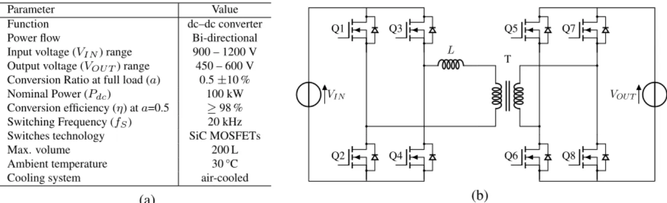
Parameter Value
Function dc–dc converter
Power flow Bi-directional
Input voltage (VIN) range 900 – 1200 V
Output voltage (VOU T) range 450 – 600 V
Conversion Ratio at full load (a) 0.5 ±10 % Nominal Power (Pdc) 100 kW
Conversion efficiency (η) at a=0.5 ≥98 % Switching Frequency (fS) 20 kHz
Switches technology SiC MOSFETs
Max. volume 200 L
Ambient temperature 30 °C
Cooling system air-cooled
(a) VIN VOU T L Q1 Q2 Q3 Q4 Q5 Q6 Q7 Q8 T (b)
Figure 1: (a): List of specifications and arbitrary design choices used as an input to the design process. (b): Circuit diagram of the chosen converter topology: a Dual Active Bridge (DAB). The transformer has an input/output ratio of 2. The input and output capacitors are not depicted here.
An isolated dc–dc converter, the central part of a solid-state transformer (SST, [8]), was chosen as the application case. Such converters have applications in traction [9], wind turbines [10], etc. Here, we focused on a 100 kW, 1200 V/600 V bidirectional, isolated dc–dc converter.
Silicon IGBTs are commonly used as the power switches in this power/voltage range [11]. As recent improvements in SiC technology [12] have resulted in the commercial availability of 1200 V and 1700 V MOSFETs and Schottky Barrier Diodes (SBDs), we focused on SiC power switches in this paper. Indeed, replacing Si IGBTs and diodes with SiC MOSFETs and SBDs in a comparable 100 kW dc–dc converter was shown in [13] to result in a clear improvement in efficiency: 96.9 % at 60 kW max. output power for Si vs 97.9 % at 100 kW max. output power for SiC, while at the same time allowing a much higher switching frequency (20 kHz for SiC and 4 kHz for Si).
The next section briefly introduces the specifications of the converter, and the preliminary design stage which resulted in the selection of the converter topology (as well as some other general design parameters). Section 3 then details the design process all the way up to the physical implementation. The manufacturing and test of the converter are described in Section 4. The design process and its outcome are then discussed in section 5 and a conclusion is given in section 6
2
Pre-design
The specifications of the converter described in this paper are given in Fig. 1a. Some of them are purely functional (input/output voltage, nominal power, target efficiency. . . ), and some are arbitrary de-sign choices (switches technology, switching frequency). These specifications are then used to assess the many dc–dc converter topologies available [10] (Dual Active Bridge – DAB – with or without resonance, resonant converter. . . ). This process of evaluating the topologies is conducted with theoretical analysis and circuit simulations (using ideal components). It is described in more details in [10], and is beyond the scope of this paper. The selection of the most suitable topology is based on the expected efficiency (transformer and power electronics), technical complexity and cost. Regarding the transformer, since its technology and geometry are not yet selected at this stage, the level of each current harmonic is used as a criterion for the losses estimation [14]. For the power electronic switches, conduction and switch-ing losses are estimated based on the datasheets of the SiC dies [15] (on-state resistance and switchswitch-ing energy). The list of possible SiC dies is limited to only two references from Wolfspeed (one 1700 V and one 1200 V-rated MOSFET, along with the corresponding SBDs), because they are the only devices readily available at the time of the pre-design (2014). At this stage of the design, the number of dies to be used per switch position is simply based on their recommended RMS current (as quoted in their datasheet), without any thermal consideration.
As a result of this pre-design stage, a non-resonant DAB topology [16] is selected (Fig. 1b). The leakage inductance L of the Medium Frequency Transformer (MFT) is a key element for the performance of the DAB converter, as it dictates the phase shift between the primary and secondary inverters: if too
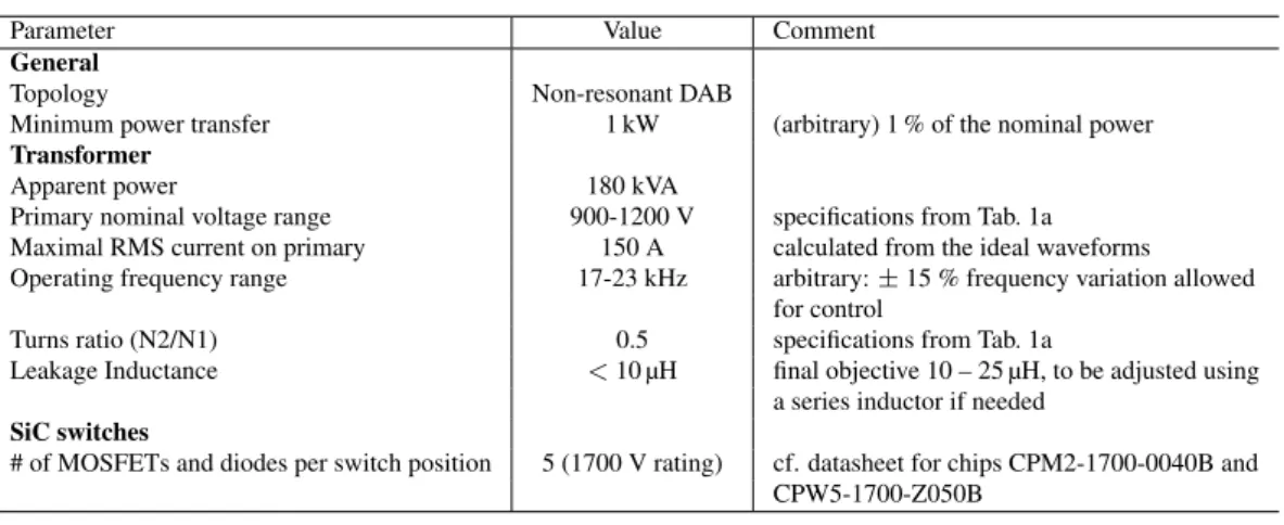
Table I: Outcome of the pre-design stage.
Parameter Value Comment
General
Topology Non-resonant DAB
Minimum power transfer 1 kW (arbitrary) 1 % of the nominal power Transformer
Apparent power 180 kVA
Primary nominal voltage range 900-1200 V specifications from Tab. 1a Maximal RMS current on primary 150 A calculated from the ideal waveforms Operating frequency range 17-23 kHz arbitrary: ± 15 % frequency variation allowed
for control
Turns ratio (N2/N1) 0.5 specifications from Tab. 1a
Leakage Inductance <10 µH final objective 10 – 25 µH, to be adjusted using a series inductor if needed
SiC switches
# of MOSFETs and diodes per switch position 5 (1700 V rating) cf. datasheet for chips CPM2-1700-0040B and CPW5-1700-Z050B
large, this phase shift would limit the transmitted power; if too low, it would make the control too complex [13]. Considering a maximum phase shift range of 10 – 25° (so the power factor is higher than 0.9 in nominal conditions) yields a leakage inductance in the 10 – 25 µH range. Without more information (in particular regarding the control system timing constraints), it is decided to aim for the smallest value; an additional inductor would be connected in series to reach a higher leakage inductance value if needed. This allows to retain some freedom in the design process.
Tab. I presents the main results of the pre-design stage.
3
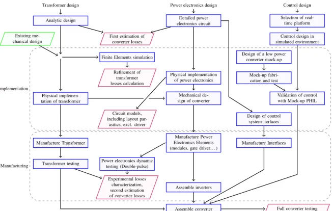
Detailed Design and Implementation
Once the topology and is main parameters have been selected, the detailed design of the converter can begin. As presented in Fig. 2, the design is broken into three main tasks (transformer, power electronics and control), each managed by a different team using the specifications in Fig. 1a and Tab I.
3.1 Transformer design
The details of the transformer design are given in [17]. Because of the short development time, the magnetic material is chosen a priori: among the possible candidates [18], ferrite is selected because of its availability, despite its low maximum induction level (≈ 0.2 T). Amorphous materials are discarded because of their strong magnetostrictive coefficients (risk of acoustic noise); nanocrystalline cores are only available in a limited range of sizes, with long lead times. In particular, 3C90 ferrite material is used because of its suitable performances.
3.1.1 Analytical design
The analytical design allows to quickly compare many configurations, especially regarding copper and core losses. The copper losses in the winding are estimated using Dowell’s equations [19]. These equations consider the current harmonics and estimate the AC resistance of the winding taking into account proximity and skin effects in the conductors [17]. Foil winding is preferred because of its lower cost, lower AC resistance compared to wire, and because it is well suited to the small number of turns being considered here (2 windings with 14 turns per column). The leakage inductance is calculated using [20] at 3.38 µH, a value compatible with the specifications (note that this value does not include the inductance of the connecting cables).
For the core losses, the improved General Steinmetz Equations (iGSE) are used [21]. IGSE requires detailed data regarding the Ferrite material. These data are extracted from the material’s datasheet [22], as we do not have experimental characterization data at this stage.
At the end of the analytical design, it is decided to have the transformer made, because of the long lead time (more than 8 weeks for manufacturing only). The main parameters (number of turns and dimensions of the foils, magnetic material reference) are given to the transformer manufacturer. The mechanical structure (required to hold together the various ferrite parts, the winding and the transformer terminals) is directly proposed by the manufacturer (it is reused from one of their former projects). Many parameters (in particular the location of the terminals of the transformer) are left to the discretion of the manufacturer.
Implementation
Manufacturing
Transformer design Power electronics design Control design Analytic design electronics circuitDetailed power Selection of real-time platform Existing
me-chanical design First estimation ofconverter losses simulated environmentControl design in Finite Elements simulation Design of a low powerconverter mock-up
Refinement of transformer losses calculation
Physical implementation
of power electronics Mock-up fabri-cation and test Physical
implemen-tation of transformer
Mechanical
de-sign of converter Validation of controlwith Mock-up PHIL Circuit models,
including layout par-asitics, excl. driver
Design of control system iterfaces
Manufacture Transformer
Manufacture Power Electronics Elements
(modules, gate driver. . . ) Manufacture Interfaces Transformer testing Power electronics dynamictesting (Double-pulse)
Experimental losses characterization, second estimation of converter losses
Assemble inverters
Assemble converter Full converter testing Figure 2: Flowchart of the detailed design procedure (the corresponding timeline is discussed in the article).
3.1.2 Finite element simulations
While the transformer is being built, Finite Elements (FE) simulations are run. They allow to get a more accurate estimation of the losses (especially for the copper losses). They also allow to perform thermal simulations (temperature distribution over the transformer), electrostatic simulations (to calcu-late parasitic capacitance and check dielectric strength). All calculations are performed using Ansys software: Maxwell for the magnetic and electrostatic simulations, Ansys Mechanical for heat conduc-tion, ICEpak for simulations which mix heat conduction and convection.
The magnetic simulations confirm the leakage inductance value which was calculated analytically (3.38 µH vs. 3.39 µH for FE). They are performed in 3D to represent effects such as current crowding around the power connections. Indeed, these connections are found to represent a large share of the transformer’s ac resistance (up to 60 % [17]). 3D FE offers a much more accurate model of the current distribution in the copper conductors, which unfortunately results in a much greater ac resistance com-pared to the analytical model (Fig. 6a). 3D FE predicts that the ac resistance at 20 kHz is more than twice the dc resistance. At the time of these findings, the transformer is being manufactured, so it is decided to manage the increased losses through additional cooling fans, relying on ICEpak simulations for airflow calculations.
3.2 Power Electronics design
This task refers to the design and implementation of the two inverters of the DAB topology. It also addresses the mechanical structure of the whole converter.
3.2.1 Detailed power electronics circuit
At the time the design is initiated, 1700 V-SiC MOSFETs and Diodes are available on the market as bare dies or discrete, but not in module package [23]. Given the power rating of the converter, a discrete-based circuit is not considered desirable, so we decide to develop a custom power module.
Some simple thermal calculations are performed. First, the switching losses are estimated using the turn-off energy data given in the datasheet of the devices (as we assume Zero-Voltage Switching – ZVS –, turn-on losses are considered negligible). For the conduction losses, the evolution of RDSon with the
temperature is non-negligible (it doubles between 25 and 150 °C for 1700 V MOSFETs), so it is consid-ered in our calculations, assuming an (arbitrary) baseplate temperature of 70 °C and a module thermal
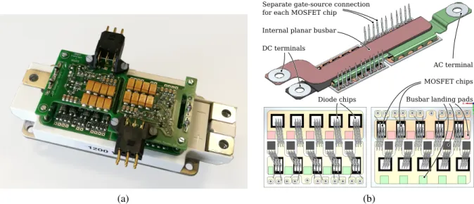
(a)
Separate gate-source connection for each MOSFET chip
DC terminals
AC terminal Internal planar busbar
Diode chips
MOSFET chips Busbar landing pads
(b)
Figure 3: (a) Photograph of the custom power module with the output stage of the gate driver mounted. Length/width of the power module: 152/62 mm. (b) CAD view of the internal interconnects of the power module (top) and layout of the ceramic substrates (where the MOSFETs are located in close proximity with the diode of the opposite switch).
resistance identical to that of the EconoDUAL package from Infineon (which is chosen as the outline for our module). These data confirm that for power modules with 5 MOSFET dies per switch position, the junction temperature remains below the maximum allowed value. On the secondary (600 V side), 1200 V MOSFETs (CPM2-1200-0025B, 25 mΩ RDSon) and diodes (CPW5-1200-Z050B) are used
in-stead of 1700 V devices. This way, the primary and secondary inverters remain geometrically equivalent, and their losses are comparable [24]. An existing gate driver circuit is used here. It was designed for IGBT modules, and is based on discrete components.
Finally, the last elements to be selected are the input/output capacitors. In the absence of any spec-ification regarding input/output ripple voltage, we set it to an arbitrary value of 5 %, and we consider that the input and output capacitors manage the full ac currents of the converter. In the worst case (max-imum voltage – 1200 V – on the primary and the min(max-imum conversion ratio – 0.45) the current values is expected to reach 211 A. Because of the high switching frequency, the required capacitance remains rela-tively low (22 µF). The closest commercially available capacitors are found to be 40 µF capacitors which can sustain 57 A (AVX FFVS6U0406K). 4 such capacitors are then connected in parallel to provide suf-ficient current capability, and much higher capacitance value than initially required. For modularity and cost aspects, the same capacitors are used for the primary and secondary sides.
At this stage, by combining the estimation of losses from the power semiconductor devices and from the transformer (as calculated using the analytical model), we reach a first milestone where the efficiency of the converter (“first estimate” line, in Fig. 8b) can be compared to the target efficiency in the specifications (98 %, see Fig. 1a)
3.2.2 Physical implementation of the power electronics
At this point, the detailed circuit diagram of the converter has been drawn, and the exact references of all components are known. The most specific components (SiC MOSFETs and diodes, capacitors) are ordered, as they have relatively long lead times (more than 8 weeks).
As mentioned above, a custom power module is designed with the ”EconoDUAL” outline (Fig. 3a). Although the SiC MOSFETs have an internal body diode, we are not sure we can use it reliably. As a consequence, we decide to use antiparallel SiC SBDs. To satisfy the current ratings of the diodes, 5 chips are used per switch position (i.e our module contains as many diodes as MOSFETs). This is probably far from optimal, but reflects the lacks of reliability data at the time the decision is taken (end 2014). Regarding the internal routing of the power module, various configurations are compared with regard to their parasitic inductances. The models are first designed with a 3D mechanical CAD software (CREO
Transformer
Power modules Busbar
Heatsinks
Gate drive boards in position Aluminium frame (a) 0 100 200 300 400 time [ns] −500 0 500 1000 1500 VDS [V ] ID VD dI dt=−10 kA/µs ∆V = 680 V −100 0 100 200 300 ID [A ] (b)
Figure 4: (a): CAD view of the complete converter (without cables). (b): Time-domain simulation result for the turn-off (V = 1000 V ; I = 300 A ; di/dt = -10 kA/us), including the modelling of the interconnects (especially the inductive behaviour), in a double-pulse configuration (hard switching).
Parametric, Fig. 3b), then the parasitic inductances are calculated using Ansys Q3D Extractor. The gate and source connections of each die are routed independently, to keep some flexibility in case issues are encountered in the parallel operation of the MOSFETs: all transistors can be connected in parallel, or they can be driven through individual gate resistors, depending on the layout of the gate driver board. In our case, 5 Ω resistors are connected between the output stage of the gate driver and each gate terminal of the power module .
3.2.3 Mechanical design of converter
Based on the thermal calculations performed previously, plus some safety margins (we consider each module dissipates 500 W, has a baseplate temperature of 70 °C and shall operate at a maximum junction temperature of 120 °C so as not to degrade its RDSon too much), we select an aluminium heatsink with
embedded copper heatpipes for better heat spreading (Mersen, 205×300×120 mm3), with three 92 mm axial fans (Papst). This heatsink is used as the support to mount all the components of each inverter. A 3D implementation of the inverters is done using mechanical CAD software, with a custom laminated busbar used to connect the power modules. Inverters and transformer are then secured to an aluminium frame (Fig. 4a).
3.2.4 Circuit models
Electromagnetic simulations are performed using the Ansys Electromagnetic suite [25]: parasitic inductances, capacitances and resistances are calculated (using Q3D Extractor) from the 3D geometry of the inverters. An equivalent circuit model is automatically generated, and included in a time-domain simulation (Simplorer). As no models are available for the MOSFETs, we use the simplified macro model proposed in [26]. However, even this simplified model is found to be too complex for the converter simulation to run in a reasonable time (we have 20 dies per power module, and 4 power modules total). Finally, we end up using ideal switch and diode models with capacitors in parallel. These capacitors are important as, together with the inductors in the circuit, they set the switching transients. Fig. 4b presents a simulation result during turn-off.
From the simulated voltage and current waveforms (Fig. 4b), the global parasitic inductance of the commutation loop (capacitor, busbar and power module.) is evaluated at 68 nH [27]. Finally, more detailed electromagnetic simulations are performed using Ansys Maxwell to analyze the current density distribution in the interconnects (wirebonds, busbar. . . ). However, these cannot be conducted using the complex current waveforms produced by the circuit simulation, and must be limited to dc. This limits their relevance (skin and proximity effects are not taken into account in the resulting current distribution As no obvious issue is identified through the simulation, the design stage is considered finished for the power electronics, and manufacturing can start.
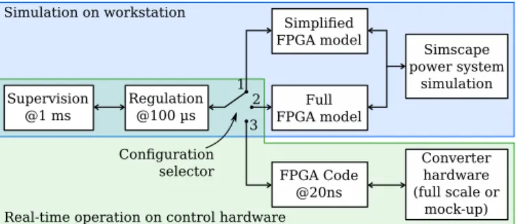
Supervision @1 ms Regulation@100 µs Simscape power system simulation Converter hardware (full scale or mock-up) Simplified FPGA model Full FPGA model FPGA Code @20ns 1 2 3 Configuration selector Simulation on workstation
Real-time operation on control hardware
Figure 5: Architecture of the control. Conf. 1 is used for high level simulations. Conf. 2 simulates the operation of the FPGA, so it is complex and only short periods of time can be simulated (100 ms max.). Conf. 3 runs on the RCP platform connected to converter hardware in real-time (the indicated times correspond to the recurrence period of each task).
3.3 Control design
The control hardware solutions can be divided into three families: completely custom boards, de-velopment boards, and rapid control prototyping (RCP) platforms. RCPs provide very advanced code generation and debugging capabilities, but come at a cost of several tens of thousands of euros (for the hardware and the software licences). This is considered the most suitable solution in our case, because of the short development time. Many RCPs are available on the market. We select a system from Speed-goat [28] because of its modularity, good integration with the Matlab/Simulink coding platform, and cost. This system includes a x86 Intel processor for all the calculation-intensive, low frequency tasks and a Spartan 6 Xilinx FPGA for the high frequency tasks such as the generation of the firing signals, the management of the error signals from the converter, and the acquisition of the measurements.
The control system architecture is depicted in Fig. 5. It is designed using Simulink, with three configurations. The first two are used for simulation (the code is run on a workstation, completely off-line), while the third is the Power Hardware-In-the-Loop (PHIL) configuration, where the code is implemented in the real-time hardware and actually controls the converter. This ensures that the same code is used for the simulation and the actual control [24].
In parallel, a “small scale mock-up” converter is assembled. It simply consists in a low voltage (50 V), low power (100 W) DAB converter built on a “breadboard”-type prototyping board. This small-scale mock-up is connected to the Speedgoat system. The mock-up has a low fidelity to the actual converter (in particular, its transformer, being an off-the-shelf item, has very different leakage and mag-netizing inductances), so it cannot be used to fully validate the control algorithm. It is useful, however, to detect issues associated with the real-time operation. Indeed, a very detailed simulation of the control system including the internal operation of the FPGA (configuration 2 in Fig. 5) is possible but very slow. Practically, it is not possible to simulate more than a 100 ms of operation. Therefore, any issue that would occur over longer periods (such as a timer overflow, for example), would go unnoticed in simu-lation. This is where the PHIL operation, using the actual control hardware and the mock-up converter becomes useful: it runs in real-time, over much longer periods (minutes or hours), and in the worst case, a dramatic failure only involves a moderate amount of energy (compared to the full scale DAB).
4
Manufacturing and experimental Validation
This section describes the “Manufacturing” part of Fig. 2 (the dashed box at the bottom), as well as the evaluation tests performed on individual elements, and finally on the converter.
4.1 Transformer testing
Once the transformer built, it is characterized using an inverter available at Laboratoire Amp`ere: short-circuit test (which allows the measurements of the copper losses in the winding) and open circuit test (for the measurement of the core losses). All measurements are performed at the nominal frequency (20 kHz). The resistance increase with frequency is measured using an impedance analyzer (Keysight E4990A).
102 103 104 105 Frequency [Hz] 1 10 FR = RAC RDC Measurement Dowell 3D FE simulation (a) 2:1 i1 i2 A R1 9.5 mΩ Lf 4.4 µH B C1 3 nF Lm 5.5 mH R2 1.4 mΩ C2 10 nF C D C122.8 nF v1 v2 (b)
Figure 6: (a):Evolution of the ac resistance (relative to the dc resistance), as forecast by various analytical models, by FEM simulation, and as measured. (b): Equivalent model of the medium frequency transformer identified from measurements. (a) 200 400 time [ns] 0 500 1000 1500 VDS 200 400 600 time [ns] ID VD 0 100 200 300 ID (b)
Figure 7: (a) dc connections used for double-pulse tests on the power module, including a film capacitor, a custom busbar made out of printed circuit board, and a high bandwidth Rogowski-coil current sensor (Fraunhofer IZM). (b): corresponding waveforms measured on the power modules, used to refine the losses model and to adjust the output impedance of the gate driver. Note that the interconnects used here are different from the complete busbar used for the simulations in Fig. 4b, hence the different over-voltage.
losses, especially as the frequency increases. It also confirms that the 3DFE modelling offers as satisfying level of precision. An analysis of these differences is available in [17].
In order to check the interactions between the transformer and the other components (switches, bus-bar. . . ), an equivalent model of the transformer is required. The circuit diagram of this equivalent model is depicted in Fig. 6b, after identification with the measurements.
4.2 Power electronics dynamic testing
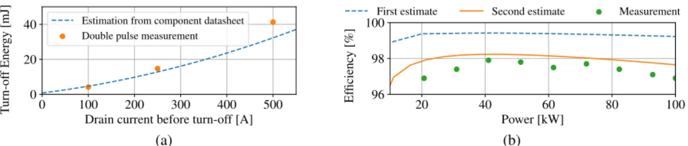
The power modules are manufactured first (DeepConcept, Tarbes, France). They are characterized using a double pulse test circuit (Fig. 7a, principle described in [26]), which allows the measurements of the hard-switching losses. An example of measured waveforms is given in Fig. 7b. Thanks to such measurements, we can adjust the switching energy losses (turn-off losses only, as turn-on losses occur under zero voltage switching conditions) used in our estimation. As it can be seen in Fig. 8a, the use of the coefficients calculated from the datasheet of the dies causes an underestimation of the turn-off energy loss of up to 15–20 %. Together with the experimental characterization of the transformer, these results are used to produce the “second estimate” line in Fig. 8b. The double-pulse test circuit is also used to adjust the output impedance of the gate driver (a small capacitor is added to increase the gate-to-source capacitance of the MOSFETs). In parallel, the complete converter is assembled according to the CAD plans. The result is visible in Fig. 9a.
4.3 Full converter testing
Once the test bench has been set-up (a time-consuming task for a converter this size), the actual test-ing of the power converter is relatively straightforward: the control system is connected to the converter,
0 100 200 300 400 500 Drain current before turn-off [A] 0 20 40 Turn-of fEner gy
[mJ] Estimation from component datasheet
Double pulse measurement
(a) 20 40 60 80 100 Power [kW] 96 98 100 Ef ficienc y [%]
First estimate Second estimate Measurement
(b)
Figure 8: (a): Comparison between the switching losses estimated from the manufacturer’s datasheet and from the double-pulse test, for 5 1700 V-SiC MOSFETs and a dc voltage of 1200 V. (b): comparison between the global efficiency as forecast initially, after refinement of the design and the models, and eventually measured.
(a) 0 2 4 time [µs] −1000 −500 0 500 1000 V [V] ID V1 V2 24 26 28 time [µs] −200 −100 0 100 200 I[A] (b)
Figure 9: (a): Photograph of the final converter. Total dimensions are 43×46×71 cm3(140 L). (b): Waveforms
measured on the converter in operation
and power is gradually increased. A waveform measured at the output of the primary inverter during operation is shown in Fig. 9b. Efficiency measurements are presented in Fig. 8b. The final efficiency is slightly below that predicted by the design, even after the second round of estimation. Note, however, that this efficiency measurement is performed with the voltage/current sensors used for the control of the converter, and therefore has a limited accuracy.
While the converter works, with an efficiency reaching almost 98% (the objective in Fig. 1a) over a large part of the power range, some issues must be highlighted (and will be discussed in the next section): • EMC issues are encountered, causing a malfunction of the control system (the internal FPGA is reset by EMI above 50 kW). This is solved by re-routing the cables of the test bench (many were overlapping), by adding ferrite beads on auxiliary power supplies and driving signal cables, and by providing earth connection of all metal screen on one point only. The control software is also made more robust to EMI transients by filtering outliers from the I/Os.
• At 1200 V, two power modules are found to fail, because of arcing between the internal busbars (the black and red metal sheets in Fig. 3b). This is attributed to an insufficient clearance between the parts, and possibly to a bubble in the silicone encapsulant. The other modules do not seem to be affected.
5
Discussion
A 100 kW converter was entirely designed and built over the course of one year. Its final performance, although not fully in line with the specifications (the efficiency, in particular, is slightly below 98%), are remarkably close. The converter can operate continuously, indicating that the thermal management system is able to absorb the higher losses level.
As explained in the introduction, the objective of this article is to reflect upon the design process. As the converter was essentially “built from scratch”, the design was not based on incremental improvements of an existing converter. This means that in many cases, questions were asked in absolute terms (will it work?) rather than in relative terms (will it work better?). This is an essential difference, in particular for computer simulation, as in the “absolute” case, no reference data are available. Therefore, the accuracy of the modelling is unknown at the design stage.
When looking back on the design process, summarized in Fig. 2, one striking fact emerges: despite the effort which was put in the modelling and simulation, almost none of the simulation results were actually fed back in the process: in Fig. 2, simulation results are outputs (red boxes), mere “milestones” used to check that the converter meets its specifications. In no occasion did the simulation results led to changes in the design, which was finally mainly based on simple analytical approaches and on the datasheets of the components. However, this observation masks fundamental differences between mod-els, which we will discuss now.
For the transformer design, the numerical modeling is found to be remarkably accurate, capable to identify issues such as an increase in ac resistance caused by the geometry of the terminals. 3D FE simulations are not simply a refinement of the analytical calculations: they offer a very different picture, which may have resulted in changes in the design of the transformer, had we not sent it to manufacturing beforehand. The main issue here is that simulations take time: one week for the electromagnetic calcula-tions, not including the preparation of the model, the analysis of the results, and the subsequent thermal simulations. It is, however, a worthwhile effort, and the simulation time could be reduced by using more powerful computing hardware.
Regarding the design of the control system, the RCP provides a very efficient way to (almost) seam-lessly transfer from a block-diagram description to real-time code. An intermediary test using a small-scale mock-up remains valuable, as it helps capturing issues which might not be detected in simulation (typically the overflow of a register which occurs over a long period). This is especially important, as the debugging capabilities are limited for the FPGA circuit. All designs we currently work on include such small-scale mock-up stage, with three major improvements: the mock-ups are now made on PCBs (as opposed to breadboard, which was found not to be reliable enough), they now use exactly the same inter-face as the final converter, and are designed to have the same dynamics, so the transfer to the full-scale converter is even more straightforward.
The power electronics simulations present a completely different picture: over the course of the project, we have never been able to perform a complete circuit simulation of the converter (i.e includ-ing accurate models of the switches, their gate drive circuits, as well as the circuit parasitics and the transformer model). This level of complexity is too demanding for the circuit simulator. Ideal switches (on/off behaviour) with a linear capacitor in parallel were used as a model for the SiC MOSFETs instead. A second (and related issue) is that SiC MOSFETs models are not available for all simulation platforms (Wolfspeed provides SPICE models, and we use Ansys Simplorer). This required the adjustment of a compatible model using a dedicated tool (in Simplorer) and the datasheet of the MOSFET. Generating a model this way is convenient, but does not give any information about its level of accuracy, or about its domain of validity.
Even if we had been able to simulate the power circuit of the converter, this would probably have been insufficient to predict the EMC issues we encountered during the tests (spurious resets of the control systems above a certain power level). This would have required to take into consideration the entire converter, including models of the gate drivers, the auxiliary power supplies, the low power wiring, the grounding configuration, etc. Not only would such approach require tremendous computing power, but it would also require models for these elements. Another approach could be to perform model reduction, to adapt the models to the analyses (i.e. to use a different model to predict EMI or power losses). This,
however, requires considerable expertise, time, and data. Some of these data being not available, it requires experimental characterization, and therefore advance purchase of some elements [29]. Finally, for subsequent designs, we use a more protective approach regarding EMC, for example using fiber optics as a link between the control system and the converter (for driving signals as well as for measurements). While it provides an ideal barrier to EMI, it comes at a certain cost.
As for the other issue encountered (arcing inside one power module), preventing it through simula-tion, if possible at all, would have required a totally different modelling. It is not clear yet if the issue was related to thermo-mechanical effects (deformation of the internal leadframe as a consequence of heating), manufacturing issues (inaccuracy in the forming of the metal parts, in their alignment, bubble in the silicone encapsulant), design issue (insufficient clearance between the parts), or (more probably) a combination of the three. The multiplicity of the possible causes makes modelling quite complicated, and one can consider that hardware prototyping is unavoidable here. This is, however, a specific case: custom modules were required as no 1700 V SiC power modules were available at the time. With “off-the-shelf” modules, any such design issue would have been addressed beforehand by the manufacturer.
6
Conclusion
A 100 kW converter was designed “from scratch”, over a relatively short time-frame (1 year from beginning of design to test), with the objective of assessing the design methodology. The design process was separated between three main elements: transformer, power electronics, and control system.
Thanks to RCP techniques, which rely on seamless transition from computer model to firmware generation, the control was developed independently from the transformer and the converter. This is not so true for hardware elements such as the transformer and the power electronic circuits, for which computer simulation was found to be less straightforward.
For the transformer, 3D-FE simulation was found to be accurate, but requires a lot of effort and time to set the model up, run the simulation, and analyze the results. However, it is worth the effort, and new transformer designs we have made since have relied heavily on 3D-FE simulation.
For the power electronics, on the contrary, no complete simulation could be run, because of the complexity of the model. Simplifications were required which, together with un-verified models for the semiconductor devices, produced simulation results of unknown validity. As a consequence, the power electronics design was mainly based on datasheet information, safety margin, or designer expertise.
More importantly, the lack of complete circuit simulation did not allow us to identify EMC issues, which required fixing the converter on the test bench. Here, the solutions rely more on EMI-safe ap-proaches (such as fiber optics data transfer) than on computer simulation.
This does not mean that simulation is useless. For incremental changes (e.g. improving a prototype before moving to production), a reference is available to check the validity of the models. In this case, simulation gives an invaluable analysis tool. Simulation is also quite useful for optimization or to evaluate the consequences of changing a design parameter. But in the case of a relatively large converter such as the one presented here, electrical simulation does not currently allow the generation of a complete “virtual prototype” which could replace a hardware prototype.
References
[1] J. W. Kolar, J. Biela, T. Friedli, and U. Badstuebner, “Performance trends and limitations of power electronic systems,” in Proceedings of the Conference on Integrated Power Systems (CIPS), 2010.
[2] D. Bortis, D. Neumayr, and J. W. Kolar, “ηρ-Pareto Optimization and Comparative Evaluation of Inverter Concepts considered for the GOOGLE Little Box Challenge,” in Proceedings of the 17th IEEE Workshop on Control and Modeling for Power Electronics (COMPEL 2016), 2016, p. 11 p.
[3] C. Marxgut, J. Muhlethaler, F. Krismer, and J. W. Kolar, “Multiobjective optimization of ultraflat magnetic components with pcb-integrated core,” IEEE Transactions on Power Electronics, vol. 28, no. 7, pp. 3591–3602, 2013.
[4] P. Solomalala, J. Saiz, A. Lafosse, M. Mermet-Guyennet, A. Castellazzi, X. Chauffieur, and J.-P. Fredin, “Multi-domain simulation platform for virtual prototyping of integrated power systems.” in Power Electronics and Applications, 2007 European Conference on, Sep. 2007, pp. 1–10.
[5] J. Biela, J. Kolar, A. Stupar, U. Drofenik, and A. Muesing, “Towards Virtual Prototyping and Comprehensive Multi-Objective Optimisation in Power Electronics,” in Power Conversion and Intelligent Motion Conference (PCIM 2010), Nuremberg, Germany, May 2010, p. 23.
[6] P. L. Evans, A. Castellazzi, and C. M. Johnson, “Automated fast extraction of compact thermal models for power electronic modules,” IEEE transactions on power electronics, vol. 28, no. 10, pp. 4791–4802, 10 2013.
[7] F. Pˆecheux, C. Lallement, and A. Vachoux, “Vhdl-ams and verilog-ams as alternative hardware description languages for efficient modeling of multidiscipline systems,” IEEE transactions on Computer-Aided design of integrated Circuits and Systems, vol. 24, no. 2, pp. 204–225, 2005.
[8] J. E. Huber and J. W. Kolar, “Solid-state transformers – on the origins and evolution of key concepts,” IEEE Industrial Electronics Magazine, 2016.
[9] C. Zhao, A. Dujic, Drazenand Mester, J. K. Steinke, M. Weiss, S. Lewdeni-Schmid, T. Chaudhuri, and P. Stefanutti, “Power Electronic Traction Transformer–Medium Voltage Prototype,” IEEE transactions on Power Electronics, vol. 61, no. 7, pp. 3257–3268, Jul. 2014.
[10] T. Lagier and P. Ladoux, “A comparison of insulated DC-DC converters for HVDC off-shore wind farms,” in 2015 International Conference on Clean Electrical Power (ICCEP), June 2015, pp. 33–39.
[11] S. Bernet, “Recent developments of high power converters for industry and traction applications,” IEEE Transactions on Power Electronics, vol. 15, no. 6, pp. 1102–1117, nov 2000.
[12] J. Mill´an, P. Godignon, X. Perpi˜n`a, A. P´erez-Tom´as, and J. Rebollo, “A Survey of Wide Bandgap Power Semiconductor Devices,” IEEE transactions on Power Electronics, vol. 29, no. 5, pp. 2155–2163, May 2014.
[13] H. Akagi, T. Yamagishi, N. M. L. Tan, S. i. Kinouchi, Y. Miyazaki, and M. Koyama, “Power-loss breakdown of a 750-v 100-kw 20-khz bidirectional isolated dc – dc con750-verter using sic-mosfet/sbd dual modules,” IEEE Transactions on Industry Applications, vol. 51, no. 1, pp. 420–428, Jan 2015.
[14] A. Perreira, “Conception de transformateurs moyennes fr´equences : application aux convertisseurs dc-dc haute tension et forte puissance,” Ph.D. dissertation, Universit´e Lyon 1, 2016.
[15] T. Lagier, P. Ladoux, and P. Dworakowski, “Potential of silicon carbide MOSFETs in the DC/DC converters for future HVDC offshore wind farms,” High Voltage, vol. 2, no. 4, pp. 233–243, 2017.
[16] R. W. DeDoncker, M. H. Kheraluwala, and D. M. Divan, “Power conversion apparatus for dc/dc conversion using dual active bridges,” Patent US Patent 5,027,264, Jun. 25, 1991, US Patent 5,027,264.
[17] A. Pereira, B. Lefebvre, F. Sixdenier, M.-A. Raulet, and N. Burais, “Comparison Between Numerical and Analytical Methods of AC Resistance Evaluation for Medium Frequency Transformers: Validation on a Prototype,” in Electrical Power and Energy Conference (EPEC), 2015 IEEE, ser. Electrical Power and Energy Conference (EPEC), 2015 IEEE, London, Canada, Oct. 2015. [Online]. Available: https://hal.archives-ouvertes.fr/hal-01374145
[18] R. Hilzinger and W. Rodewald, Magnetic Materials. Erlangen: Publicis, 2013.
[19] P. Dowell, “Effects of eddy currents in transformer windings,” in Proceedings of the Institution of Electrical Engineers, vol. 113, no. 8. IET, 1966, pp. 1387–1394.
[20] B. Cougo and J. W. Kolar, “Integration of leakage inductance in tape wound core transformers for dual active bridge converters,” in Integrated Power Electronics Systems (CIPS), 2012 7th International Conference on. IEEE, 2012, pp. 1–6.
[21] K. Venkatachalam, C. R. Sullivan, T. Abdallah, and H. Tacca, “Accurate prediction of ferrite core loss with nonsinu-soidal waveforms using only steinmetz parameters,” in Computers in Power Electronics, 2002. Proceedings. 2002 IEEE Workshop on. IEEE, 2002, pp. 36–41.
[22] Ferroxcube, Datasheet – 3C90 Material Specifications, 2008. [Online]. Available: https://www.ferroxcube.com/upload/ media/product/file/MDS/3c90.pdf
[23] CREE. (2014, sep) Cree introduces industry’s first 1.7-kv, all-sic power module. [Online]. Available: http: //www.cree.com/news-media/news/article/cree-introduces-industry-s-first-1-7-kv-all-sic-power-module
[24] T. Lagier, L. Ch´edot, F. Wallart, L. Ghossein, B. Lefebvre, P. Dworakowski, M. Mermet-Guyennet, and C. Buttay, “A 100 kW 1.2 kV 20 kHz, DC-DC converter prototype based on the Dual Active Bridge topology,” in 19th International Conference on Industrial Technology (ICIT 2018), 2018.
[25] Ansys, ANSYS Electronics Desktop (online), 2017. [Online]. Available: http://www.ansys.com/products/electronics/ ansys-electronics-desktop
[26] J. Fabre, P. Ladoux, and M. Piton, “Characterization and implementation of dual-sic mosfet modules for future use in traction converters,” IEEE Transactions on Power Electronics, vol. 30, no. 8, pp. 4079–4090, 2015.
[27] J. Wang, H. S.-h. Chung, and R. T.-h. Li, “Characterization and experimental assessment of the effects of parasitic elements on the mosfet switching performance,” IEEE Transactions on Power Electronics, vol. 28, no. 1, pp. 573–590, 2013.
[28] P. Dworakowski, L. Chedot, and F. Wallart, “Supergrid institute – an efficient and compact power converter to enable the supergrids of the future,” Speedgoat User Stories, Tech. Rep., 2016. [Online]. Available: https://www.speedgoat.com/user-stories/speedgoat-user-stories/supergrid-institute
[29] M. Foissac, J. Schanen, G. Frantz, D. Frey, and C. Vollaire, “System simulation for emc network analysis,” in Applied Power Electronics Conference and Exposition (APEC), 2011 Twenty-Sixth Annual IEEE. Fort Worth, USA: IEEE, mar 2011, pp. 457–462.