The effect of periodic silane burst on the properties
of GaN on Si (111) substrates
Zang Keyan1, Chua Soo Jin1, Carl V. Thompson1,2
1 Singapore-MIT Alliance, E4-04-10, NUS, 4 Engineering Drive 3, Singapore 117576 2 Department of Materials Science and Engineering, MIT, Cambridge, Massachusetts 02139
Abstract
—
The periodic silane burst technique was employedduring metalorganic chemical vapor deposition of epitaxial GaN on AlN buffer layers grown on Si (111). Periodic silicon delta doping during growth of both the AlN and GaN layers led to growth of GaN films with decreased tensile stresses and decreased threading dislocation densities, as well as films with improved quality as indicated by x-ray diffraction, micro-Raman spectroscopy, atomic force microscopy, and transmission electron microscopy. The possible mechanism of the reduction of tensile stress and the dislocation density is discussed in the paper.
Index Terms— Metal-organic Chemical Vapour Deposition, III-V Nitrides
I.
eteroepitaxial growth of Gallium nitride (GaN) materials has been intensively studied for the application in opto-electronic devices and high-power, high temperature microelectronic devices due to its wide bandgap characterics. Major developments have led to the commercial products such as high brightness blue/green light emitting diodes
INTRODUCTION
1
and laser diodes 2. Growth of GaN onto silicon substrate offers very attractive potential for incorporating GaN devices onto silicon-based very large-scale integrated circuits, low cost and available in large wafer size of silicon. However, due to the large difference in lattice constant, crystal structure, and thermal expansion coefficient, it is rather difficult to epitaxially grow GaN on Si substrate3. A high density of threading dislocations on the order of (109~1010 cm-2) exists in the GaN film on silicon substrates due to large lattice mismatch, which will affect the performance of the GaN based devices4-6. On the other hand, cracks are typically formed either due to the large tensile stress in the GaN film during growth or during the cooling down process with large difference in thermal expansion coefficient between GaN and Si. Reducing tensile stress and dislocation density are the important issues to be solved for the growth of crack-free and device-quality GaN on silicon substrate. To overcome these difficulties, many solutions including introduction of low temperature-AlN interlayer7-9, SiNx mask10 or delta-doping
technique11-13 during the growth of GaN layer have been attempted as an effective way to reduce the dislocation densities and improve the crystalline qualities of GaN films on silicon.
In this study, we report the growth of high quality of GaN on silicon with periodic silane burst during growth of both the high-temperate AlN buffer layer and GaN layers by metalorganic chemical vapour deposition (MOCVD). The effects of the periodic silane burst technique on the reduction of dislocation density and tensile stress are studied by atomic force microscopy (AFM), X-ray diffraction (XRD) and micro-Raman. The cross-sectional and plane-view transmission electron microscopy (TEM) was carried out to study its effect on the crystal quality of GaN film.
II. EXPERIMENTAL DETAILS
MOCVD growth of GaN on Si (111) substrates was performed in an EMCORE-D125 system. Trimethylgallium (TMG), trimethylaluminium (TMAl), ammonia and dilute silane were used as source materials for Ga, Al and Si, respectively. Hydrogen was used as carrier gas. The Si (111) substrate was cleaned using the RCA recipe followed by dipping in HF solution to form a hydrogen-terminated surface. The substrate was initially annealed in an H2
ambient at 1020ºC for 15 min to remove the native oxide. A 100 nm AlN was epitaxially grown as the buffer layer at 1020 oC, followed by the deposition of 1.2µm GaN at 1010
o
C. The flow rate of TMG and ammonia is kept at 150µmol/min and 0.45mol/min, respectively. The chamber pressure was maintained at 200Torr. Silane burst was inserted into the layers through a silane flow of 0.167µm/min for 36 seconds during periodic growth interruption with ammonia on. There are 13 periods of silane bursts in AlN layer and 5 periods in GaN layer. Sample without silane bursts was grown under the same condition for the comparison experiment.
The surface morphology of GaN was characterized using a Digital Instruments Nanoscope III AFM set up under tapping mode. The cross-sectional and plane-view TEM analyses were carried out using a Philip EM 300 TEM. The structural properties of GaN were characterized using X-ray diffraction and JY-T64000 Micro-Raman under the z(x_)
z
backscattering configuration with the scattering light parallel to the c axis of GaN films. The accuracy during the Raman measurements was 0.2cm-1 with a lateral spatial resolution of 1.0µm.III. RESULTS AND DISCUSSION
The surface morphology of the GaN film with and without silane burst is shown in Fig. 1. Without silane burst, there are ‘void’ defects terminated at the surface steps, which can be associated with the open core dislocations with the screw type components. The root mean square (RMS) roughness of sample without silane burst is 0.9nm in a 2µm×2µm area, and the dislocation density is 2.1×1010 cm-2. While with silane burst, much better surface morphology is obtained. The steps and terraces are clearly seen in Fig. 1b and they are most likely related to the termination of the mixed dislocations at the GaN surface. There are also a number of pure edge dislocations terminating on the free surface without accompanying steps as dislocation pits (indicated as arrows). The density of dislocations at surface is estimated about 6.7 × 109 cm-2 by counting the number of pits. The RMS roughness is improved to 0.4nm. The surface morphology of GaN with silane burst is comparable to conventional GaN grown on sapphire substrate. Thus periodic silane burst is believed to improve the surface morphology and decrease the density of the dislocations.
FIG. 1. Tapping mode AFM images of GaN films (a) as-grown layer without periodic silane burst and (b) as-as-grown layer with periodic silane burst.
The XRD results of the rocking curves (ω scan) of (0002) GaN symmetric plane and (10
1
2) asymmetric plane are shown in Fig. 2a and Fig. 2b respectively. The full width at half maximum (FWHM) values of ω scan is largely reduced with inserting periodic silane burst. The rocking curves of symmetric plane shows the mosaic distribution in the GaN films, and normally sensitive to the screw and mixed types of threading dislocations. However, the rocking curve of the (101
2) asymmetric plane can shows the effect of all types of threading dislocations, including edge dislocations. Therefore, from the narrowing of the rocking curve of (0002) peak, we can know that the crystal quality is improved and threading dislocations are reduced by inserting the periodic silane bursts.-0.5 0.0 0.5
(a)
without silane burst with silane burst
N o rm a li z e d In te n s it y ( a .u .) Normalized ω (o) -0.5 0.0 0.5 (b) N o rm a liz e d I n te n s it y (a .u .) Normalized ω(o) withsilane burst without silane burst
FIG. 2. XRD spectra of GaN films without (dash line) and with (solid line) periodic silane burst technique. (a) High Resolution XRD rocking curve around (0002) reflection. (b) High resolution XRD rocking curve around (10
1
2
) reflection.Raman spectra from crack-fee regions of GaN films are shown in Fig. 3. The spectra show strong E2(TO)-high and
A1(LO) modes under z(x_)
z
scattering geometry. TheE2(TO) phonon peaks are of 563.7cm-1 and 565.7cm-1 for
sample without and with silane burst respectively. A1(LO)
peak position is at 730.9cm-1 and 732.7cm-1 for sample without and with silane burst respectively. The phonon frequency from both sample show blue shift with respect to Raman peaks of stress-free GaN. The E2(TO) phonon peak
of a 400µm thick free-standing strain free GaN was measured at 567.5cm-1. Since the E2(TO) phonon frequency
is sensitive to strain, it has been extensively used to estimate the in-plane stress. The blue shift of E2 phonon
indicates the tensile stress in the GaN films. The sample without silane burst shows larger E2 phonon shift, which
means larger biaxial tensile stress in the GaN film. Using the established relationship between biaxial stress and E2
phonon shift in GaN/Si (111) derived by our group 14 the biaxial tensile stress in GaN films can be calculated: 0.88GPa for sample without silane burst, and 0.42GPa for sample with silane burst. It is pointed out that the Raman spectrum is measured at the crack-free region. For the sample with silane burst, there are very few cracks on the surfaces. This result suggests that the periodic silane burst
largely reduce the tensile stress in the GaN films. Due to large lattice mismatch between GaN and Si, GaN undergoes a large tensile stress at growth temperature. Periodic silane burst produces a method for the reduction of this tensile stress. 550 600 650 700 750 800 λ exc=514.5nm A1(LO) E2H In te n s ity (a rb . un it s ) Raman Shift (cm-1)
FIG. 3. Raman spectra of GaN films without (dash line) and with (solid line) periodic silane burst. The spectra resolution is 0.2cm-1.
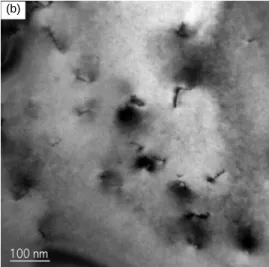
The cross-sectional bright-field TEM (shown in Fig. 4) are carried out to study the effect of silane burst on the microstructure of the GaN films. The GaN sample without silane burst presents a large number of threading dislocations (~1010 cm-2) readily propagate from the interface of GaN and AlN buffer layer to the surface. However, the density of threading dislocations is largely reduced in Fig. 4b for the sample with silane burst. These observations are confirmed by plan-view TEM (shown as Fig. 5). The dislocation density of sample with silane burst estimated from plan-view TEM image is 5×109cm-2, which is consistent with the AFM result. Sample without silane burst reveals a high density of dislocations in the range of 1010cm-2. It is noticed that some of the threading dislocations are observed to terminate inside the film. This termination of the threading dislocations is a result of periodic silane burst in the GaN film. Since there is a large stress field around the dislocation cores and the impurities such as Si are easily trapped in the tensile stress region. Therefore, the Si-based impurities (complex) or SiNx would
prefer to decorate around the dislocation core due to the sufficiently large tensile stress field when silane is introduced into the chamber with ammonia. By doing so, the propagation of threading edge dislocation20 to the film surface is most likely terminated at the Si-based (complex) or SiNx. And also, the tensile stress can be relatively
relaxed by the decoration of the impurities at the dislocation cores. (a) GaN 550 555 560 565 570 575 580 E2H without with AlN
FIG. 4. The cross-sectional TEM images of samples without (a) and with (b) silane burst. The image was taken in <11
2
0> direction. Si 100nm (b) GaN AlN Si 200nm (a)FIG. 5. The plan-view TEM of GaN samples without (a) and with (b) periodic silane burst
IV CONCLUSION
We have demonstrated that periodic silane burst improve the crystal quality of GaN films grown on Si (111) substrates by MOCVD. The periodic silane burst is an effective way to reduce the propagation of the threading dislocations, and also reduce the biaxial tensile stress in the GaN films.
REFERENCES
[1] S. Nakamura, M. Senoh, S. Nagahama, N. Iwasa, T. Yamada, T. Matsushita, Y. Sugimoto, and H. Kiyoku, Jpn. J. Appl. Phys. 36, L1059 (1997).
[2] S. Nakamura, M. Senoh, S. Nagahama, N. Iwasa, T. Yamada, T. Mat-sushita, H. Kiyoku, Y. Sugimoto, T. Kozaki, H. Umemoto, M. Sano, and K. Chocho, Jpn. J. Appl. Phys. 36, L1568 (1997)
[3] A. Krost and A. Dadgar, Mater. Sci. Eng. B93, 77 (2002) [4] S. Nakamura, Science 281, 956 (1998)
[5] S. Sasaoka, H. Sunakawa, A. Kimura, M. Nido, A. Usui and A. Sakai, J. Cryst. Growth 189/190, 61 (1998)
[6] A. Osinsky, S. Gangopadhyay, r. Gaska, B. Williams, M. A. Khan, D. Kuksenkov and H. Temkin, Appl. Phys. Lett. 71, 2334 (1997)
[7]J. Blasing, A. Reiher, A. Dadgar, A. Diez, and A. Krost, Appl. Phys. Lett. 81, 2722 (2002)
[8 A. Dadgar, M. Poschenrieder, J. Blasing, K. Fehse, A. Diez and A. Krost, Appl. Phys. Lett. 80, 3670 (2002)
[9]A. Dadgar, J. Blasing, A. Diez, A. Alam, M. Heuken, and A. Krost, Jpn. J. Appl. Phys. 39, L1183 (2000)
[10]H. Lahreche, P. Vennegues, B. Beaumont and P. Gibart, J. Cryst. Growth 205, 245 (1999)
[11]O. Contreras, F. A. Ponce, J. Christen, A. Dadgar and A. Krost, Appl. Phys. Lett. 81, 4712 (2002)
[12]P.R. Hageman, S. Haffouz, V. Kirilyuk, A. Grzegorczyk and P.K. Larsen, Phys. Stat. Sol. (a) 188, 523 (2001)
[13]A. Dadgar, M. Poschenrieder, A. Reiher, J. blasing, J. Christen, A. Drtschil and T. Finger, Appl. Phys. Lett. 82, 28 (2003)
[14]. Tripathy, S. J. Chua, P. Chen and Z. L. Miao, J. Appl. Phys.
92, 3503 (2002)