HAL Id: hal-01841105
https://hal.archives-ouvertes.fr/hal-01841105
Submitted on 17 Jul 2018
HAL is a multi-disciplinary open access
archive for the deposit and dissemination of
sci-entific research documents, whether they are
pub-lished or not. The documents may come from
teaching and research institutions in France or
abroad, or from public or private research centers.
L’archive ouverte pluridisciplinaire HAL, est
destinée au dépôt et à la diffusion de documents
scientifiques de niveau recherche, publiés ou non,
émanant des établissements d’enseignement et de
recherche français ou étrangers, des laboratoires
publics ou privés.
Gates
Daniela Munteanu, Jean-Luc Autran, Mathieu Moreau
To cite this version:
Daniela Munteanu, Jean-Luc Autran, Mathieu Moreau. 3D Simulation Analysis of Bipolar
Am-plification in Planar Double-Gate and FinFET with Independent Gates.
Conference on
Radia-tion Effects on Components and Systems (RADECS), Sep 2008, Jyväskylä, Finland. pp.280-283,
�10.1109/RADECS.2008.5782727�. �hal-01841105�
Abstract— The bipolar amplification and charge collection of Planar Double-Gate and FinFET with independent gates is simulated. The transient response of independent gate devices is compared to that of conventional devices having the gates tied together.
Index Terms—Double-Gate, FinFET, independent gates, single event transient, heavy ion, charge collection, bipolar amplification
I. INTRODUCTION
S CMOS scaling is approaching its limits, Double-Gate (DG) MOSFET is recognized as the most scalable alternative to the conventional bulk MOSFET due to its high short-channel effects immunity [1]. In spite of excellent electrical performances due to its multiple conduction surfaces, conventional DG MOSFET allows only three-terminal (3T) operation because the two gate electrodes, i.e. the front gate and the back gate, are generally tied together. Planar Double-Gate and FinFET structures with independent gates have been recently proposed [2]-[4], allowing a four terminal (4T) operation. Independent-Gate Planar Double-Gate MOSFET (4T-DGFET) and FinFET (4T-FinFET) devices offer additional potentialities, such as a dynamic threshold voltage control by one of the two gates, transconductance modulation, signal mixer, in addition to the conventional switching operation. Thus, DGFET and 4T-FinFET are promising for future high performance and low power consumption very large scale integrated circuits. Previous simulation studies demonstrate that 3T-DGFET and 3T-FinFET show better radiation hardness than Single-Gate fully-depleted SOI transistors [5]-[7], particularly due to the numerical simulation the sensitivity to single-event of
Manuscript received March 31, 2008. This work was supported by the MEDEA+ Project #2A704 ROBIN and by the French Ministry of Research (ANR PNANO project “MULTIGRILLES”).
D. Munteanu and M. Moreau are with IM2NP-CNRS, UMR CNRS 6242, Bât. IRPHE, 49 rue Joliot Curie, BP 146, 13384 Marseille Cedex 13, France (Phone: (33) 496 139 819 - Fax: (33) 496 139 709, Email:
J.L. Autran is with IM2NP-CNRS, UMR CNRS 6242, Bât. IRPHE, 49 rue Joliot Curie, BP 146, 13384 Marseille Cedex 13, France and with Institut Universitaire de France (IUF), 75000Paris, France (Email: [email protected]). Vg1
V
g2 Vg L W tSi Gate 2 S D S D3T-DGFET
4T-DGFET
D S BOX 1 D S hfin L tSi BOX 3T-FinFET 4T-FinFET x y zFig. 1. Schematic description of the 3-D simulated DGFET and FinFET structures with three and four terminals considered in this work. The main geometrical parameters used in simulation are also defined. (S=source region and D=drain region).
enhanced control of the body potential and of the reduction of floating body effects. In the present work we investigate by 3D 4T-DGFET and 4T-FinFET devices compared with that of conventional 3T-DGFET and 3T-FinFET. The impact of the
3D Simulation Analysis of Bipolar
Amplification in Planar Double-Gate and
FinFET with Independent Gates
Daniela Munteanu, Jean-Luc Autran and Mathieu Moreau
amplification of the device submitted to heavy ion irradiation is particularly addressed.
II. DESCRIPTION OF SIMULATED DEVICES AND SIMULATION DETAILS
The description of the 3D architectures considered in the simulation and the definition of their geometrical parameters are represented in Fig. 1. Planar Double-Gate structures in both 3T-DGFET and 4T-DGFET configurations are based on that reported in [8]. For these devices the channel length is 20 nm, the silicon film thickness is 6 nm and the gate oxide is 1 nm-thick. An intrinsic channel and a gate width of 100 nm are also considered. In 3T-DGFET the two gates are tied together and are biased at Vg. In 4T-DGFET configuration the gates are biased independently at Vg1 (front gate) and Vg2 (back gate). FinFET structures are based on devices reported in [9]. An intrinsic fin-body with a 12 nm-thick film thickness (or fin width, tSi) and a device width hfin=50 nm (or fin height) are considered. The channel length is 25 nm and the front and back gate oxides are 1 nm-thick.
3D numerical simulations have been performed with 3D Synopsis code [10], including the SRH and Auger recombination models and the Fermi-Dirac carrier statistics. Both the impact ionization and the carrier mobility depend on carrier energy calculated with the hydrodynamic model. The mobility model also includes the dependence on the lattice temperature and on the channel doping level.
The irradiation track has a Gaussian shape with narrow radius (14 nm) and a Gaussian time dependence, centered on 10 ps and with a characteristic width of 2 ps. The ion strikes in the middle of the channel, as shown in Fig. 1. In planar DGFET, the ion strike is simulated in vertical incidence (parallel to the y axis). In FinFET, two ion strike directions have been considered: vertical (direction “1”, parallel to the y axis, Fig. 1) and horizontal (direction “2” parallel to the z axis and perpendicular to the gates, Fig. 1). The deposited charge is calculated considering the Gaussian distribution of the ion track and the 3D geometry of the silicon body. The collected charge is given by the drain current integration over the transient duration and the bipolar gain is finally calculated as the ratio between the collected and deposited charges.
III. PLANAR DOUBLE-GATE
Figure 2 shows the static drain current characteristics as function of front gate bias in 4T-DGFET at different Vg2 and in 3T-DGFET. As expected in 4T-DGFET, Vg2 modulates the drain current and the main electrical parameters in the subthreshold regime (threshold voltage VT, subthreshold swing S and off-state current Ioff).
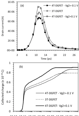
The drain current transients produced by the ion strike are shown in Fig. 3a for a LET value of 1 MeV/(mg/cm2). The drain current peak in 4T-DGFET is higher than in 3T-DGFET for positive Vg2 (and respectively lower for negative Vg2), due to the higher Ioff current (and respectively lower Ioff current for
always higher in DGFET than in 3T-DGFET. In 4T-DGFET, the control by the front of the electrostatic potential in the channel is less effective, which enhances the floating body effects and the collected charge and the parasitic bipolar amplification (Fig. 4) are higher.
1E-11 1E-10 1E-09 1E-08 1E-07 1E-06 1E-05 1E-04 0 0.2 0.4 0.6 0.8 1 D ra in c u rr e n t (A )
Front gate voltage Vg1(V)
3T-DGFET
4T-DGFET - Vg2=0.1 V
4T-DGFET - Vg2=-0.1 V
Fig. 2. Drain current characteristics as function of Vg1 for 4T-DGFET with
different back gate biases. The drain current versus Vg of 3T-DGFET is also
reported for comparison. Vd=0.7 V.
0E+00 2E-06 4E-06 6E-06 8E-06 1E-05 2 6 10 14 18 22 26 D ra in c u rr e n t (A ) Time (ps) 4T-DGFET - Vg2=-0.1 V 3T-DGFET 4T-DGFET - Vg2=0.1 V 0 0.2 0.4 0.6 0.8 1
1E-12 1E-11 1E-10 1E-09 1E-08 1E-07 1E-06 1E-05
C o ll e c te d c h a rg e ( x 1 0 -1 6C ) Time (s) 4T-DGFET - Vg2=-0.1 V 3T-DGFET 4T-DGFET- Vg2=0.1 V
Fig. 3. Drain current transient (a) and collected charge (b) in 3T-DGFET and 4T-DGFET withVg2=0.1 V and Vg2=-0.1 V. The transistors are biased in
off-state (Vg=0 V for 3T-DGFET and Vg1=0 V for 4T-DGFET) and Vd = 0.7 V.
The ion strike LET is 1 MeV/(mg/cm2).
(a)
0 1 2 3 4 5 0.1 1 10 100 B ip o la r a m p li fi c a ti o n LET (MeV/(mg/cm2)) 3T-DGFET 4T-DGFET - Vg2=-0.1 V 4T-DGFET - Vg2=0.1 V
Fig. 4. Bipolar amplification as function of LET in 3T-DGFET and 4T-DGFET at Vg2=0.1 V and Vg2=-0.1 V.
IV. FinFET
Static drain current characteristics as function of front gate bias in 4T-FinFET at different Vg2 and in 3T-FinFET are shown in Fig. 5. In 3T-FinFET the gate better controls the potential in the silicon body and reduces short-channel effects. Then, Ioff in 3T-FinFET is slightly lower than Ioff in 4T-FinFET with Vg2=0 V (Fig. 5) and the subthreshold slope is improved in 3T-FinFET compared to 4T-FinFET.
3D electron density profile in the silicon film of 3T-FinFET and 4T-FinFET at Vg2=-0.1 V, before the ion strike, is presented
in Fig. 6. In 4T-FinFET, near the back gate (gate 2) interface the electron density is lower than that of 3T-FinFET due to the negative bias of the back gate. 2D electron density in a vertical cross section perpendicular to the gates (C-C’ cross-section shown in Fig. 6) confirms this observation.
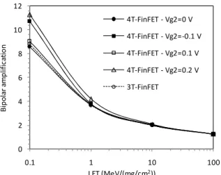
Similar to Planar DGFET configuration, the peak of the drain current transient in 4T-FinFET is higher than in 3T-FinFET for positive Vg2 and smaller for negative Vg2 (Fig. 8). The bipolar amplification (presented in Fig. 8 for an ion strike in vertical incidence) increases (at low LET) with the increase of positive Vg2 and with the decrease of the negative Vg2.
1E-09 1E-08 1E-07 1E-06 1E-05 1E-04 1E-03 0 0.1 0.2 0.3 0.4 0.5 0.6 0.7 D ra in c u rr e n t (A )
Front gate voltage Vg1(V) 3T-FinFET
4T-FinFET - Vg2=-0.1 V
4T-FinFET - Vg2=0 V
4T-FinFET - Vg2=0.1 V
Fig. 5. Drain current characteristics as function of Vg1 for 4T-DGFET at
different back gate biases. The drain current curve versus Vg in 3T-FinFET is
also shown. Vd=0.7 V.
3T-FinFET
4T-FinFET
BOX BOX D S D S Gate 2 Gate 1 A-A’Fig. 6. 3D profile of electron density in the 3T- FinFET and 4T-FinFET at Vg2=-0.1 V before the ion strike. For a better view the gate material, oxide
gate and spacers are not shown. Vg=0 V for 3T-FinFET and Vg1=0 V for
4T-FinFET. Vd=0.7 V.
3T-FinFET 4T-FinFET 3T-FinFET 4T-FinFET
Bef ore ion strike t=10 ps
Fig. 7. 2D profile of electron density in a vertical cross-section (A-A’ plane defined in Fig. 6) in the middle of the channel of 3D FinFET before the ion strike and at t = 10 ps (maximum charge generation). The gate material and a part of the buried oxide are not shown. Vg=0 V for 3T-FinFET. Vg1=0 V and
Vg2=-0.1 V for 4T-FinFET. Vd=0.7 V. The ion strike LET is 1
MeV/(mg/cm2). 0E+00 2E-06 4E-06 6E-06 8E-06 1E-05 1E-05 2 6 10 14 18 22 26 D ra in c u rr e n t (A ) Time (ps) Vg2=0.1 V Vg2=0 V Vg2=-0.1 V Vg2=-0.2 V Vg2=0.2 V 3T-FinFET 4T-FinFET
Fig. 8. Drain current transients in 3T-FinFET and 4T-FinFET (at different back gate biases) for an ion strike in vertical incidence. The transistors are biased in off-state (Vg=0 V for 3T-FinFET and Vg1=0 V for 4T-FinFET) and
0 2 4 6 8 10 0.1 1 10 100 B ip o la r a m p li fi c a ti o n LET (MeV/(mg/cm2)) 4T-FinFET - Vg2=0 V 4T-FinFET - Vg2=-0.1 V 4T-FinFET - Vg2=0.1 V 4T-FinFET - Vg2=0.2 V 3T-FinFET
Fig. 9. Bipolar amplification versus LET in 3T-FinFET and 4T-FinFET (at different back gate biases) for an ion strike in vertical incidence. The transistors are biased in off-state (Vg=0 V for 3T-DGFET and Vg1=0 V for
4T-DGFET) and Vd = 0.7 V.
V. DISCUSSION
To facilitate the comparison between FinFET and Planar DGFET, we simulate the transient response for an ion striking horizontally, parallel to the z-axis (perpendicular to the gates, direction “2”) in 4T-FinFET. Figure 10 compares drain current transients in 4T-FinFET for the two ion strike directions. The simulation results show that the peak of the drain current transient is lower for a horizontal ion strike than for a vertical ion strike. The collected charge is smaller for an ion striking horizontally on the gates of 4T-FinFET than for a vertical strike, because of a lower deposited charge. However, the bipolar amplification is higher at low LET for a horizontal strike than for a vertical strike, as shown in Fig. 11.
Finally, the bipolar gain is found to be higher in 4T-FinFET than in 4T-DGFET for all LET values. This is due to the thicker silicon film considered in FinFET architectures (12 nm compared to 6 nm in DGFET). Then, floating body effects are more important in FinFET (because the front gate control over the body potential is less effective), which leads to more important bipolar amplification.
0E+00 2E-06 4E-06 6E-06 8E-06 2 6 10 14 18 22 26 D ra in c u rr e n t (A ) Time (ps) Vg2=0 V Vg2=-0.1 V Vg2=0 V Vg2=-0.1 V Vertical Ion strike Horizontal Ion strike 4T-FinFET
Fig. 10. Drain current transients in 4T-DGFET for vertical and horizontal ion strikes. The ion strike LET is 0.1 MeV/(mg/cm2).
0 2 4 6 8 10 12 0.1 1 10 100 B ip o la r a m p li fi c a ti o n LET (MeV/(mg/cm2)) Vg2=0 V Vg2=-0.1 V Vgb=0 V Vgb=-0.1 V Vertical Ion strike Horizontal Ion strike
Fig. 11. Bipolar amplification versus LET in 4T-DGFET for vertical and horizontal ion strikes.
VI. CONCLUSION
This paper presents the transient response to heavy ion irradiation of independent gate (4 terminals) DGFET and FinFET. The bipolar gain and charge collection of 4T-DGFET and 4T-FinFET are analyzed as function of LET and ion strike location, and compared to that of 3T-DGET and 3T-FinFET, respectively. Our results show that the bipolar amplification is higher in independent-gates devices for both positive and negative back gate bias. The bipolar gain of FinFET is found to be higher than the bipolar amplification of DGFET, due to the thicker silicon body considered for the first architecture.
REFERENCES
[1] W. Haensch, E. J. Nowak, R. H. Dennard, P. M. Solomon, A. Bryant, O.H. Dokumaci, A. Kumar, X. Wang, J. B. Johnson, M. V. Fischetti, “Silicon CMOS devices beyond scaling”, IBM J. Res Develop., vol. 50, no. 4/5, pp. 339-361, 2006.
[2] M. Masahara, Y. Liu, K. Sakamoto, K. Endo, T. Matsukawa, K. Ishii, T. Sekigawa, H. Yamauchi et al., “Demonstration, Analysis, and Device Design Considerations for Independent DG MOSFETs”, IEEE Trans. Electron. Dev. 52, pp. 2046-2051, 2005.
[3] G. Pei and E.C. Kan, “Independently Driven DG MOSFETs for Mixed-Signal Circuits: Part I—Quasi-Static and Nonquasi-Static Channel Coupling”, IEEE Trans. Electron. Dev. 51, 2086-2093, 2004. [4] L. Mathew, Y. Du, A.V. Thean, M. Sadd, A. Vandooren, C. Parker, et
al., “CMOS vertical Multiple Independent Gate Field Effect Transistor (MIGFET)”, in Proc. IEEE Int. SOI Conf., Oct. 2004, pp. 187–189. [5] K. Castellani, D. Munteanu, J.L. Autran, V. Ferlet-Cavrois, P. Paillet, J.
Baggio, “Simulation Analysis of the Bipolar Amplification Induced by Heavy-Ion Irradiation in Double-Gate MOSFETs”, IEEE Trans. Nucl.
Sci., vol. 52, no. 6, pp. 2137-2143, Dec. 2005.
[6] D. Munteanu, V. Ferlet-Cavrois, J.L. Autran, P. Paillet, J. Baggio, O. Faynot, C. Jahan, L. Tosti, “Investigation of Quantum Effects in Ultra-Thin Body Single- and Double-Gate Devices Submitted to Heavy Ion Irradiation”, IEEE Trans. Nucl. Sci., vol. 53, no. 6, pp. 3363, 2006. [7] D. Munteanu, J. L. Autran, V. Ferlet-Cavrois, P. Paillet, J. Baggio, K.
Castellani, “3-D Quantum Numerical Simulation of Single-Event Transients in Multiple-Gate Nanowire MOSFETs”, IEEE Trans. Nucl.
Sci., vol. 54, no. 4, pp. 994-1001, Aug. 2007.
[8] M. Vinet, T. Poiroux, J. Widiez, J. Lolivier, B. Previtali, C. Vizioz, et al., “Bonded Planar Double-Metal-Gate NMOS Transistors Down to 10 nm”, IEEE Electron Dev. Lett., vol. 26, no. 5, pp. 317-319, May 2005. [9] Z. Lu and J. G. Fossum, “Short-channel effects in Independent-Gate
FinFETs” IEEE Electron Dev. Lett., vol. 28, no. 2, pp. 145, Feb. 2007. [10] Synopsys Sentaurus TCAD tools, Available online: