HAL Id: tel-03131528
https://tel.archives-ouvertes.fr/tel-03131528
Submitted on 4 Feb 2021HAL is a multi-disciplinary open access archive for the deposit and dissemination of sci-entific research documents, whether they are pub-lished or not. The documents may come from teaching and research institutions in France or
L’archive ouverte pluridisciplinaire HAL, est destinée au dépôt et à la diffusion de documents scientifiques de niveau recherche, publiés ou non, émanant des établissements d’enseignement et de recherche français ou étrangers, des laboratoires
Integrated Circuit Authentication based on
electromagnetic signature
Mosabbah Mushir Ahmed
To cite this version:
Mosabbah Mushir Ahmed. Integrated Circuit Authentication based on electromagnetic signature. Optics / Photonic. Université Grenoble Alpes, 2019. English. �NNT : 2019GREAT005�. �tel-03131528�
DOCTEUR DE LA
COMMUNAUTÉ UNIVERSITÉ GRENOBLE ALPES
Spécialité : OPTIQUE ET RADIOFREQUENCESArrêté ministériel : 25 mai 2016
Présentée par
Mosabbah Mushir AHMED
Thèse dirigée par Etienne PERRETet codirigée par David HELY, Maitre de Conférence, Communauté Université Grenoble Alpes
et Maxime BERNIER, Maître de Conférences, Université Savoie Mont Blanc (USMB)
préparée au sein du Laboratoire Laboratoire de conception et d'intégration des systèmes
dans l'École Doctorale Electronique, Electrotechnique, Automatique, Traitement du Signal (EEATS)
Authentification de puces électroniques par
des approches RF et THz non intrusives
Integrated Circuit Authentication based on
electromagnetic signature.
Thèse soutenue publiquement le 4 février 2019, devant le jury composé de :
Monsieur ETIENNE PERRET
MAITRE DE CONFERENCES, GRENOBLE INP, Directeur de thèse Monsieur NUNO BORGES CARVALHO
PROFESSEUR, UNIVERSITE D'AVEIRO - PORTUGAL, Rapporteur Monsieur BRUNO ROUZEYRE
PROFESSEUR, UNIVERSITE DE MONTPELLIER, Rapporteur Monsieur DAVID HELY
PROFESSEUR ASSOCIE, GRENOBLE INP, Co-directeur de thèse Monsieur WENCESLAS RAHAJANDRAIBE
PROFESSEUR, UNIVERSITE AIX-MARSEILLE, Président Monsieur MAXIME BERNIER
PROFESSEUR ASSOCIE, UNIVERSITE SAVOIE-MONT-BLANC, Examinateur
Acknowledgement
Firstly, I would like to express my sincere gratitude to my thesis director Prof. Etienne Perret for providing me the opportunity to do my thesis in LCIS - INP Grenoble. I would like to gratefully thank Prof. Etienne Perret and my co-supervisor Prof. David Hely, of LCIS – INP Grenoble, Valence, for the continuous support of my PhD study and related research, for their patience, motivation, and immense knowledge. Their guidance helped me in all the time of research and writing of this thesis. I could not have imagined having a better advisors and mentors for my PhD study.
I would also like to thank the rest of my thesis committee: Prof. Romain Siragusa and Prof. Nicolas Barbot of LCIS - INP Grenoble, Valence and Prof. Frederic Garet and Prof. Maxime Bernier, University of Savoie Mount Blanc, Chambery, for their insightful comments and encouragement, but also for the hard question which incented me to widen my research from various perspectives.
My special thanks to my office mates Zeshan and Kostas, for extending their amicable relation, support and for all the fun we have had in the last three years. I would like to thank my fellow lab-mates, Marco, Bony, Hatem, Thanos for their valuable support. I would like to extend special thanks to the administrative team of LCIS – Jennyfer Duberville, Carole Seyvet, Romain Doleux and Caroline Palisse for helping with all sorts of pile of administrative papers. My special thanks to M. Cedric Carlotti (IT administrator) for keeping my laptop and system running smoothly throughout my PhD period. Also I thank my friend Kashif Nawaz from UC Louvain, Belgium for discussing all the ideas related to the field of hardware security.
Last but not the least; I would like to thank my wife, for her patience and undue support with me, my parents and to my brothers for supporting me spiritually throughout writing this thesis and my life in general.
Abstract
The advent of nano-scale device or shrinking of integrated circuits (IC) has become a blessing for the human civilization. Nowadays it has become very much common to find piece of electronic devices in different applications and instruments of various sectors. ICs now are not only confined to computers and mobiles but they are integral part of our everyday life. They can be found in our kitchens (in microwaves, oven), in hospitals (instruments such as ECG, MRI etc.), banks, space, telecom, defense etc. It has of course made our lives easier. However everything comes with a price.
The change in economy due to the integration of electronics in different domains has put an extra pressure on companies and manufacturers to produce their product in tighter constraints in terms of cost and time. This has led to companies off shoring their manufacturing units to foundries beyond their direct control. Due to this advent of small and untrusted foundries have been on rise. The rise in various manufacturing units or foundries has given rise to the phenomenon of counterfeiting of electronic components especially ICs. For smaller foundries who do not meet all the specification, if they get hand to the design of the circuit layout, they can produce the IC similar to the one developed by original component manufacturers (OCMs) and sell them into market without consent of OCM and without performing standardized tests. Also, the malicious or untrusted foundries can copy and clone the netlist of devices and sell under the name of OCM. Various types of counterfeit ICs – recycled, remarked overproduced, out-of-spec/defective, cloned, forged documentation, and tampered – have made the supply chain vulnerable to various attacks. However, due to the lack of efficient detection and avoidance techniques, many more instances of counterfeit ICs evade detection than those that are actually detected. Over last few years the rise in the incidents of IC counterfeit has propelled the designer and researchers to develop various testing and standardization methods in place. However, many of these methods can be cumbersome and have huge implications and costs for their implementations. This can be discouraging for the users and OCMs to implement these methods in their product.
In this dissertation, we have worked on the implementation of methodology that can be used to generate fingerprints or signatures form the ICs which can be used for the purpose of their authentication. The method adopted in this work is based on the idea of exploiting the manufacturing induced process variations by implementing the electromagnetic (EM) waves. The manufacturing variability of various devices under test has been exploited through use of EM waves. The use of EM waves has been studied in detail along with the various implications of using and generating them in the IC. This dissertation uses two methodologies to utilize EM wave for the exploitation of the process variation effects. The exploited process variation effects have been subjected to mathematical treatments to quantify the response statistically.
The following tasks have been implemented in this work:
State of the art study of IC counterfeiting and IC cloning (on both risk and mitigation techniques). Measurement set-up: Component choices, board measurement development.
Circuit configuration to maximize the measurement sensitivity. Measurement campaigns using different approaches (RF based).
Measurement Exploitation in order to extract authentication information from the measurement. Together with the implementation of EM based approaches on new device, we have also worked on observing the effects of the aging on the devices under test and particularly on the authentication metrics themselves. For this we have setup measurement test benches and put the device under accelerated stress to induce the aging effects.
To validate our work, we have performed our measurements across various devices of same manufacturer and family. This work has focused on using two different semiconductor devices i.e. FPGA and microcontrollers. These are highly used devices and find their application in various domains. The statistical computation after mathematical treatment of responses, gives the error rate which determines the efficiency of the methodologies adopted.
Contents:
1. Introduction... 13
1.1 Motivation ... 14
1.2 Contributions of this work... 16
1.3 Organization of thesis ... 21
2. Counterfeiting of IC: detection, avoidance and preview on EM based authentication techniques ... 24
2.1 Counterfeit IC: definition and features... 25
2.2 Counterfeit Detection ... 29
2.3 Counterfeit avoidance techniques ... 33
2.4. PUF based approach – authentication principle and advantages ... 35
2.5 Preview on EM based techniques for authentication ... 38
2.6 Conclusion ... 42
3. Radiated Electromagnetic technique (REMT) for IC authentication ... 46
3.1 Preliminaries and objectives... 46
3.2 Process Variations in IC ... 47
3.3. Electromagnetic (EM) emission in IC ... 49
3.4. Radiated EM emission for authentication of FPGA-IC ... 50
3.5. EM emission from FPGA – Measurements and Results... 59
3.6. MCU authentication – EM emission technique ... 70
3.7 FPGA and MCU: final discussion ... 79
4. Effects of aging on authentication of FPGA using REMT based approach... 83
4.1. CMOS Transistor Aging Mechanisms ... 83
4.2 Effects of NBTI and HCI on the digital circuit... 86
4.4 Effects of aging on multiple ROs technique ... 96
4.5. Post-processing techniques (Encoding metrics) ... 97
4.6. Inferences from the aging effects on multiple RO ... 103
4.7. Conclusion from REMT – along with aging effects... 104
5. Guide Electromagnetic based Authentication Techniques for IC ... 107
5.1 GEMT based authentication method – an overview of principle ... 110
5.2. GEMT based authentication – objective ... 114
5.3 Simulation model of IC in CST... 115
5.4. Hardware Design and Measurement for GEMT method ... 119
5.5 Results from GEMT measurements... 124
5.6 Binary fingerprint generation ... 130
5.7 Multi-route implementations in GEMT based method ... 136
5.8. Limitations and drawbacks of GEMT based technique... 141
5.9. Conclusion and discussion of GEMT based approach ... 142
5.10 Overall summary of authentication mechanism... 144
6. Application of RF-FPGA PCB: Reconfigurable RF platform and RF wireless communication... 148
6.1 Motivation: FPGA based RF devices ... 149
6.2. Motivation: FPGA based RF wireless communication ... 150
6.3. FPGA as RF devices ... 151
6.4 RF wireless communication between FPGA boards... 164
6.5 Conclusion ... 182
List of Figures :
Fig.1.1: A high level illustration of EM based technique for authentication highlighting different steps used. (a) For new IC when it is not used for any application. (b) For an aged or used IC. ...19 Fig. 2.1: Taxonomy of various techniques of counterfeit ICs...26 Fig. 2.2: Different stages of IC manufacturing and counterfeiting techniques at various stages of manufacturing. ..28 Fig. 2.3: (a) A pictorial description of CMOS Arbiter PUF with MUX and Latch. (b) Typical phases of PUF working to
combat counterfeiting. ...36 Fig 2.4: Post-processing steps implemented for converting the IC response into fingerprints / signatures. ...39 Fig 3.2: EM field in an IC and depiction of coupling mechanisms of electric and magnetic fields in an IC. ...50 Fig.3.3: A use case showing various steps required to implement radiated EM based authentication schemes. The
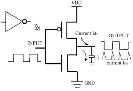
vendor or OCM generates and stores fingerprints. A user can use same authentication protocol (EM based) to authenticate the DUT. ...53 Fig 3.4: Three-stage RO. (a) Circuit diagram of three-stage RO. (b) Timing diagram of three-stage RO. ...55 Fig 3.5: CMOS inverter with input-output waveform and output current (Ids). ...56 Fig 3.6: Frequency of RO for varying interconnect lengths and no. of stages of inverter (showi ng fundamental
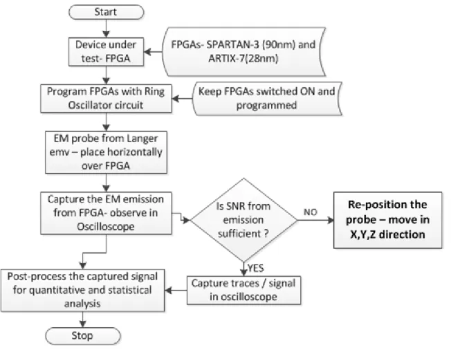
frequency as well as the higher harmonics). (a) A 3-stage inverters RO (b) A 5-stage inverter RO (c) A 3-stage inverters RO with longer interconnect length between logic elements. ...57 Fig. 3.7: A complete flowchart describing the measurement steps performed for capturing the EM emission from
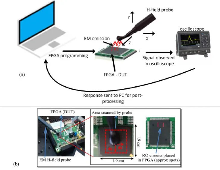
the FPGA DUTs...61 Fig 3.8: Measurement setup: FPGA board with probe (a) REMT measurement steps employed in the study with
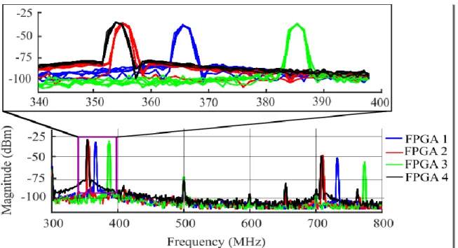
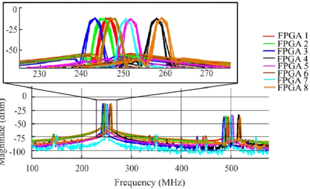
different instruments. (b) Inset: area scanned by H-field probe in XY-direction, where dx = dy = 1 mm is the unit distance and approximate spot, where RO circuit is placed in the FPGA. ...63 Fig 3.9: RF signals emitted by four different ARTIX-7 FPGAs with the same RO circuit in bandwidth up to 800 MHz
and (inset) a zoomed-in view around the fundamental frequency peak (exhibiting the repetitive
measurements). ...64 Fig 3.10: Cosine Similarity score distribution of inter and intra variability for all measurements of: (a) ARTIX -7, and
(b) SPARTAN-3E FP GA. ...66 Fig. 3.11: Error probability curves depicting FAR and FRR for: (a) ARTIX- 7. (b) SP ARTAN -3E. ...66 Fig 3.12: EM signals emitted by four different SPARTAN-3E FPGAs with the same RO circuit in bandwidth up to 500
MHz and (inset) a zoomed-in view around the fundamental frequency peak (exhibiting the repetitive
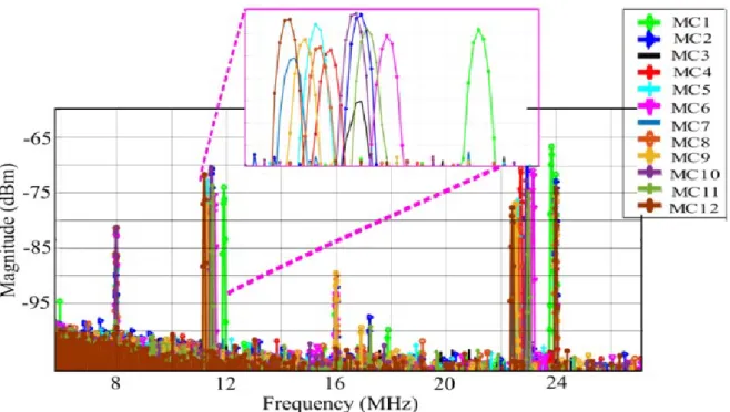
measurements). ...68 Fig. 3.13: Measurement steps for STM32 µC: Localized EM probe horizontally placed over the IC of μC board. ...72 Fig. 3.14: EM emission due to clock from the different MCUs. The EM emission is captured using H-field probe and observed in oscilloscope / spectrum analyzer. ...72 Fig. 3.15: Description of the RESET circuit of STM32F103RB. ...73 Fig. 3.17: EM emitted by 12 different MCUs due to external reset depicted in the bandwidth up to 25 MHz and
(inset) a zoomed-in view around the fundamental frequency peak. ...76 Fig: 3.18: Statistical distribution of the inter and intra variability. (a) Histogram showing distribution of inter and
intra variability. (b) Error probability curve to observe the overlap of the FAR and FRR curve. ...78 Fig.4.1: HCI based aging mechanism in a NMOS CMOS based transistor. ...85 Fig. 4.2: Various stages of inverter outputs showing the effects of HCI and NBTI. (a) A basic CMOS inverter circuit
Fig. 4.3: Effects on the Vth voltage due to the aging phenomenon such as HCI and NBTI. The effect is modeled with power law time dependence. ...88 Fig. 4.4: A use case scenario we have defined explaining the effects of aging on the authentication methodologies.
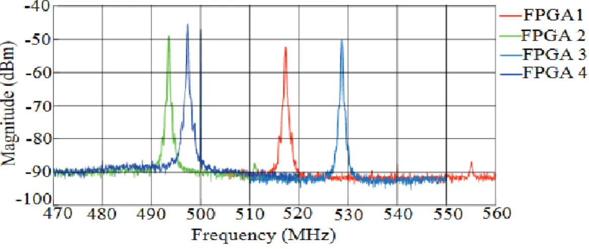
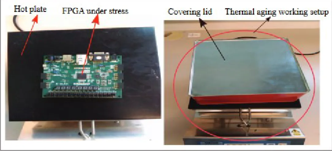
(a) One RO technique is depicted and its subsequent responses with and without aging effects. (b) Multiple ROs technique is depicted along with the responses with and without aging effects. ...89 Fig 4.5: RO frequency obtained using radiated EM emission of four ARTIX -7 FPGAs when fresh (no aging effects)..91 Fig. 4.6: Experimental setup adopted to age the FGPA through accelerated thermal stress...92 Fig. 4.7: Shift in RO frequency with aging. The insert zoom shows a zoom on the RO frequency after accelerated
aging. ...93 Fig. 4.8: RO frequency degradation curve of frequency with time. ...93 Fig. 4.9: A pictorial depiction highlighting the placement floor plan of FPGA that is used to place 16 ROs manually
across the FPGA...95 Fig. 4.10: Pattern (response) of 16 RO frequencies for four FPGAs. Each FPGA has distinct pattern due to 16 ROs
(intra-die variability). ...96 Fig. 4.11: Shift or change in the pattern of RO frequencies after FPGA (ROs I FPGA) have been subjected to
accelerated aging through thermal s tress for two weeks of time. ...97 Fig. 4.12: Mean based encoding scheme illustrated with a pictorial depiction. ...99 Fig. 4.13: A graphical illustration of frequency pair comparison metric... 101 Fig. 5.1. An illustration of using IC on a pluggable socket to be characterized with the guided RF waves. In this type
of measurement a dedicated PCB is used that incorporates al l RF features (RF ports etc.) for the purpose of measurement... 108 Fig. 5.2: A pictorial depiction of using ICs from same wafer (manufacturer, series) to perform a guided RF wave
measurement for the purpose of generating their signature or fingerprint. ... 109_Toc530485416
Fig. 5.3: Use case showing a methodology for guided RF usage for IC authentication. ... 111 Fig. 5.4: Proposed hardware model of EM based authentication with a testbench. This testbench is specifically
made to use RF signal as excitation to the IC... 112 Fig. 5.5: Physical model and structure of IC. (a) CST model of a 56 pin IC. (b) A physical model of IC. ... 115 Fig. 5.6: CST chip model description: (a) CST Chip Model of package with dimensions. (b) Discrete port used for S
parameter... 116 Fig. 5.7: S21 response without any interconnect, amount of power transmitted is very low around -30dB. ... 117 Fig. 5.8: Shift in the length of interconnects in the IC model in CST simulation. The difference between Length1 and Length2 is around 0.05mm. ... 117 Fig. 5.9: S21 (transmission coefficient) difference due to change in route inside IC, observe the shift in the
frequency of S21 due to routing lengths differences. ... 118 Fig. 5.10: Surface current on the route established between input-output port in CST simulation of an IC at two
frequencies (a) at 6 GHz and (b) 9 GHz. ... 118 Fig. 5.11: PCB Board for the measurement for SPARTAN 3A FPGA. The detailed illustration shows the various circuit
components used along with the SPARTAN-3A FPGA. For RF IO connection SMA connectors are used. ... 120 Fig. 5.12: Measurement setup on the customized FPGA PCB to perform the RF test. Inset zoom shows an enlarge
description of 50 Ohms resistors used with the transmission for proper matching. Input-Output (IO) ports naming is described which is used throughout this study... 121 Fig. 5.13: Equivalent models. (a) An equivalent circuit model for a wire. (b) An equivalent capacitive load for the
buffer circuit... 123 Fig. 5.14: Two different routes implemented for same buffer “B” on same input-output ports (A and D). (a) Shorter interconnect(route) between IO ‘A’ and ‘D’. (b) Longer interconnect(route) between IO ‘A’ and ‘D’. ... 124 Fig. 5.15: S21 response from the 11 FPGA for two different routes with each measurement done 10 times. Inset
CS score distribution of inter and intra variability for route 1. (d) CS score distribution of inter and intra variability for route 2... 127 Fig.5.18: A use case showing the conca tenation of two routes response for one FPGA. ... 128 Fig.5.19: Results after concatenating the routes. (a) The error probability curves showing the distinction and
overlap between FAR and FRR when the processing is done with the combined or concatenated routes for all the FPGAs. Inset zoom of overlap of FAR and FRR. (b) Change (decreasing trend) in error probability between separate and concatenated routes... 129 In order to utilize the S21 curve into generating the binary fingerprints, the steps adopted is shown in Fig. 5.20.
Applying the procedure from Fig. 5.20, we can utilize the frequency and forward transmission coefficient (FTC) relationship. This relationship determines the selection of few points over the curve which can give frequency values, which are further encoded into binary fingerprints. In order to generate the binary fingerprints from the response, the results from the two curves have been concatenated or combined together. A detailed procedure is given below in next sub-section. ... 130 Fig. 5.20: Generating binary coded fingerprints using binary encoding technique code from S21 curves response
from two routes. The relation between power and frequency is used as a metric... 131 Fig. 5.21: An illustration to highlight the steps used in using the FTC response i n order to convert the frequency
values into binary fingerprints. Inset zoom on the small range of S21 magnitude used. ... 132 Fig. 5.22: Hamming Distance and error probability curves. (a) Hamming distance between inter and intra devices.
(b) Error probability curves between FAR and FRR. Inset zoom on overlap of FAR and FRR. ... 134 Fig. 5.23. Multi-route technique adopted in order to mitigate error and aging effects. (a) Depiction showing the
two or multiple routes on same IO ports. (b) Both the routes have been separately shown for clarity. ... 137 Fig. 5.24: S21 response from the two routes and the differences between the responses from two rou tes on two
FPGAs. ... 137 Fig. 5.25: Difference in the magnitude of S21 response to mitigate the effects for systematic and aging rela ted
error. (a) S21 response from the two routes. (b) Difference in magnitude of the S21 response for various FPGAs. (c) The error probability curves showing the distinction and overlap between FAR and FRR when the processing is done with the difference of the routes for all the FPGAs. Inset zoom of overlap of FAR and FRR. ... 139 Fig. 5.26: Implementation of XOR gate to find the difference between two routes – based on phase difference
between RF waves on two routes... 140 Fig. 5.27: The response from the XOR based implementation on 5 FPGAs. The peak frequencies have also been
shown in legend. ... 140 The response from Fig. 5.27 shows a di stinction which points for the fact that FPGAs can be distinguished using this
technique also. The authentication part of the study using the XOR based technique can be one of the interesting aspects for the future work. ... 141 Fig. 6.1: (a) Measurement setup on the customized FPGA PCB to perform the RF test. Inset zoom shows an enlarge
description of 50 Ohms resistors used with the transmission for proper matching. Input-Output (IO) ports naming is described which is used throughout this letter. (b) Proposed methodology to make a FPGA work as RF device by generating different bit streams e.g. Switches depending on the input output ch osen... 153 To highlight the validity of this scheme, we have implemented few basic RF devices using FPGAs. In the sections
below we have given an elaborated description of each RF devices implemented in FPGA. ... 153 Fig. 6.2: Transmission characteristics and input-output power relationship. (a) Transmission characteristics (S21)
for different power levels. The input RF signal is sent through port ‘C’ and output through port ‘Y’ as described in Fig. 6.1(b). (b) Relationship between input and output power at frequenc y 100 MHz and 500 MHz... 155
Fig. 6.3: Characteristics of S-parameter with and without matching and S21 characteristics for lower i nput power range. (a) S11 parameter response measured without DC bias - direct transmission lines with 50 Ohms resistors and with RLC network. Also shown is S12 parameter (without DC bias on port 2). (b) S21
characteristics for very low input power level up to frequency of 1 GHz... 156 Fig. 6.4: A time domain measurement setup. The instruments used are: RF signal generator to inset RF signal. DC
bias tee for the voltage biasing. Oscilloscope is used to observe the output. ... 157 Fig. 6.5: Time and Frequency domain (FFT of time domain) response at : (a) 700 MHz (b) 200 MHz at its higher
harmonics at around 400 MHz. ... 158 Fig. 6.6: Classical RF switches schematics. (a) Single pole single throw (SPST) switch. (b) Single pole double throw
(SPDT) switch. ... 159 Fig. 6.7: FPGA programmed with AND gate to realize a RF SPST switch. Port ‘A’ is used as input and port X as
output. Ports ‘A’ and ‘X’ are connected to port 1 and 2 of the vector network analyzer (VNA), respectively. In FPGA internally, an AND gate is implemented as look up table. For simplicity an equivalent AND gate
schematic is shown here... 160 Fig. 6.8: Response from FPGA with a buffer configured between port A(input) & port X (output) for input power of
10 dBm : Transmission (S21),reverse transmission (S12) ,reflection (S11) and isolation (switch OFF) curves.160 Fig. 6.9: (a) Switch configuration analogous to a SPDT switch implemented in FPGA. Port B as input and E as output
and its S-parameter response, similarly in (b) Port B as input and port C as output and it S-parameter response. In FPGA internally, an AND gate is implemented as look up table. For simplicity an equivalent AND gate schematic is shown here... 162 Fig. 6.10: Power splitter and its responses. (a) FPGA configured as a power splitter using two buffers circuit. (b) S
-parameter responses of the power splitter. (c) Phase difference between two routes. ... 163 Fig. 6.11: Description of PCB for communication system, the programming scheme of the FPGA to generate
bitstream, and an end-to-end wireless communication between two FPGAs. ... 164 Fig. 6.12: OOK transmitter and receiver block classically implemented. (b) Modulator / Transmitter block. (b)
Receiver / demodulator block. ... 166 Fig. 6.13: OOK modulator circuit implemented in FPGA using RO and MUX circuit. RO circuit is used in order to
generate a CW signal of high frequency. MUX is used as a switch where baseband signal of low frequency is externally fed which controls the state of MUX output. ... 167 Fig. 6.14: Description of CW and baseband signals in time and frequency domain. (a) CW signal and baseband
signal in frequency domain. (b) CW and baseband signal in time domain representation. Inset an enlarged representation of the modulated signal. ... 169 Fig. 6.15: Buffers used for the OOK demodulation. (a) Series of buffers that can be depicted as envelope detector
for demodulation of OOK signal. (b) Simulation results of implementing series of buffers as OOK demodulator in LTSpice®. (c) Frequency domain response by varying the number of buffers in series... 171 Fig 6.16. Measurement results - buffers as demodulator with PWM modulated input. The response is observed
using oscilloscope. ... 172 Fig. 6.17: Description of the customized dipole antenna used. (a) Structure of the half wave dipole antenna. (b)
Frequency response (S11) and phase response of the antenna. ... 173 Fig. 6.18: Measurement setups. (a) Measurement setup used in transmission of wireless data between two FPGAs
using customized dipole antenna. After the antenna on the Rx side, we have the option to use PA. (b) Actual measurement setup used in experimentation in real environment. (Inset) the half wave dipole antenna developed in-house for bandwidth of around 240 MHz... 174 Fig. 6.19: Waveforms showing the input baseband signal and the output demodulated signal at the receiver (Rx)
FPGA. (a) Time domain response of the transmitted and received (demodulated signal) observed in oscilloscope. (b) Frequency domain response of the transmitted and received signal observed in spectrum analyzer... 175
Fig. 6.21: An example of distributed task over two FPGAs. (a) A half adder implementation implemented on two FPGAs. Signal ‘A’ on transmitter FPGA is added with signal ‘B’ on the receiver FPGA. (b) Waveform of the input ‘A’ and ‘B’ and their sum and carry is shown. ... 178 Fig. 6.22: Description of increasing CW frequency by using XOR gate. (a) General description of XOR gate and its
input-output wavefor m. (b) Scheme incorporated to enhance the CW frequency of modulator on FPGA. ... 180 Fig. 6.23: Results waveforms for the XOR operation to increase CW frequency. (a) Time domain representation of
the RO, RO+ π/2 and after XOR gate waveforms. (b) Frequency domain representations of original RO (CW frequency) and CW frequency after using XOR gate. ... 181
List of Tables:
Table 2.1: Top-5 Most Counterfeited Semiconductors in year 2011. ...25
Table2.2: Description of physical inspection methods ...31
Table 2.3: Different methods of counterfei t detection for various counterfeit techniques ...33
Table 2.4 : Different methods used for the IC counterfeit avoidance...35
Table 3.1 : Description of the EM probe...60
Table 3.3 : Frequency of ARTIX-7 and SPARTAN-3 FPGAs measured in MHz for different numbers of boards in test. ...65
Table 3.4 : Mean and 3 sigma of inter and intra variability. ...77
Table 4.1: Binary vector for each FPGA using Mean deviation methodology ...99
Table 4.2 : Binary vector for each FPGA using frequency pair difference ... 101
Table 4.3: Binary vectors using both metrics after accelerated aging of FPGA3 (FPGA under stress) ... 102
Table 5.1: Example of the differ ence between gray and binary code for two consecutive values ... 133
List of publications:
Mosabbah Mushir Ahmed, D.Hely, R.Siragusa, E.Perret,N.Barbott,F.Garet, M.Bernier
“Authentication of Microcontroller board using non-invasive EM emission technique” in 3rd
International Verification and Security Workshop 2018 (IVSW’18), Costa Brava, Spain. DOI: 10.1109/IVSW.2018.8494883
Mosabbah Mushir Ahmed, D.Hely, R.Siragusa, E.Perret,N.Barbott,F.Garet, M.Bernier “Towards a
robust and efficient EM based authentication of FPGA against counterfeiting and recycling” in
19th CSI International Symposium on Computer Architecture & Digital Systems, Dec. 2017, IEEE CADS. DOI: 10.1109/CADS.2017.8310673
Mosabbah Mushir Ahmed, D.Hely, R.Siragusa, E.Perret,N.Barbott,F.Garet, M.Bernier “Radiated
Electromagnetic Emission for Integrated Circuit Authentication” in IEEE Microwave and
Wireless Components Letters PP(99): 1028 - 1030, Sept 2017, DOI: 10.1109/LMWC.2017.2750078.
Mosabbah Mushir Ahmed, D.Hely, R.Siragusa, E.Perret,N.Barbott,F.Garet, M.Bernier
“Authentication of IC based on Electromagnetic Signature” TRUDEVICE - 6th Conference on Trustworthy Manufacturing and Utilization of Secure Devices (TRUDEVICE 2016), Barcelona, 14-16 November, 2014-16. URL: http://hdl.handle.net/2117/99321
Chapter 1 Introduction
1. Introduction
IC or Integrated circuits find their usage in multiple applications across different domains and sectors. They are used in daily home appliances, smartphones, laptops to more sophisticated systems like banking, military and space exploration etc. Given their usability across very domains, it is imperative to safeguard their integrity against any kind of eternal or internal threats. Hence in a nutshell it can be said that IC are root for a trusted hardware system.
However, in recent times, there have been many incidents related to counterfeit of ICs. A counterfeited IC can pose permanent or temporary damage to the life of a system as well as compromises the integrity of information of the system[1][2]. An IC failure due to a counterfeit part is very serious. When the counterfeit IC fails, it can inflict serious injury, or at a minimum interrupt or delay a mission. It ranks with counterfeit drugs that can cause an individual to be over- or under medicated. Owing to the fact that ICs are used in our day-to-day life - both directly and indirectly - counterfeit ICs also pose major threats to the health, safety, and security of the population at large. For example, the failure of a pacemaker due to a counterfeit component can potentially take someone’s life. A pilot can lose control of his airplane if the IC or electronic components used in that is fake or counterfeited. Hence it not only causes the reliability issues or failure of the system but also inflicts or has the potential to damage the human lives [1].
In addition to the impact on public safety and security, counterfeit ICs could also cause significant damage to the economy. A semiconductor company spends a huge amount of money in developing and marketing a new product, whereas a counterfeiter requires minimal effort to destroy the authenticity of the product. Hence when a fake component with marking of original component manufacturers (OCMs) fails, it tarnishes the reputation and credibility of the OCM. According to studies conducted in [2], around $100 bn. of revenue is lost by legitimate electronics and semiconductor industry due to the incidents of counterfeit. Indeed Hi-Tech industries are significantly affected by this problem. Based on a 2008 report by the International Chamber of Commerce, it was estimated that the cost of counterfeiting and piracy for G20 nations was as much as US$775 billion every year and will grow to $1.7 trillion in 2015 [2][3].
Over the past several years a specialized service of testing has been created for detecting and avoiding counterfeit components. The components must be authenticated by these tests before being placed in
be very time consuming and also involves the risk of damaging the IC or components under test, permanently or temporarily [3][4] . Second method is based on traceability approach to find identity of devices or ICs by using process variation or PV. As discussed, using PV approach, physical unclonable function (PUF) is dominantly used. It exploits the inherent variability of an IC, caused due to manufacturing variations of IC itself. Each PUF contains pair of challenge and response. For each challenge sent to an IC there is a unique response to that challenge [5][6]. Apart from the IC authentication, PUFs are also used for the purpose of secret key generation for cryptographic applications. Bottleneck of the PUF approach is that it requires dedicated on-chip circuitry which may be complex to process and implement. PUFs also have large database of challenge pair response. Apart from the usage of classical techniques and PUF based solutions, research and studies have been going on to develop new approaches that would be effective against counterfeit problems.
With the miniaturization of IC, there are various constraints that arise for the designing any new circuit element in the IC. Area overhead and ease of implementation is major issues that are topic of concerns on IC made on smaller technological nodes. Hence, in terms of adding any extra dedicated circuitry in the IC for the purpose of authentication can be discouraging in terms of economic viability for any OCM. Therefore, it is very important to find for a solution which takes into account the area constraints of IC while implementing solutions to address the issue of counterfeiting. Second important aspect is that the implemented solution should be safe and must not damage the IC in long or short terms.
1.1 Motivation
The motivating factor to perform this study is to introduce and elaborate techniques that can efficiently create a signature of an IC without using any invasive techniques. This will aid greatly in mitigating the problem of area utilization in miniaturized IC. Also, this is a simple scheme that can be effectively used in resource constraint devices. The work in this dissertation is mainly motivated by the following concerns:
1. Counterfeit avoidance and detection requires the utilization of various physical and electrical design factors of the IC. Hence as also stated above in brief, these factors often lead to higher power consumption or higher area occupancy. In particular higher area occupancy utilizes higher Silicon area which in turn increases the cost of the IC. For example, if the instance of physical unclonable functions (PUFs) is taken into account, it is clear from their design approach that this
Chapter 1 Introduction
technique utilizes a considerable amount of IC area. PUFs require a dedicated post-processing unit which is area as well power hogging [5]. This can be demotivating for an OCM to include any extra circuit in its IC for purpose of authentication because of tight budget and time to market constraints Secondly, this can also cost-ineffective for the consumer, who can then be falsely allured in buying the recycled or remarked IC .
2. Subsequently, it is also observed from the above discussion in section 1, that classical techniques like physical inspection use high powered input sources like X-rays, which can damage the IC under test permanent or temporarily [3]. Secondly, these techniques are slow and time consuming for the end user to deploy. Hence, it can be daunting task for the user to employ such a technique which can damage his component and also consume huge amount of time. The technique in this category of electrical inspection is also very time consuming and highly inefficient in terms of detecting the counterfeit [4].
3. One of the major challenges in counterfeit industry is of the recycled IC. Among various IC counterfeit techniques, recycled IC takes around 80% of whole share. Recycled ICs are old ICs sold as new [7]. Hence it is becoming important to understand the difference aspects of old ICs, their characteristics and difference with the new ones. The various techniques adopted have been towards finding and implementing aging based sensors, but they come up with solution to detect old IC. An IC can become aged or old while being in the field. So any authentication process done after the IC has been in the field can discard that IC by putting it in category of recycled IC and in this way even an authentic IC can be discarded.
4. Extending point 3, with the passage of time, the signatures or fingerprints of IC can vary owing to aging and reliability effects on transistors. An IC is always affected by process, temperature and voltage variation when it is employed in the application. Therefore, there is an issue regarding the reliability and aging effects on the principle functions of IC and how it degrades over its usage over the time. An old IC does not mean a fake IC i.e. if a vendor performs an authentication after a time gap of ‘t’ (period in which IC has been used by genuine vendor), it can show deviation in the fingerprints. Hence, it is imperative to have a solution that is gives a fingerprint of IC resistant to aging effects. This is an important aspect that this covered in this dissertation.
using non-invasive approaches. The approaches should be efficient in terms of area and implementation, it should not pose any risk to damage the IC and it should be time efficient and cost effective. Subsequently, it is also an important aspect to extend the implemented technique to cater the aging related problems of the IC. This is to prevent the authentic IC from being discarded due to variation in their fingerprint over time. Hence, in a summary this dissertation answers to the following existing problems in the field of IC authentication:
I. Area overhead of IC utilized in present authentication techniques. II. High cost requirement with the utilization of present techniques.
III. Implementation of authentication techniques in resource constraint devices.
IV. Effects of aging on the obtained fingerprints of IC – authentication valid for lifetime of IC. To answer these concerns, in the next subsection we have highlighted the contribution done in this thesis work.
1.2 Contributions of this work
In view of the problems discussed regarding the counterfeit ICs, and effects they have on system’s reliability and economy; we have made an effort to implement a methodology that is efficient and easy to deploy and handle. It is also discussed in brief in the previous section that there are many studies and research and going to tackle the problem of counterfeiting. This dissertation highlights alternate methods that can be used in order to mitigate counterfeiting of ICs and create fingerprints or signatures of each IC by exploiting their manufacturing process variation or PV.
This dissertation is broadly compiled in the following order.
I. Understanding the effects, features and techniques of counterfeiting of IC. II. Understanding and analysis manufacturing based process variations.
III. Implement EM based techniques to utilize the PV effects to generate unique response from each IC. Perform the measurement steps suitable and required to get a prudent effects of process variations.
Chapter 1 Introduction
IV. Use statistical techniques to have a statistical and mathematical analysis on the obtained results to attribute each IC with a fingerprints and signatures.
V. Perform aging and reliability analysis and extend metrics that can mitigate the effects of aging of IC on its fingerprints and signatures.
In the following sub-section, we have given a brief introduction to the different adopted authentication metrics performed in this study.
The terms fingerprints and signatures have been used interchangeably in this manuscript. Mostly with signature, we tend to point out towards analog signature or response and with fingerprints towards a binary response. However, both of these terms mean same – a unique identifier for the devices under test.
1.2.1 Alternate and proposed authentication metric – Electromagnetic (EM)
based
As the bandwidth of today’s integrated circuits increases, it is important to characterize their performance over wide frequency ranges. Traditional low frequency parameters—such as resistance, capacitance, and gain - can be frequency dependent, and thus may not fully describe the performance of the IC at the desired frequency. In addition, it may not be possible to characterize every parameter of a complex IC over frequency, so system-level characterization may provide better data [8]. In this work we primarily deal with the study of perturbations of EM (radio-frequency (RF) waves) high frequency wave due to the different electrical and physical features of ICs. The idea is to exploit the process variation using EM / RF based approach. The process variation - No two ICs even built on the mask can have same physical characteristics [9]. The alternate authentication metrics that have discussed in this dissertation is based on exploitation of PV effects through the EM and RF based approaches.
The implemented EM based approaches have been characterized as non-intrusive, that does not require dedicated sensor or marker, is easy to implement and efficient in terms of cost. This dissertation contributes through the two EM based methods:
I. Radiated EM based Technique or we call it REMT in this dissertation. II. Guided EM based Technique or GEMT.
The detailed preview, analysis and description have been laid out in the succeeding chapters. In our study we have utilized field programmable gate arrays (FPGAs) as our IC under test for all the EM based techniques.
To implement an authentication approach using non-invasive EM based techniques, a detailed analysis and study on different methodologies that is utilized to create fingerprints or signatures for IC for its authentication purposes has been performed. This thesis also contributes to propose the methods to have a stable and robust authentication schemes. The aging or reliability issues of IC are studied in the realm and domain of the authentication mostly.
The aging related issue is an important aspect that an IC has to undergo when it is used in the field for a period of time. With the usage of IC over a period of time, there are changes or degradation in its electrical properties due to electrical and physical changes it has to undergo. For instance, the aging effects result in degradation of switching speed, threshold voltage etc. of a complementary metal oxide semiconductor (CMOS) based transistor. A detailed understanding of it is given in chapter 4. Hence, it is important to understand how the authentication technique can get affected when an IC undergoes aging effects.
A basic high level pictorial description of using EM based technique for the purpose of authentication of IC has been pictorially illustrated in Fig. 1.1. From Fig. 1.1(a), we can observe the steps required for authenticating an IC which has never been used in any application (new IC). Likewise in Fig. 1.1(b), for a used or aged IC the same steps of authentication (EM based) are proposed. The fingerprints or signatures obtained from Fig. 1.1(a) and (b) are compared. This comparison is done to check for the robustness and stability of fingerprints or signatures.
The points that Fig. 1.1 describes is that along with the steps implemented for the EM based authentication for the new IC, it is also imperative to take into the effects of aging of IC when similar measurement technique is applied on the used or old ICs. As IC gets old there signatures can vary and hence they can be wrongly discarded as being un-authentic or fake. Therefore, in this study we have taken the effects of aging into account and implemented approach that has been able to generate robust and stable fingerprints of IC.
Chapter 1 Introduction
Fig.1.1: A high level illustration of EM based technique for authentication highlighting different steps used. (a) For new IC when it is not used for any application. (b) For an aged or used IC.
With the proposed solution for taking aging effects in to account we have shown in chapter 4, that the fingerprints of IC can remain constant over period of time hence mitigating aging or reliability based effects.
1.2.2 Characteristics of EM based solution
Among other aspects of IC and its authentication nuances, this work primarily focusses on exploiting process variation effects of IC by means of electromagnetic (EM) waves. In later part of the manuscript aging effects of fingerprints or signatures have been investigated and solution is proposed to mitigate the aging effects on fingerprints / signature, as also highlighted in Fig. 1.1(b). The approaches to implement authentication techniques discussed in this study have adhered to the following main characteristics:
I. Exploits manufacturing based process variation or PV of IC. The implemented methodology should be efficient to be able to exploit the intrinsic manufacturing induced PV effects of IC. This is an important aspect in order to create a fingerprint of the IC which is unique to it.
II. Non-intrusive in nature i.e. no or minimal dedicated circuit requirements. It is the major requirement and contribution of this work, the proposed solutions makes sure that the any marker
involved in the working to create the signature of IC is as small or lightweight as possible. The idea to have marker is to exploit the physical and electrical nature of the PV of each IC under test, which finally creates the fingerprint of the IC.
III. Does not require extra dedicated or auxiliary circuit. The approaches used should not require any external circuit or any internal dedicated circuits which would assist in performing measurement or creating fingerprints / signatures. All the fingerprints /signatures creation should be function of only the manufacturing induced intrinsic PV effects.
IV. The methodologies should be robust and stable under different operating conditions. That means, the obtained signatures of IC should be same under different measurements conditions. It should be independent of different PVT effects and environmental noise.
The last part of this thesis work contributes towards utilization of FPGA in RF application. While adopting EM or radio-frequency (RF) based methods for the IC (FPGAs in our study) authentication purpose, we have experienced RF capabilities of FPGA and hence we have decided to leverage them to propose new RF capabilities with classical FPGAs.
1.2.3 FPGA in RF applications
The last part of this dissertation extends new techniques that focusses on utilization of the FPGA as RF devices like passive switches, isolator etc. This part of the work highlights the ease of re-programmability that FPGA brings. Advantages of this proposed work are: (a) reprogram same FPGA and make it work as different RF devices; (b) efficiently create a prototype of the design for purpose of verification and accurate results. This part of work is also inspired by the fact that in implementing the RF guided wave authentication method, we required aid of external instruments like network analyzer and other RF components. Hence in order to mitigate the extra cost and inconvenience that can come by use of additional components, we have focused one part of our work on deploying FPGA to work in RF range of frequency as RF devices without use of any external clock or analog signal. Furthermore this is feature of FPGA is extended to implement software defined radio (SDR) feature in the FPGA. As an example of this application we have implemented a RF wireless communication between two FPGA boards using OOK based modulation technique.
Chapter 1 Introduction
1.3 Organization of thesis
This thesis is divided into 6 chapters. The motivation, background, and contributions are provided in
Chapter 2 of this thesis focuses on the detailed study, analysis and understanding of the counterfeiting of
electronic components, their effects on the reliability and economy of the system. In the same chapter we have discussed about the different counterfeit techniques that are adopted. Furthermore this chapter will talk about the different concepts and techniques that are applied in order to detect and avoid counterfeiting of ICs or electronics components. Lastly we will try to highlight the problems that electronic industry faces in deploying the currently present counterfeit detection and avoidance techniques.
Chapter 3 describes in detail about the theoretical and practical aspects of REMT or radiated EM based
method for the authentication of IC. This chapter focuses on understanding of EM radiation from ICs or FPGAs in this study. Effects of process variation of ICs and how it can be exploited by the use of EM radiation methodology. This chapter also focuses on the detailed investigation of variability aware design and use of inherent physical features to exploit the PV effects that can be used by radiated EM wave to create a fingerprint for each IC user test. The use of post-processing steps along with the detail of the same has also been provided. This chapter focuses on using and measurements steps on two semiconductor devices: FPGA and Microcontrollers. The statistical results which justify the efficiency of the methodology have been discussed in details. The utility of this approach against various counterfeit techniques have also been discussed in the inference and conclusion part of this chapter.
Chapter 4 is the extension of chapter 3. In this chapter we have focused on investigating the effects of the
aging on the EM based authentication technique on the transistors and CMOS devices. The normal aging related mechanisms NBTI and HCI have been studied in brief. The measurement setup for the accelerated aging is detailed out. This chapter also summarizes the use of intra-die variability to create fingerprint which is resistant to aging. Different post-processing technique – binary encoding schemes based on the pattern obtained from the intra-die variability - have been implemented which is more adapted to be used in the results obtained in this chapter.
Chapter 5 introduces a novel technique that can also be effectively used to generate fingerprint of each.
The technique introduced in this chapter uses guided wave EM approach or GEMT. This chapter first introduces various aspects of GEMT. Important details such as the use case and theoretical explanation
purpose. The physical level details which are used in exploitation of PV effects pertaining to internal physics of each IC under test have been investigated. Together with the understanding of various aspects of GEMT a basic simulation and its results have been discussed. Measurement approaches, development of customized PCB have discussed in detail. The post-processing technique based on cosine similarity and Gray coding schemes have been deployed. Also different techniques to mitigate the aging and systematic errors have been introduced. Lastly with conclusion we have compared the utility and implementation approaches of both REMT and GEMT based approaches.
Chapter 6 is an example chapter of the customized PCB developed in chapter 6. This chapter introduces
the use of the customized RF FPGA PCB for the various RF applications. This chapter is divided into two parts. The first part details about the use of the FPGA as RF device with the measurement and implementation approach explained. For an example, simple RF switch structures have been developed by programing the FPGAs. The results and improvement on the existing performance have been detailed. The second part of this chapter describes about the implementation of wireless RF communication between two FPGA boards. The various aspects of RF communication viz. programming of FPGAs with the modulator and demodulator circuits have also been described. The chapter also discusses the implementation of distributed logic structure of various FPGA using wireless communication.
Chapter 1 Introduction
References:
[1] U. Guin, K. Huang, D. DiMase, J. M. Carulli, M. Tehranipoor, and Y. Makris, “Counterfeit integrated circuits: A rising threat in the global semiconductor supply chain,” Proc. IEEE, vol. 102, no. 8, pp. 1207–1228, 2014.
[2] U. Guin, D. DiMase, and M. Tehranipoor, “Counterfeit integrated circuits: detection, avoidance, and the challenges ahead,” J. Electron. Test., vol. 30, no. 1, pp. 9–23, 2014.
[3] K. He, X. Huang, and S. X.-D. Tan, “EM-based on-chip aging sensor for detection and prevention of counterfeit and recycled ICs,” in Proceedings of the IEEE/ACM International Conference on
Computer-Aided Design, 2015, pp. 146–151.
[4] U. Guin, D. Forte, and M. Tehranipoor, “Anti-counterfeit techniques: from design to resign,” in
Microprocessor Test and Verification (MTV), 2013 14th International Workshop on, 2013, pp. 89–
94.
[5] U. Rührmair and M. van Dijk, “PUFs in security protocols: Attack models and security evaluations,” in Security and Privacy (SP), 2013 IEEE Symposium on, 2013, pp. 286–300.
[6] C. Herder, M.-D. Yu, F. Koushanfar, and S. Devadas, “Physical unclonable functions and applications: A tutorial,” Proc. IEEE, vol. 102, no. 8, pp. 1126–1141, 2014.
[7] C. Marchand, L. Bossuet, U. Mureddu, N. Bochard, A. Cherkaoui, and V. Fischer, “Implementation and Characterization of a Physical Unclonable Function for IoT: A Case Study With the TERO-PUF,” IEEE Trans. Comput.-Aided Des. Integr. Circuits Syst., vol. 37, no. 1, pp. 97–109, Jan. 2018. [8] M. Alam, H. Shen, N. Asadizanjani, M. Tehranipoor, and D. Forte, “Impact of X-ray tomography on the reliability of integrated circuits,” IEEE Trans. Device Mater. Reliab., vol. 17, no. 1, pp. 59– 68, 2017.
[9] H. R. Gorrepati, “Secure Split Test for Preventing IC Piracy by Un-Trusted Foundry and Assembly,” PhD Thesis, 2015.
[10] “s-parameters-allow-hi-freq-verification.pdf.” .Online. [Available]:
https://www.analog.com/en/analog-dialogue/articles/s-parameters-allow-hi-freq-verification.html [11] S. Ghosh and K. Roy, “Parameter variation tolerance and error resiliency: New design paradigm for
2. Counterfeiting of IC: detection, avoidance and preview on
EM based authentication techniques
Objectives
The objective of this chapter is to introduce the concept of counterfeit of IC in details and define the various counterfeit techniques. Secondly we have also described the various proposed methods that have been adopted – their highlights and bottlenecks - in order to avoid and detect the counterfeiting techniques. A brief analysis on the highly used PUF approach has been detailed out. Lastly we have introduced in brief about the two electromagnetic (EM) based methods that have been proposed in this study, for the purpose of IC authentications. A brief description and comparison of PUF based approach with the EM based approach is also drawn out.
Preliminaries
Counterfeit ICs which constitutes a significant part of counterfeit products in electronics and semiconductor industry, pose a significant threat to the government and industrial sectors of the economy because they undermine the security and reliability of critical systems and networks. Due to the widespread use of electronic components in our day-to-day lives - both directly and indirectly – counterfeit ICs also pose major threats to the health, safety, and security of the population at large. For example, the failure of a pacemaker due to a counterfeit component can potentially take someone’s life [1][2].
Also discussed briefly in chapter 1, a counterfeit IC cause significant damage to the economy. A semiconductor company invests billions of dollars, time and energy in developing a relevant and important product for an application to perform its best, whereas the counterfeiters spends a minimal cost to just clone or remark or recycle the used component and sell it to the end user. It not only degrades the quality of the products but also undermines the brand of the company under which the counterfeiters sell the fake product [1][2].
Chapter 2 Counterfeiting of IC
Since it’s not the counterfeiter’s responsibility to take blame for the failed or non-functioning counterfeited product, it becomes duty of original component manufacturer (OCM) to take care of the failed component [2].
Table 2.1: Top -5 Most Counterfeited Semiconductors in year 2011.
Rank Component Type Percent of reported incident
1 Analog IC 25.2 2 Microprocessor IC 13.4 3 Memory IC 13.1 4 Programmable logic IC 8.3 5 Transistors 7.6
With the increased complexity of the devices and competition in the market, the large OCMs share their design and development phases over small assembly and foundries. For example, large foundries located in different countries can offer lower prices to the design houses. Untrusted foundries and assemblies can also be capable of selling extra components outside of the number they were contracted to manufacture. This complex supply chain leads to an illicit market willing to undercut competition with counterfeit parts [3].
Recent reports from [4], have shown that there has been surge in the counterfeit ICs in past decades. Table 2.1 shows the details of the top five counterfeited components of the semiconductor companies. The components are as follows: analog ICs, microprocessor ICs, memory ICs, programmable logic ICs, and transistors. Together, these five types of components make up around 68% (or, slightly more than two-thirds) of all the counterfeit incidents reported in 2011 [5]. The loss incurred due to the counterfeiting of these components have been more 100 $ billions.
2.1 Counterfeit IC: definition and features
A counterfeit component can be defined as the component which can have one or many of the following features [2][3].
I. It is an unauthorized copy which does not conform to Original Component Manufacturer (OCM) design, and/or standards.
II. It is produced by unauthorized contractors or manufacturers but not by the OCM. III. It is defective or malfunctioning and an off-specification component.
IV. Or it is an old OCM product sold as ‘‘new’’ or labeled as OCM original component or, has incorrect or false markings and/or certifications.
The above definition may be extended to include much more and diverse aspects of the present scenario of counterfeiting. The present scenarios where an entity in the component supplies chain source electronic components that are authentic and certified by the OCMs. In today’s supply chain, there can be incidents of theft or cloning of designing. An untrusted foundry or assembly may source extra components without disclosing it to the OCMs [2][3]. Thus an illustrative and pictorial definition of the counterfeit IC can also be understood from the Fig. 2.1.
A recycled IC refers to the use of the IC that is discarded by the OCM or users and is being sent to the recyclers. Old and used electronic boards (PCB) instead of being sent to the recycler reaches to the counterfeiters who then scrap out the IC from the PCBs and resell it claiming it to be new [1][2][6].
But as discussed by Kai et al [6] today around 80% of counterfeit ICs or their components are recycled. This proves that the high number of fake and counterfeit ICs and electronic components are coming from old, recycled or scrapped electronics boards. Hence recycled IC is another big concern for the semiconductor industry.
Chapter 2 Counterfeiting of IC
Similar to the recycled counterfeit type, remarked components are also extensively discussed by the government, industry and test labs. Clearly, a component’s markings are very important as they represent component’s origin and, most importantly, determine how the component should be handled and used. Sometimes the counterfeiters modulate the grading of the components, i.e. alter the marking of low grade component to a higher one and sell into market at higher price. Of course a component made to work in low grade condition if remarked and sold to work in harsh condition would fail miserably and hence may collapse the whole hardware system [1][3].
Given this increasing cost and the complexity of foundries and their processes, the semiconductor business has largely shifted to a contract foundry business model (horizontal business model) over the past two decades. The OCM send their contract to other small foundries in this case. The untrusted foundries here can gain access to the original design and start producing the components without the permission of the OCM. The component produced like this is termed in overproduced component. Overproduced components may simply end up being used in critical application like military and space, with minimal or no testing for reliability and functionality. Together with the reliability issues, it imposes threat to the economy of the OCM [1][2][3].
An out-of-spec or defective component as name suggests is the discarded component by OCM. These components do not have proper functionality, fails to meet the required standards and does not conform with the application they are developed for. Hence they should be sent for disposal or should be destructed. However, if they are sold on the open market instead, either knowingly by an untrusted entity or by a third party who has stolen them, there will be an inevitable increase in their risk of failure [1][2].
Cloning is also a major concern for the semiconductor industry. It destroys the intellectual property (IP)
rights of the authentic owner of the entity and causes loss of revenues. Cloning can be done by illegal copying of the IP and design netlist [1][2].
A forged component or IC is also synonym to a remarked component. Each component after being manufactured is given a certification by OCMs. By modifying or forging these certificates, a component can be misrepresented and sold even if it is nonconforming or defective.
Lastly, in the categories of the types of the counterfeit IC is tempering of the IC. This is done by adding an extra hardware Trojan. The adversaries can add extra circuitry in the IC, which can be like a silicon time bomb. It alters the functionality and consequently reliability of the IC. The added Trojan can also act as backdoor i.e. create a channel to leak important and secretive information to the non-authorized entity
After getting to know in brief about the various types of counterfeit ICs, it is also important to understand the different stages of IC’s life. We see from [7], a typical stage of development of an IC. The counterfeiting IC can start from the design, the manufacturing stage or packaging stage.
2.1.1 Counterfeit at different stages of IC lifetime
A typical life cycle of IC starts from the design of netlists and layout on the computer using commercially available software. Once the netlist, design and layout are finalized the manufacturer sends it to the foundry for the fabrication stage. A typical lifecycle is given in Fig. 2.2. After the fabrication, there is assembly and packaging of IC. Once ready, IC is tested by the OCM, to test for its reliability and robustness. Finally, when all the tests are done, IC is sent to the market. Each stage can be subjected to vulnerabilities of counterfeiting. We have discussed in brief about counterfeiting technique that can be applied by adversaries in each stage of IC lifetime [7][8]. An analysis of different stages that can causes counterfeiting of ICs (referring Fig. 2.2 also) is described below.
Fig. 2.2: Different stages of IC manufacturing and counterfeiting techniques at various stages of manufacturing.
Schematics Design/RTL Layout/Place and Route DRC/LVS check
Synthesis
Mask Generation Lithography Manufacturing
Test and packaging Reliability Analysis Time to Market
IC used in market Gets old and defective Sent for disposal
Design Stage
Manufacturing stage
Packaging and MarketingCloned Tampered Out-of-spec Overproduction Tampered Defective Out-of-spec Overproduction Remark Forged Recycled Remarked
Chapter 2 Counterfeiting of IC
In the design stage, the original OCM IP design and netlists can be stolen and reused by adversary. The adversaries or untrusted foundries can design an IC with the same functionality, without proper testing and standard conformity; the components are packaged with an OCM label and sold to the market. In other ways, attacks on the design stage can be performed when the counterfeiter can tamper with codes to modify the functionality, create backdoors, etc. This creates two major problems: (i) reliability and standard issue – the counterfeiters can sell ICs in the market with the same functionality but one of them being an untested and untrusted IC, hence the product sold can degrade the performance of the systems it will be used in, (ii) economic issue – the low standard untested IC sold under OCM name by counterfeiter give the negative impact they can have on innovation, and credibility of the OCMs.
Secondly, the counterfeiting can also occur in the manufacturing stage. In this stage a malicious or untrusted foundry can gain access to the design or mask of the IC and start production without the permission of actual OCMs or at this stage a foundry could overproduce and sell the ICs with the label of OCM. Adversaries or untrusted foundries can also tamper the design, and source defective and out-of-specification wafers to packaging companies to make finished parts.
Thirdly in a packaging stage a no-performing IC can be repackaged under an OCM label and can be sold as new IC in the market. An untrusted assembly can: (i) build overproduced ICs by hiding the yield information, (ii) sell the defective/out-of- 17 specification ICs, and (iii) remark, forge, or upgrade a component’s marking.
Finally, when the ICs or electronics part become old and sent for recycling, from there the malicious foundries and adversaries can access the e-waste of the electronics component, recycle it, remark it and sell it back to the market as new. The recycled IC has been one of the biggest concerns in the semiconductor industry. Now we have analyzed the types of counterfeit and different stages of the IC which gets impacted by the counterfeiting techniques. The next section in this chapter aims at understanding the present the techniques that are being employed in different studies, research and industrial scenario to combat and mitigate the problem of IC counterfeiting.
2.2 Counterfeit Detection
Counterfeit detection has been a big challenge in front of semiconductor industry. Over past several years there has been lots of testing methodologies used in the detection of the counterfeit. The methods are typically classified into three different approaches:
1. Physical Inspection [9] 2. Electrical Inspection [6]
3. Aging Based Fingerprints [6][10]
1. Physical Inspection
The study in [9] shows the various types of Physical Inspection methods. Such inspections are based on physical properties of the materials and components. Physical inspections are usually the first set of tests to be conducted on the incoming components to be authenticated. These tests are based on the physical properties of metals, leads, die etc. of the component. In incoming inspection all components are inspected thoroughly. Low Power Visual Inspection (LPVI) is used for the inspection of the external structure while X-Ray imaging is used for the internal inspection. Other exterior testing methods like SEM, SAM, and Blacktop testing and other tests are used to find defects and anomalies present outside the components. To perform the internal tests the component needs to be de-capped and the internal parts are to be exposed. Optical tests, SEM, Wire pull etc. are some of the test used to perform the internal testing.
Material Analysis is used in the analysis of defects in the materials compositions of the package and components. X-Ray Fluorescence (XRF) , Fourier Transform IR Spectroscopy (FTIR) etc. are used for material analysis [11].
In general, physical methods can be applied to all part types. But the drawback of this method is that some of the methods are destructive and take lot of time to test. As a result, sampling is required to certify a batch of parts by observing a small number of parts. Hence in total this is exhaustive and costly method to test with the risk of destroying parts or whole of IC. A summary of various physical inspection methods have been described in Table 2.2.