J. Dumont1 , R. Sporken1 , M.J. Verstraete2,3, J. Ghijsen4 and X. Gonze2 1
Laboratoire de Physique des Mat´eriaux Electroniques (LPME), Facult´es Universitaires Notre-Dame de la Paix, Namur, Belgium
2
ETSF and Unit´e de Physico-Chimie et de Physique des Mat´eriaux (PCPM), Universit´e Catholique de Louvain, 1 Croix du Sud, B-1348 Louvain-la-Neuve, Belgium
3
Dpto de Fisica de Materiales, Universidad del Pais Vasco, San Sebastian, Spain
4
Laboratoire Interdisciplinaire de Spectroscopie Electronique (LISE), Facult´es Universitaires Notre-Dame de la Paix, Namur, Belgium
Abstract. The present scanning tunneling microscopy (STM) study describes the growth of silver–palladium heterostructures at room temperature, with ab–initio simulations of ordered AgPd phases supporting the interpretation of STM images. First, the growth of Pd on a Ag(111) surface proceeds in a multilayer mode, leading to the formation of a columnar structure. Then, upon Ag deposition on this structure, Ag and Pd partially mix and form a two-dimensional AgPd alloy on top of the columns. Finally, an atomically flat Ag(111) surface is restored, and two-dimensional growth continues. An interpretation of this peculiar growth mode including interfacial alloying is proposed based on thermodynamic and kinetic arguments.
PACS numbers: 71.20.Be, 73.20.At, 81.15.Cd, 61.10.Eq
The phase diagrams of bulk alloys are governed by their electronic structure and the size of their constituents. The thermodynamical equilibrium of thin film alloys may differ strongly from that of the bulk. Indeed, as a result of minimization of surface and interface strains and energy, new ordered phases may appear[1, 2], alloying between immiscible elements is allowed[3, 4], and demixing between miscible elements might be observed[5]. Further, the structure of a film epitaxially grown at room temperature is not directly related to the situation at equilibrium. Due to kinetically limited processes (nucleation, diffusion, segregation, coalescence...), the structure of a multilayer film reflects the history of the deposition process and the partial minimization of the total energy (including surface and interface contributions) all along the growth. As a result, it is relatively difficult to predict or to interpret the structure of such a film.
The AgPd system is one of the most studied alloy systems, showing very different phases, either in the bulk and in thin films at equilibrium, or in epitaxial Ag–Pd multilayers: in the bulk, Ag and Pd are fully miscible and form ordered phases over the whole composition range[6], while a Ag concentration close to 90% is often reported at the surface of AgPd alloys[7, 8, 9, 10] and demixing in AgPd thin films grown on Ru is observed upon annealing[5]. Strikingly, while Ag and Pd seem to present a strong tendency to order at equilibrium, Ag–Pd superlattices grown at room temperature show sharp interfaces[11, 12, 13, 14].
In the present work, we will show that such interfaces are not due to an extreme stability but result from the high mobility of Ag and Pd during the growth process. It is commonly accepted that Pd(111) and Ag(111) homoepitaxies both proceed through an island growth mode[15, 16]. Concerning heteroepitaxy, Pd (resp. Ag) grows pseudomorphically on Ag(111) (resp. Pd(111))[17, 18, 19, 20, 21, 22]. However, while Ag grows layer-by-layer on Pd(111)[23], a columnar structure (i.e. islands with almost vertical edges) is formed upon Pd deposition on Ag(111)[19, 20]. This shows that the stacking of Ag and Pd layers in a well ordered superlattice with sharp interfaces is not straightforward: if a columnar Pd structure is formed during the growth of Ag/Pd superlattices, it must be reconstructed upon Ag deposition. This hypothesis is supported by a previous work[19] in which we described the growth of a Ag/Pd/Ag(111) trilayer by means of X-ray Photoelectron Spectroscopy (XPS) and Low Energy Electron Diffraction (LEED). In agreement with Ref. [20] we observed that the LEED pattern fades out upon deposition of Pd but then is quickly restored upon deposition of the top Ag layer. In addition, this top Ag layer is pseudomorphic to the Pd lattice.
The aim of the present study is to identify the mechanisms leading to the formation of a two-dimensional pseudomorphic Ag layer on top of a columnar Pd layer. We follow the growth of a (Ag16/Pd10)system on a Ag/mica substrate. In order to understand the growth mode of this heterostructure, the deposition of the Ag and Pd layers is divided into small steps, between which the morphology of the surface is characterized by STM. Ab-initio simulations of various ordered AgPd alloy surfaces are performed to help interpret the STM images. Based on this analysis, a model is proposed that explains the growth of AgPd heterostructures.
In the following Section (1) we describe the experimental methods used to grow and characterize the (Ag16/Pd10/Ag/mica) system and the ab-initio simulations. Section (2) describes the STM images and their interpretation based on the ab-initio simulations. A growth model for the AgPd heterostructure is then proposed. Section (3) contains our conclusions.
1. Method
1.1. Experimental methods
The Ag/Pd heterostructure is deposited on a Ag(111) buffer layer grown on a Muscovite mica substrate. The Ag and Pd are evaporated from 99.99% pure materials. A 300 nm thick Ag layer is grown at a rate of 3 nm/sec on a freshly cleaved Muscovite mica substrate held at 200◦C under Ultra High Vacuum (UHV). A post growth annealing at 200◦C is then performed for 1 hour in order to improve the short–range order of the Ag film. These Ag(111) substrates are prepared in a separate chamber and thus briefly exposed to air prior to the growth of the Ag/Pd heterostructure. Therefore, in order to remove the adsorbed contamination, the samples are again annealed to 200◦C before deposition of the first Pd layer. Auger electron spectroscopy and STM show that this procedure provides cleaner and smoother Ag substrates than those commonly obtained from Ag(111) single crystals (see Ref. [24] for additional information). In particular, sulfur segregation from the bulk is avoided.
During the deposition of the Ag/Pd heterostructure, the Ag/mica substrate is left at room temperature. Ag and Pd are evaporated at 1 and 0.2 pm/sec respectively from 0.25 mm diameter wires rolled around coiled 0.5 mm tungsten wires. The thickness θ of the layers is measured with a quartz crystal thickness monitor calibrated on the basis of STM images. The pressure is about 2.5·10−10 Torr before the evaporations, and about 2·10−8 Torr (resp. 2·10−9 Torr) during the growth of the thick Ag layer (resp. of the heterostructure).
STM images are recorded with a VP2 STM from Park Scientific Instruments in constant current mode and at room temperature with electrochemically etched and vacuum–annealed W tips. All images are raw data except for the removal of a linear background in order to take into account the piezoelectric drift perpendicular to the surface.
1.2. Computational methods
First-principles DFT calculations are performed using the ABINIT[25] plane-wave (PW) code. Norm-conserving, separable, Troullier-Martins[26] pseudopotentials are used to describe the interactions between atomic cores and valence electrons. Calculations are performed in the generalized-gradient approximation (GGA) of Perdew, Burke, and Ernzerhof[27]. A PW kinetic energy cutoff of 50 Ha is necessary to converge the lattice parameters to within 0.01%. The pseudopotentials are tested on bulk silver and
palladium. The GGA cubic lattice constants obtained are 420 and 397 pm, i.e. 2.7% and 2.1% above the 409 and 389 pm experimental values, respectively. The integrations in the Brillouin Zone of reciprocal space were carried out with 8×8 k-point grids in the full monolayer cases. For the larger unit cells with 4×1 and 8×1 surface unit cells we used 1×4 grids of k-points. A vacuum of 1.8 nm was left between periodic images of the slabs, to ensure that they do not interact and that the wavefunction decay away from the surface was accurately reproduced (within the DFT-GGA approximations).
Simulations of STM images
The main contributions of ab–initio calculations to our study are 1) the theoretical validation of the chemical differentiation of Ag and Pd atoms in STM images and 2) the distinction between STM corrugation due to alloying and that due to Friedel oscillations, which allows to identify pure metal surfaces. In order to simulate scanning tunneling microscopy images, we employ the Tersoff-Hamann method[28, 29], modeling the STM tip as a delta function (with s-symmetry) and neglecting tip-surface interactions. The result is thus sensitive to the density of electrons at a given point which are due to wavefunctions whose energy is between the Fermi level and the sample bias voltage:
I(E) ∼X
ν
|ψν(r0)| 2
θ(EF + E − Eν)θ(Eν− EF) (1)
where I is the current for sample bias E, ψν is the wavefunction for state ν of energy Eν, and EF is the Fermi energy.
2. Results and Discussion
2.1. Ab-initio simulations of STM images, and their interpretation
We first discuss the qualitative trends expected in STM images, on theoretical grounds. According to the very simple model introduced by Tersoff and Hamann[28, 29], the tunneling current I should depend exponentially on the local workfunction φ, according to
I ∼ exp − (1.025qφ d) (2)
where φ is in eV, and d is the sample-tip distance in Angstr¨om. The workfunction of Pd(111) (5.6 V) is about 1 V larger than that of Ag(111)[30]. This simple relation shows that in constant-current mode, at a set-point current of 0.2 nA, the apparent height for Ag should be 85 pm above that for Pd if the two elements are at the same geometrical height. Trontl et al. confirmed this trend under different tunneling conditions. They indeed observed that the apparent height of a single monolayer Ag island is 20 pm above that of a Pd single monolayer terrace[23].
The difference between the values expected from the model and experimental observation (e.g. from Trontl) is due to the fact that the apparent height of Ag and Pd atoms on STM images is not only determined by the local tunneling barrier (local workfunction) but also by the local density of states (LDOS) of the materials and by the geometric position of the atoms in a given monolayer (relaxations and reconstructions).
The polarity of the bias at the tip/surface junction can then be crucial: under positive (resp. negative) sample bias the empty (resp. filled) state LDOS is probed.
Because of its nearly filled d band, the LDOS at the Fermi level is larger above Pd atoms than Ag atoms. This has been confirmed by Wouda et al.[10] who investigated the structure of (111) and (100) surfaces of AgPd alloys using STM. They observed a height difference of 25 pm for a Pd atom in a (111) Ag surface, using negative sample bias.
The balance between the three factors (LDOS, geometry, and local φ) establishes the relative corrugation of Ag and Pd structures on the STM images and is strongly determined by the lateral extension of these structures, i.e. by the degree of intermixing of the two metals. The workfunction φ enters exponentially, but differences are strongly reduced by alloying effects. The LDOS is multiplicative, but is slightly less affected by alloying. Globally, Pd is more electrophilic, and takes electrons out of the s band of Ag (putting them into the almost filled d band of Pd). As a result, the states near the Fermi level are of mixed s-d nature (see Ref. [31]), and the difference between Ag and Pd is reduced by alloying. Ab–initio calculations can provide a sounder, more detailed estimation of the chemical differentiation with STM, the effect of φ showing up in the rate of decay of the full wavefunctions of the alloy as we depart from the surface, and the precise effects of the DOS being accounted for in a self-consistent manner.
Various AgPd surface arrangements were simulated in both positive and negative bias, viz. complete monolayers, and alternated Ag and Pd stripes 1 (a “perfect” alloy in one direction), 2 or 4 atom wide, on (111) surfaces. The distance between atoms in the (111) plane is 285 pm for a Pd substrate. The distance is 303 pm when a Ag substrate is used. Both values are relaxed DFT-GGA interatomic distances.
The calculations employ 5-layer slabs as substrates, covered by one monolayer of the AgPd alloy (on both sides of the slab in order to eliminate electrostatic potential jumps between neighboring unit cells). The two surface layers are allowed to relax fully, except in the largest case of Ag4Pd4, which was too heavy computationally, and did not contribute sufficiently to our analysis to warrant the expense of computer time.
The lines on the simulated images represent base-10 logarithmic isodensities of the current defined in Eq. 1. Establishing the connection to a physical current would impose making a number of hypotheses regarding the tip structure, DOS, and other properties. We will instead compare heights on a given isodensity line.
In all cases that we have calculated, the isoline height difference is relatively constant beyond a certain distance (typically 0.2-0.4 nm above the surface). This also determines in each case the tip distance which would be needed for atomic resolution of the surface, which we will not consider in depth in this study: in experiments the STM tip usually hovers around 0.6 to 1 nm above the surface, but can be approached by increasing the current and decreasing the bias voltage (as we have done below to obtain atomically resolved images).
Single metal monolayers
Figure 1. Isodensity height profiles of Ag2Pd2 striped surface alloy, on a Pd substrate. Top: +1.0V sample bias Bottom: -1.0V sample bias. An apparent height difference of +10 to +20 pm in favor of Ag is visible for both bias voltages.
point for the surface alloys: in this case there are none of the edge or alloying effects which appear near the junction between the Ag and Pd surface regions. The Ag monolayer appears systematically higher, in both positive and negative bias, and at biases of 0.5 and 1.0V. The apparent height difference h (which should correspond to that between large islands of surface Pd and Ag) is measured with respect to an underlayer which is kept fixed in the structural relaxation. The value of h which is calculated
or observed experimentally will depend on the isocurrent line which is followed (ie the chosen value of the current, for the given bias). For the isolines which are around 300 pm from the surface, h is between 80 and 140 pm in favor of Ag, depending on bias and distance from the surface. Further from the surface the difference is more variable.
This result is expected from the classical analysis based on bulk work functions, and suffices to explain most of our STM images, providing the islands of Ag or Pd are sufficiently wide. We now go on to examine different configurations representative of surface alloys and the features to be expected for isolated atoms or boundaries between Ag and Pd regions.
AgPd alloy monolayers
We call “AgPd alloy monolayer” a perfect Ag0.5Pd0.5 alloy in one direction, where each stripe of Pd (resp. Ag) is surrounded exclusively by Ag (resp. Pd) stripes in the surface plane. This structure is relevant because it could be the surface of the so called L11 phase, the most stable AgPd bulk alloy[6].
From images (not shown) of 1-1 alloys, alternating 1 row of Ag with 1 of Pd on either Ag(111) or Pd(111), it is apparent that the substrate determines the global decay rate of wavefunctions away from the surface in such intimately alloyed cases. For the Pd substrate the decay is rapid and for Ag it is slower. Height differences, however, depend now on the prefactor before the exponential decay. In this configuration (1ML of 1:1 surface alloy in stripes) a Pd atom appears higher by at most 5 pm (which is close to our simulation error, even without taking tip and other effects into account), except in the case of positive sample bias on Ag, where an apparent height difference of 20 to 40 pm can be observed, depending on the tip height above the surface. The wavefunctions are much more extended than for a Pd substrate or a negative bias, and the apparent height difference is much greater.
Two atom stripes
Fig. 1 displays ab-initio simulations of STM images of 2 atom wide Ag and Pd stripes on Pd(111), in both positive and negative bias. In Fig. 1 the apparent height difference in favor of Ag is between 10 and 20 pm, in both biases. This is the combination of two effects: first the relaxation of the atomic positions, which raises Ag atoms by ca. 16 pm, and a variable “chemical” contribution, depending on the local density of electrons on each atom and the (s-like or d-like) nature of the wavefunctions. An unrelaxed surface confirms the very small chemical differentiation in this configuration, with a maximum of 2 to 5 pm in favor of Pd.
Four atom stripes
For four-atom-wide stripes, the height difference between Ag and Pd is larger, both for positive and negative bias. In our calculations, for a sample bias of -0.5V the apparent height difference is ∼ 50 pm in favor of Ag. For positive bias the Pd atom is about 20 pm higher. The decay rates are similar, but for Pd one can begin to see a difference for positive and negative bias. The isodensity curves vary smoothly as one passes over the two surface regions, and a true plateau is not yet established over the Ag and Pd “islands”.
Fermi wavevectors and Friedel oscillations
In order to estimate the wavelengths expected for Friedel oscillations observable in our STM images, we have calculated the Fermi surfaces of Ag and Pd in bulk and slab geometries. The wavelength λ of Friedel oscillations is related to the inverse of the Fermi wavevector kF: λFriedel = π/kF. The Fermi surface of bulk Ag and Pd is quite simple, albeit not spherical. For bulk Pd, λ should vary between 0.29 and 0.37 nm, whereas for Ag it should vary between 0.19 and 0.33 nm.
We have calculated the Fermi surface for a 5 ML thick Pd slab. Examining the extent of the corresponding wavefuntions in real space, there is no simple separation of the surface states from the bulk. We can assert that the full band structure is far from that of a 2D electron liquid, and Friedel oscillations can be expected with different wavelengths on this surface. The largest wavelengths (from the k nearest to Γ) come from a band which appears roughly isotropic. They are calculated to be ∼ 1.8 nm, which compares in order of magnitude with the oscillations found at low temperature in Ref. [32] (3 nm). The Fermi surface structure for a monolayer of Ag on a Pd substrate is much simpler, with the main band corresponding to λ = 0.74 nm.
Analyzing the spatial extent of the wavefunctions for given k-points provides precious complementary information. Most states near the Fermi surface extend into the bulk as well as on the surface (for both Ag and Pd overlayers). This confirms (in the case of Pd) a hypothesis which is often invoked, that the quantum well states corresponding to surface electronic waves also hybridize with bulk electrons. However, around the (1/2, 1/2) point of the surface Brillouin zone, the Fermi Surface state is strongly localized on the surface of the slab. Transitions between these FS points corresponds to a λ for charge density waves of roughly 0.5 nm (the uncertainty is linked to the size of the FS pockets around (1/2 1/2)).
Summary of the theoretical characterization
From the above simulations the following conclusions can be drawn: in dilute alloys, i.e. in the case where Ag (resp. Pd) atom are surrounded by Pd (resp. Ag) atoms, Pd atoms should appear significantly brighter under positive sample bias and if the alloy is grown on Ag(111). In the case of partial alloys grown on Pd(111), Ag aggregates should appear brighter than Pd ones under negative bias and under most positive biases as well. However, this conclusion is valid only if the lateral size of these aggregates is large enough (more than 2 atoms in each direction). Otherwise the wavefunction decay rate is homogeneous; the height differences will be minimal and depend on alloying and sublayer effects.
Friedel type oscillations and electron standing waves can be expected for different wavelengths and directions, but for pure Pd surfaces the principal should be the low k-vector (λ ∼ 1.8 nm), whereas for the surface states of Ag monolayers on Pd, at either λ ∼ 0.5 (the state which does not couple to the bulk) or 0.74 nm.
Figure 2. STM images of the surface after 0.25 ML Pd deposition on the Ag/mica system demonstrating the presence of a Pd lattice gas, It= 0.5 nA,
Vs= -0.03 V (a) First stable image showing monolayer high islands. (b) Image
after several sweeps: the islands have been swept away and aggregated to the Ag(111) step edges. (c) Image taken after changing the scan direction: Pd is detached from the step edges perpendicular to the scan direction. (d) image after several sweep in the same scan direction as (c).
2.2. Experimental results
2.2.1. Growth of Pd on Ag A silver (111) buffer layer is grown on a mica substrate. The surface is atomically flat over terraces larger than 30 nm, as has been found in many other studies. The step edges have threefold symmetry which arises from the (111) orientation of the system. The terraces are separated by monoatomic steps having a height of 0.24 nm ±.01 nm. The tabulated distance between Ag(111) planes is .236 nm, so this value confirms the proper calibration of our scanner in the direction normal to the surface. Upon deposition of 0.25ML of Pd, a lattice gas is formed on the surface which becomes very unstable under STM imaging. According to Fig. 2, monolayer high
Figure 3. STM images of the Pd/Ag/mica system (a) 1 ML of Pd deposited on Ag/mica. (b) 8 ML of Pd. (c) 16ML of Pd: STM image and line profile along the dotted line. The Ag surface has wide atomically flat surfaces. The deposition of Pd on top forms columns which grow vertically and coalesce very slowly.
islands are formed but they can easily be wiped away by the STM tip. Upon deposition of 1 ML of Pd (Fig. 3 (a)), the surface is stable again and a two dimensional network is observed. After deposition of 8 ML of Pd (Fig. 3 (b)), the density of islands remains constant. The islands present irregular edges and are not connected to each other. As seen on Fig. 3, for θ = 16 ML, larger islands form through a coalescence process. The line profile of Fig. 3 (c) shows that, similarly to Pd homoepitaxy at room temperature[15], three-dimensional growth with no coarsening occurs. Indeed, up to 16 ML deep grooves separate columns, whose size is essentially increasing by the coalescence of neighboring islands. Although the STM tip does not allow us to probe the full depth of the grooves, they are a confirmation of the Zeno effect[33], i.e. the formation of mounds whose slope increases with their height, leading to columnar islands.
2.2.2. Growth of Ag on Pd/Ag We now consider the effect of the deposition of Ag on top of the columnar structures of Pd. Differing behaviors appear for 0.25 ML coverage, three quarter coverage, and coverages of more than one ML.
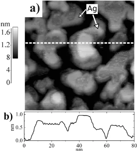
Figure 4. (a) STM image of 0.25 ML Ag deposits on a Pd16M L/Ag/mica
substrate and (b) height profile along the dotted line drawn on the STM image. It= 1.5 nA, Vs = 0.5 V. Lighter areas are attributed to Ag decorating the Pd
terrace tops.
Upon deposition of 0.25 ML of Ag on 16 ML Pd (Fig. 4 (a)) darker areas appear on the top surface of the columns. As shown on the height profile of Fig. 4 (a), the edge around the shaded area has an apparent height of 110 pm. According to ab-initio simulations the edge could be described as Ag atoms in the same layer as the neighboring Pd terraces.
Ag thickness of θ = 0.75 ML
Upon deposition of 0.75 ML of Ag, clusters with a diameter around 1 nm accumulate on top of the columns (Fig. 5 (a)), but do not coalesce. Moreover, they do not nucleate on island tops narrower than 10 nm. The height profile (Fig. 5 (b)) along the horizontal line on the STM image is rather similar to that of Pd16ML/Ag (Fig. 3 (d)) with 3 ML deep grooves between the columns. The oscillations on the central columns are due to the clusters.
Figure 5. (a) STM image of 0.75 ML Ag deposits on a Pd16M L/Ag/mica
substrate and (b) height profile along the dotted line drawn on the STM image. It= 1 nA, Vs = -1.5 V. Small 1nm sized clusters of Ag form on Pd column top
layers, but do not coalesce.
Fig. 6 shows a closer look at an aggregate of clusters on top of a column. The clusters are at the same level as the surface of the columns but appear brighter. As seen on the height profile Fig. 6, the separation between the clusters as well as their width is near 1 nm, while their height is on the order of 0.2 nm. In the following, based on the conclusions of the ab initio calculations on monolayers, we will attribute the bright protrusions on STM images to Ag clusters and stripes, and dark areas to Pd ones.
Due to the relatively higher electrophilicity of Pd, there will be a charge transfer from Ag to Pd. The charge transfer could be responsible for the very high corrugation between Pd and Ag clusters observed in Fig. 6 (150 pm) but it might also be caused by a preferential “chemical” interaction (repulsive or attractive) between the tip and Ag or Pd clusters [34].
Figure 6. (a) STM image of 0.75 ML Ag deposits on a Pd16M L/Ag/mica
substrate and (b) height profile along the dotted line drawn on the STM image. It= 1.5 nA, Vs = -0.015 V. Zoom of Fig. 5 at lower bias voltage.
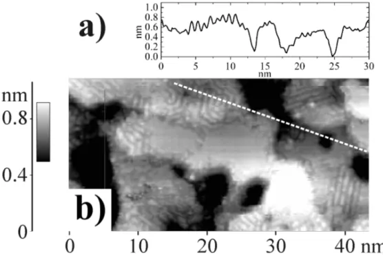
of 0.5-0.7 nm. The patterns follow step edges and make coronas around circular holes, and probably come from Friedel-like oscillations of the electronic density (as in Ref. [32]) – the wavelength corresponds well to those calculated ab initio for a full Ag ML on Pd. Our simulation of Ag1Pd1striped surface alloys have a similar wavelength (0.49 nm) but should be more directional on the (111) surface. From the theoretical discussion above it is clear that the surface must be 1ML Ag on Pd, and can not be pure Pd (several layers of Ag would be improbable given the amount deposited).
Ag thickness of θ ≥ 1 ML
Upon deposition of 1.25 ML of Ag, the surface appears smoother, and deep grooves are less numerous. This trend is confirmed on the image of 3 ML of Ag on Fig. 8: although some 5 ML deep holes still appear, atomically flat terraces extend over more than 80 nm and are separated by monoatomic steps. In addition, between 1 and 3 ML, the surface of some islands is covered by stripes (Fig. 7) growing parallel and stacked in
Figure 7. STM image of 1.25 ML Ag deposits on a Pd16M L/Ag/mica substrate
It= 0.5 nA, Vs = 1. V. a) Line profile along the dotted line in the image b).
domains rotated by 120◦. As seen on the height profile of Fig. 7-b, the distance between the stripes is around 0.9 nm, so about 3 atoms. The stripes seem to be embedded in the surface plane and their height is less than 0.1 nm. Apart from image resolution considerations the presence and the arrangement of the stripes is not affected by the bias voltage between -1.5 and 1.5 V. The ab-initio simulations of 2 atom wide stripes (2 Ag then 2 Pd etc...) are the closest to the spacings seen by STM (1 nm). This case shows very small corrugations, with slightly higher (0.05A) Pd atoms. We attribute the features to alternating Ag and Pd stripes: the wavelength here is clearly larger than that expected for Friedel oscillations.
After deposition of 1.25 to 3 ML the surface becomes smoother. The islands are covered by Ag, and in some cases appear to be bordered by alternating Ag and Pd stripes.
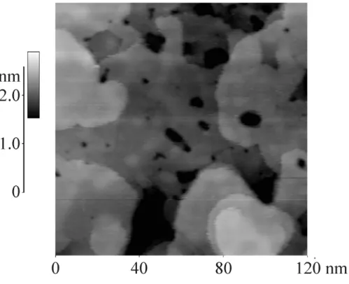
Ag thickness of 3 ML ≤ θ ≤ 10 ML
Terraces of the 3ML Ag/Pd16ML/Ag/mica samples extend over more than 100 nm (Fig. 8). However, their surface is not absolutely flat and maintains a sub-monolayer roughness appearing as lighter and darker regions on the terraces. Approaching the tip closer to the surface by choosing very high current (10 nA instead of 2 nA) for quite low bias voltage (0.1 V, previously around 0.5 V) we could obtain atomically resolved images of the 3 ML of Ag on Pd16ML/Ag. On Fig. 9 (left) a wavy sub-monolayer pattern is observed, often exhibiting triangular shapes. Although this pattern is not periodic,
Figure 8. STM image of 3 ML Ag deposits on a Pd16M L/Ag/mica substrate It= 1
nA, Vs = 0.2 V.
Figure 9. Atom-resolved STM images showing stress release after deposition of 3 ML of Ag on Pd16M L/Ag/mica substrate. It= 10 nA, Vs = 0.1 V. (Left)
Moir´e patterns enhanced by white triangles. (Right) Observation of a triangular dislocation loop arising from stress release.
and is disturbed by step edges and defects, it can be related to a way to release the stress created by the lattice mismatch between Ag and Pd. As the thickness of the
Figure 10. (a) Atom-resolved STM image of 3 ML Ag deposits on a Pd16M L/Ag/mica substrate. Pd atoms appear 80 pm higher than the Ag
lattice. (b) Line profile. It= 10 nA, Vs = 0.1 V.
Ag layer as well as the area of the terraces increase, the energy cost of pseudomorphic growth becomes too high. To bring the interatomic spacing closer to that of bulk Ag, buckling of atoms out of the plane in a triangular pattern occurs. In other regions of the surface, another type of triangle was observed as seen in Fig. 9 (right). In this case the triangles are much better delimited and clearly appear at a lower level than the rest of the surface. These two types of defects have already been observed in other heteroepitaxial systems like Ag/Cu(111) (Ref. [35, 36] and references therein), Co/Pt(111)[37], and Au/Ni(111)[38]. Such superstructures relieve the surface stress due to the lattice mismatch between Ag and Pd. Apart from the intrinsic interest of studying these defects, they show clearly that the Ag is growing pseudomorphically and needs to be relaxed.
As seen in Fig. 10, the presence of some traces of Pd can not be totally excluded. The STM image shows brighter atoms (Pd) having a corrugation about 80 pm higher
than the surrounding Ag atoms. This trend, confirmed by our ab initio is quantitatively comparable to the enhancement of 25 pm observed by Wouda et al.[10] of Pd atoms at the surface of a dilute AgPd alloy.
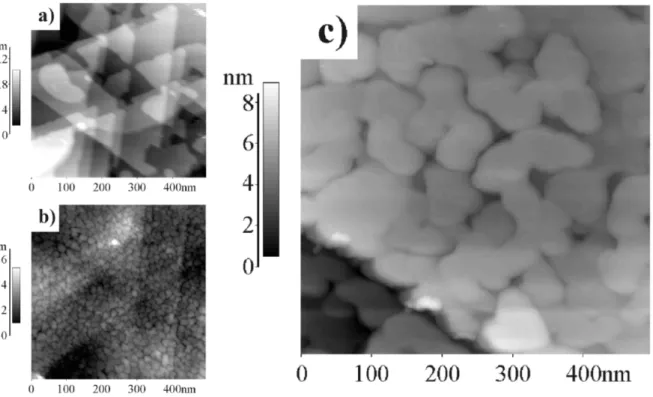
Figure 11. STM image (a) of the bare Ag surface, (b) of Pd16M L/Ag/mica,
with columnar structure, (c) Ag10M L/Pd16M L/Ag/mica, where the Ag overlayer has
induced a subsurface reconstruction, and restored a surface with low roughness.
Fig. 11 shows STM images of the bare Ag/mica, the Pd16M L/Ag/mica and the Ag10M L/Pd16M L/Ag/mica systems. The surface roughness decreases strongly upon increasing the overlayer Ag thickness. Starting with islands having a diameter around 20 nm on the Pd16M L/Ag/mica, we end up, after 10 ML of Ag, with flat terraces extending over hundreds of nanometers, yet still separated by 2 nm deep grooves.
2.3. Growth model Pd growth
In the previous sections, we showed that columnar structures (Fig. 12 (a)) are formed upon deposition of Pd on Ag. This case is similar to the homoepitaxy of Pd(111) and is explained by the high ratio between the step-edge (or Ehrlich-Schwoebel) and the in-plane diffusion barriers on Pd(111), which prevent any downward mass transport during the growth. After deposition of Ag onto this columnar structures, atomically flat surfaces and a two-dimensional growth mode are restored. In this section, we aim to explain how this transition from three- to two-dimensional growth mode is achieved.
Sub-monolayer growth of Ag
Figure 12. schematic representation of the proposed growth mode of Ag (black) on Pd (gray) columns for thickness of 0.25, 0.75 and from 1.25 to 3 ML respectively.
until the whole surface is covered by one monolayer of Ag except for the top Pd layer (Fig. 12 (b-c)). A similar behavior was observed by Trontl[23] in the case of Ag growth on an atomically flat Pd(111) surface. Trontl also showed that Ag was weakly bound to the Pd substrate and followed a layer-by-layer step-flow growth mode thanks to the high mobility of Ag on Pd(111).
In our case, additional Ag does not seem to nucleate on the top (uncovered) Pd layer. Instead, a AgPd mixture constituted of nanometer sized Ag and Pd clusters is formed. Such incomplete mixing has been observed in the heteroepitaxy of Ag on Pt(111)[3] after annealing at 630 K. According to Tersoff et al.[39] such partial mixing results from a balance of the strain energy cost of the 5% misfit of Ag in Pt with the line tension energy of the Ag/Pt boundary length. In addition Massobrio and Blandin[40] showed that Ag clusters of 7, 10 and 12 atoms adsorbed on Pt(111) were particularly stable (the smallest clusters with threefold coordination at the entire cluster perimeter). The AgPd system is very similar to the AgPt system: Ag has a much lower surface energy (1.25 J/m2
) than both Pd (2.05 J/m2
) and Pt (2.48 J/m2
and negative heats of solution make Ag miscible with Pd and Pt. Pd and Pt, being in the same column of the periodic table, have similar electronic structure. Their lattice parameter is also similar (aP d = 389 pm aP t = 392 pm). Finally, Pt and Pd have equal electronegativity and similar workfunctions. Nevertheless, while the partial mixing of Ag with atomically flat Pt and Pd surfaces must be activated by annealing at 630 K and 600 K (respectively in Ref. [3] and [22]), spontaneous mixing occurs at room temperature on the columnar Pd surface.
The additional driving force on the columnar structure is the lack of step edges. On a standard Pd(111) surface, step flow can proceed whatever the thickness of the Ag film, on the columnar Pd structure, step flow ends as soon as the Ag layer reaches the edge of the column. At this point the top surface of the column is constituted by a Pd core and a Ag brim and nucleation of Ag islands should occur on top of the Pd core in order to decrease the surface free energy. Nevertheless, as shown in a previous publication[42] the interface energy between a pseudomorphic Ag layer and Pd is around -90 meV per (111) surface unit cell. Therefore, in order to reduce both the surface and interface energy of the top layer, the incoming Ag atoms progressively exchange places with the top Pd core atoms until a full Ag layer is formed (Fig. 12 (d-e)). Following this mixing/demixing process, the expelled Pd atoms diffuse down the columns thanks to their very high mobility which was already observed for sub-monolayer Pd deposits on the bare Ag(111) surface (Fig. 2) and fill the valleys where they get systematically buried under Ag atoms (Fig. 12 (d-e-f)). Indeed, as shown by Ruban et al.[43], Ag single impurities in a Pd host have a slightly negative segregation energy towards the (111) surface (-0.26 eV/atom) indicating a moderate tendency to segregate towards the surface of AgPd alloys. This argument should not be blindly transposed to the case of concentrated alloys, but Ag enrichment up to 92% has been predicted at the surface of AgPd random alloys at room temperature (due to Ag segregation[8]).
As seen through the observation of striped alloyed phases, the situation is probably more complicated. The final Ag surface is also not perfect and Pd imputities can be found. Nonetheless, the above picture sketches how the Pd columnar structure progressively changes into a flat Ag(111) surface.
Strained Ag growth
For 3 ML thick Ag layers, a strained Ag surface was imaged. This leads to the conclusion that intermixing between the two metals must be very low and thus that the stress cannot be released at the interface. The demixing process that would occur at the completion of the Ag layer in contact with the Pd substrate is thus very effective and leads to a sharp Ag/Pd interface. One should now wonder why the Ag surface that is created is not growing three-dimensionally as is the case for Ag(111) homoepitaxy[16], due to a high Ehrlich-Schwoebel barrier. In fact, the three-dimensional growth observed for Ag and other noble metals is related to the presence of a free-electron like surface state. This surface state decreases the diffusion barrier along terraces by reducing the corrugation of the attractive potential for diffusing adatoms. Moreover, the step-edge barrier increases due to scattering of electrons from this surface state at the step-edge.
The main difference between Ag(111) homoepitaxy and our system is that here Ag is submitted to a compressive strain inducing pseudomorphic growth on Pd as shown by our previous LEED analysis[19]. Similarly to the layer-by-layer growth of up to 6 layers of Ag on Pt(111) observed by R¨oder et al.[44], the main effect of strain is to depopulate the free-electron-like surface state. This depopulation decreases the step-edge barrier and increases the in-plane diffusion barrier, leading to layer-by-layer growth.
3. Conclusions
In the present paper we aimed to explain how the columnar structure obtained from the deposition of Pd on Ag(111) is changed into an atomically flat surface after Ag deposition onto this structure. Various properties of the Ag/Pd system are involved in this transition. First of all Ag and Pd weakly interact with each other. As a result, a high atomic mobility is observed. Ag does not nucleate on top of Pd terraces and aggregates at step edges. Secondly, the interface energy between a pseudomorphic Ag layer and a Pd(111) substrate is relatively large and negative (90 meV per atom). Therefore, partial mixing between Ag and Pd is preferred rather than the nucleation of Ag islands on the top Pd terrace of the columns. This solution reduces the surface free energy of the system without increasing too much the interface energy. Thirdly, the segregation energy of Ag toward the surface of a AgPd alloy is negative. Therefore most of the Pd atoms on the surface are systematically buried under Ag. Finally, two-dimensional growth of Ag(111) is allowed as soon as compressive strain depopulates the free electron like surface states characteristic of most noble metals. The strained Ag layers formed according to the three preceding arguments allow the two-dimensional growth of the following layers. The present work not only explains how Ag/Pd superlattices with sharp interfaces can be formed but also illustrates how the many thermodynamic and kinetic arguments at surfaces may interplay and allow the growth of unexpected structures.
Acknowledgments
The authors have benefited immensely from extended discussions and critical reading by A. Ruban. We also wish to thank Dr. H. Ness for illuminating discussions of STM theory, and H. Brune for encouraging criticism. This work was supported by the Belgian Office for Scientific, Technical and Cultural Affairs (PAI 5.01), by the Belgian National Fund for Scientific Research (FNRS), FRFC projects 2.4556.99, 1.5015.00 F, and 2.4502.05, EC contracts NMP4-CT-2004-500198 (Nanoquanta NoE) and MEIF-CT-2005-024152 (MANET Marie Curie fellowship), and FP6-029192 (DNA Nanodevices). We also thank the Communaut´e Francaise de Belgique for an “Action de Recherche Concert´ee” grant.
[1] K.-O. Ng and D. Vanderbilt. Stability of periodic domain structures in a two-dimensional dipolar model. Phys. Rev. B., 52:2177, 1995.
[2] V. Ozoli¸nˇs, M. Asta, and J.J. Hoyt. Elastic relaxations in ultrathin epitaxial alloy films. Phys. Rev. Lett., 88:096101, 2002.
[3] H. R¨oder, R. Schuster, H. Brune, and K. Kern. Monolayer-confined mixing at the Ag-Pt(111) interface. Phys. Rev. Lett., 71:2086, 1993.
[4] E.D. Tober, R.F.C. Farrow, R.F. Marks, G. Witte, K. Kalki, and D.D. Chambliss. Self-assembled lateral multilayers from thin film alloys of immiscible metals. Phys. Rev. Lett., 81:1897, 1998. [5] T. Marten, O. Hellman, A.V. Ruban, W. Olovsson, C. Kramer, J. Godowski, L. Bech, Z. Li,
J. Onsgaard, and I.A. Abrikosov. Double-segregation effect in AgxPd1-x/Ru(0001) thin film nanostructure. Phys. Rev. B., 77:125406, 2008.
[6] Stefan M¨uller and Alex Zunger. First-principles predictions of yet-unobserved ordered structures in the Ag-Pd phase diagram. Phys. Rev. Lett., 87:165502, 2001.
[7] M. Ropo. Ab-initio study of the geometric dependence of AgPd surface segregation. Phys. Rev. B, 74:195401, 2006.
[8] M. Ropo, K. Kokko, L. Vitos, and J. Kollar. Segregation at the PdAg(111) surface: Electronic structure calculations. Phys. Rev. B, 71:045411, 2005.
[9] A. V. Ruban, S. I. Simak, P. A. Korzhavyi, and B. Johansson. Theoretical investigation of bulk ordering and surface segregation in Ag-Pd and other isoelectornic alloys. Phys. Rev. B, 75:054113, 2007.
[10] P. T. Wouda, M. Schmid, B. E. Nieuwenhuys, and P. Varga. STM study of the (111) and (100) surfaces of PdAg. Surf. Sci., 417:292, 1998.
[11] K. Temst, M. J. Van Bael, C. Van Haesendonck, Y. Bruynseraede, D. G. de Groot, N. Koemann, and R. Griessen. An X-ray diffraction study of interface roughness and diffusion in Ag/Pd superlattices. Thin Solid Films, 342:174–179, 1999.
[12] G.E. Henein and J.E. Hilliard. Interdiffusivities in silver-palladium composition-modulated foils. J. App. Phys, 55:2895, 1984.
[13] G. Gladyszewski. Initial stages of ion-induced interfacial mixing in the Ag-Pd system. Material Letters, 13:287, 1992.
[14] S. Lee, G. Stegeman, J. Kim, C.M. Falco, V. Askarpour, and M. Manghnani. Effect of thermal annealing on elastic properties of Ag/Pd superlattice films. Solid State Communications, 94:691, 1995.
[15] A. Steltenpohl and N. Memmel. Homoepitaxial growth of Pd on Pd(111) - a search for the contribution of electronic surface states to the Ehrlich-Schwoebel barrier. Surf. Sci., 402:277, 1998.
[16] J. Vrijmoeth, H. A. van der Vegt, J. A. Meyer, E. Vlieg, and R. J. Behm. Surfactant-induced layer-by-layer growth of Ag on Ag(111): Origins and side effects. Phys. Rev. Lett., 72:3843, 1994.
[17] G. N. Burland and P. J. Dobson. Pseudomorphic behaviour and interdiffusion between palladium films and silver and gold. Thin Solid Films, 75:383, 1981.
[18] K. H¨aupl and P. Wissmann. X-ray diffraction studies on thin palladium films epitaxially grown on Ag(111). Thin Solid Films, 174:105, 1989.
[19] Jacques Dumont, J. Ghijsen, and R. Sporken. Investigation of the structure of a Ag/Pd/Ag(1 1 1) trilayer by means of electronic spectroscopies. Surf. Sci., 507:234, 2002.
[20] G. C. Smith, C. Norris, C. Binns, and H. A. Padmore. A photoemission study of ultra-thin palladium overlayers on low-index faces of silver. J. Phys. C, 15:6481, 1982.
[21] B. Eisenhut, J. Stober, G. Rangelov, and Th. Fauster. Growth and structure of ag on Pd(111) studied by photoelectron forward scattering using a two-dimensional display-type analyzer. Phys. Rev. B, 47:12980, 1993.
[22] R. Fischer, Th. Fauster, and W. Steinmann. Three-dimensional localization of electrons on Ag islands. Phys. Rev. B, 48:15496, 1993.
[23] V.M. Trontl, I. Pletikosi´c, M. Milun, P. Pervan, P. Lazi´c, D. ˇSokˇcevi´c, and R. Brako. Experimental and ab initio study of the structural and electronic properties of subnanometer thick Ag films
on Pd(111). Phys. Rev. B, 72:235418, 2005.
[24] J. Dumont, J. Ghijsen, F. Wiame, and R. Sporken. Growth of atomically flat Ag on mica. Surf. Sci., 572:459, 2004.
[25] X. Gonze, J.-M. Beuken, R. Caracas, F. Detraux, M. Fuchs, G.-M. Rignanese, L. Sindic, M. Verstraete, G. Zerah, F. Jollet, M. Torrent, A. Roy, M. Mikami, Ph. Ghosez, J.-Y. Raty, and D. C. Allan. First-principles computation of material properties: the abinit software project. Comp. Mat. Sci., 25:478–492, 2002.
[26] N. Troullier and J. L. Martins. Efficient pseudopotentials for plane-wave calculation. Phys. Rev. B, 43:1993, 1991.
[27] John P. Perdew, K Burke, and M Ernzerhof. Generalized gradient approximation made simple. Phys. Rev. Lett., 77:3865, 1996.
[28] J. Tersoff and D. Hamann. Theory and application for the scanning tunneling microscope. Phys. Rev. Lett., 50:1998–2001, 1983.
[29] J. Tersoff and D. Hamann. Theory of the scanning tunneling microscope. Phys. Rev. B, 31:805, 1985.
[30] H. L. Skriver and N. M. Rosengaard. Surface energy and work function of elemental metals. Phys. Rev. B, 46:7157, 1992.
[31] Z. W. Lu, S-H. Wei, and Alex Zunger. Electronic structure of random Ag0.5Pd0.5 and Ag0.5Au0.5
alloys. Phys. Rev. B, 44:10470, 1991.
[32] Y. Hasegawa, Takayuki Suzuki, and T. Sakurai. Modification of electron density in surface states: standing wave observation on Pd overlayers by STM. Surf. Sci., 514:84–88, 2002.
[33] P. Politi and J. Villain. Ehrlich-schwoebel instability in molecular-beam epitaxy: A minimal model. Phys. Rev. B, 54:5114, 1996.
[34] P. Varga and M. Schmidt. Chemical discrimination on atomic level by STM. App. Surf. Sci., 141:287–293, 1999.
[35] C. Mottet, G. Tr´eglia, and B. Legrand. Structures of a ag monolayer deposited on Cu(111), Cu(100), and Cu(110) substrates: An extended tight-binding quenched-molecular-dynamics study. Phys. Rev. B, 46:16018, 1992.
[36] I. Meunier, G. Tr´eglia, J.-M. Gay, B. Aufray, and B. Legrand. Ag/Cu(111) structure revisited through an extended mechanism for stress relaxation. Phys. Rev. B, 59:10910, 1999.
[37] C. Goyhenex and G. Tr´eglia. Theoretical determination of two critical sizes for strain relaxation during Co/Pt(111) heteroepitaxy. Surf. Sci., 446:272, 2000.
[38] J. Jacobsen, L. Pleth Nielsen, F. Besenbacher, I. Stensgaard, E. Laegsgaard, T. Rasmussen, K. W. Jacobsen, and Norskov J. K. Atomic-scale determination of misfit dislocation loops at metal-metal interfaces. Phys. Rev. Lett., 75:489, 1995.
[39] J. Tersoff. Surface-confined alloy formation in immiscible systems. Phys. Rev. Lett., 74:434, 1995. [40] C. Massobrio and P. Blandin. Structure and dynamics of Ag clusters on Pt(111). Phys. Rev. B,
47:13687, 1993.
[41] W. R. Tyson and W. A. Miller. Surface free energies of solid metals: Estimation from liquid surface tension measurements. Surf. Sci., 62:267–276, 1977.
[42] Matthieu Verstraete, J. Dumont, R. Sporken, R. L. Johnson, F. Wiame, K. Temst, J. Swerts, F. Mirabella, J. Ghijsen, and Xavier Gonze. Structural and electronic properties of Ag-Pd superlattices. Phys. Rev. B, 70:205427, 2004.
[43] A. V. Ruban, H. L. Skriver, and J. K. Norskov. Surface segregation energies in transition-metal alloys. Phys. Rev. B, 59:15990, 1999.
[44] H. R¨oder, K. Bromann, H. Brune, and K. Kern. Strain mediated two-dimensional growth kinetics in metal heteroepitaxy: Ag/Pt(111). Surf. Sci., 376:13, 1997.