HAL Id: hal-01069414
https://hal.archives-ouvertes.fr/hal-01069414
Submitted on 29 Sep 2014
HAL is a multi-disciplinary open access
archive for the deposit and dissemination of
sci-entific research documents, whether they are
pub-lished or not. The documents may come from
teaching and research institutions in France or
abroad, or from public or private research centers.
L’archive ouverte pluridisciplinaire HAL, est
destinée au dépôt et à la diffusion de documents
scientifiques de niveau recherche, publiés ou non,
émanant des établissements d’enseignement et de
recherche français ou étrangers, des laboratoires
publics ou privés.
All-optical signal processing using silicon devices
Leif Katsuo Oxenløwe, Minhao Pu, Yunhong Ding, Hao Hu, Francesco da
Ros, Dragana Vukovic, Asger Sellerup Jensen, Hua Ji, Michael Galili,
Christophe Peucheret, et al.
To cite this version:
Leif Katsuo Oxenløwe, Minhao Pu, Yunhong Ding, Hao Hu, Francesco da Ros, et al.. All-optical
signal processing using silicon devices. 40th European Conference on Optical Communication (ECOC
2014), Sep 2014, Cannes, France. pp.We.2.5.1, �10.1109/ECOC.2014.6964241�. �hal-01069414�
ECOC 2014, Cannes - France
We.2.5.1
All-Optical Signal Processing using Silicon Devices
L.K. Oxenløwe
(1), M. Pu
(1), Y. Ding
(1), H. Hu
(1), F. Da Ros
(1), D. Vukovic
(1), A. Sellerup Jensen
(1), H. Ji
(1),
M. Galili
(1), C. Peucheret
(2), K. Yvind
(1)(1)
DTU Fotonik, Ørsteds Plads 343, Kgs. Lyngby, Denmark,
[email protected]
(2)
FOTON Laboratory, CNRS UMR 6082, ENSSAT, University of Rennes 1, 22305 Lannion, France
Abstract This paper presents an overview of recent work on the use of silicon waveguides for
processing optical data signals. We will describe ultra-fast, ultra-broadband, polarisation-insensitive and
phase-sensitive applications including processing of spectrally-efficient data formats and optical phase
regeneration.
Introduction and background
As the Internet traffic maintains its double-digit
percentage growth, the need for novel and more
energy- and spectrally efficient processing
technologies never subsides. With the (re-)
introduction of coherent communications and
advanced modulation formats strongly bound to
electronic digital signal processing (DSP), a
whole range of transmission impairment
mitigation techniques have become possible.
These
include
in
particular
dispersion
compensation, and to some degree nonlinear
transmission impairment compensation by e.g.
digital back-propagation
1. Alongside these very
successful DSP endeavours, optical signal
processing (OSP) has been undergoing a
tremendous development, though still short of
commercial penetration. Over recent years, OSP
has been demonstrated to allow for
phase-sensitive amplification for phase regeneration
2,
ultra-broadband flexi-grid light sources
3,
add/drop multiplexing of spectrally intertwined
data channels like OFDM
4, time lens based
linear transmission impairment compensation
5,
optical phase conjugation and optical twin-wave
transmission
for
nonlinear
transmission
impairment compensation
6-7, and many other
exciting functionalities. The foundation of OSP is
efficient optical nonlinearities, and many
materials are being investigated today. The most
successful
materials
platform
today
is
undoubtedly highly nonlinear fibres (HNLF),
where the nonlinearity may be accumulated over
a large length of fibre. HNLF, however, needs
special efforts to reduce stimulated Brillouin
scattering and increase the OSP bandwidth,
which may be improved on by Al-doping, strain
and stable dispersion designs like the
SPINE-HNLF
8. Compact waveguide platforms are also
very interesting, in particular because of the very
stable dispersion properties, allowing for
ultra-broadband OSP bandwidths, as demonstrated
e.g. in silicon nanowires
9. Other platforms
include chalcogenide (ChG) waveguides
10, III-V
photonic wires
11, periodically poled Lithium
Niobate (PPLN)
12and semiconductor optical
amplifiers (SOAs)
13. This paper will focus on
silicon optical signal processing and mostly on
crystalline
silicon
(c-Si).
However,
c-Si
waveguides suffer from two-photon absorption
(TPA) at 1550 nm, and hence other related
materials are heavily researched today—such as
amorphous silicon
14with reduced TPA allowing
for more efficient lower power OSP
15-18, as well
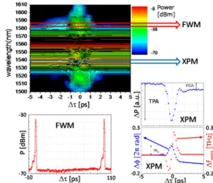
Fig. 1: Ultra-fast FWM and XPM in a silicon nanowire 24
Fig. 2: Ultra-broadband FWM bandwidth available with
dispersion-engineered silicon nanowire. Lower right: Example of FWM-based broadband OSP: Wavelength
conversion, up to 640 Gbit/s 26-28.
ECOC 2014, Cannes - France
We.2.5.1
as Hydex glass and silicon nitride
19-21, as well as
III-V wires
11. One other approach is to apply a
p-i-n junction across ones wire and apply a reverse
voltage to reduce the steady state density of free
carriers, thus strongly reducing the nonlinear
absorption loss
22-23.
Ultra-fast and ultra-broadband OSP in c-Si
Fig. 1 shows an experimental spectrogram
24of a
pump-probe characterisation in a c-Si nanowire.
This shows that there is indeed no memory effect
in FWM in c-Si, and that XPM has both a fast red
and fast blue shift, allowing for dual-copy
wavelength conversion
25. Fig. 2 shows how
proper
nano-engineering
by
waveguide
dimensioning can match
2and
4to yield an
ultra-broadband FWM bandwidth extending over
several hundred nm
26-
27. Thus c-Si nanowires
may be used for both fast and
ultra-broadband OSP. Fig. 2 also shows an example
of ultra-fast wavelength conversion of an up to
640 Gbit/s serial data signal
28. Other broadband
demonstrations include 640 Gbit/s
serial-to-parallel conversion
29, OSP of 1.28 Tbit/s data
30,
BER-confirmed OOK all-optical regeneration
31-33], Fig. 3 shows a very recent experiment, where
wavelength conversion of the very spectrally
efficient data format Nyquist-OTDM was
demonstrated at 320 Gbit/s
34.
Polarisation-insensitive OSP in c-Si
All the above functionalities are based on
polarisation sensitive processes, so it is very
important
to
find
polarisation-insensitive
solutions. Fig. 4 shows an integrated
polarisation-diversity chip using two c-Si nanowires with a
polarisation splitter and rotator (PSR) in either
end
35. An integrated polarisation-insensitive
optical ring resonator based DPSK demodulator
was implemented in a similar way
36. In
35, as
shown in Fig. 4, 40 Gbit/s
polarisation-independent optical phase conjugation was
accomplished allowing for 160 km transmission.
Other similar approaches are demonstrated in
SOAs
37and PPLN
38.
Phase-sensitive amplification in c-Si
Fig. 5 shows results from
39with the first
phase-regeneration using silicon. A c-Si nanowire in a
p-i-n junction
22is employed to reduce
accumulation of TPA-generated free carriers.
With this device it is possible to increase the
pump power and use longer waveguides (4 cm)
enabling a very high CW conversion efficiency of
minus a few dB with -25 V bias
40. This high
efficiency enable a phase-sensitive extinction
ratio (ER) up to a record 20 dB for a chip with CW
operation, and this in turn allows for a
demonstration of 10 Gbit/s DPSK phase
regeneration with a 14 dB receiver sensitivity
improvement. Other chip-based investigations
count Si photonic crystal waveguides with 11 dB
ER
41, ChG
42and PPLN
43.
Conclusions
We have attempted to provide an overview of
major milestones achieved using crystalline
silicon nanowires for optical signal processing.
Nanowires have the benefit of allowing for
ultra-fast and ultra-broadband OSP, and may in
addition be made polarisation-independent and
with very high conversion efficiency allowing for
phase-sensitive applications.
Fig. 4: Polarisation-insensitive FWM device with integrated silicon nanowires 35.
Fig. 3: Ultra-fast FWM-based wavelength conversion of
a 320 Gbit/s Nyquist-OTDM data signal 34.
Acknowledgements
A. Gajda, L.
Zimmermann, B. Tillack,
K. Petermann for Si
p-i-n collaboratiop-i-n, ERC
SOCRATES, VKR
NATEC, FTP NESTOR,
FTP Terabit on Silicon,
FTP SiMOF.
Page 2/3ECOC 2014, Cannes - France
We.2.5.1
References
[1] E. Ip et al, “Compensation of dispersion and nonlinear impairments using digital back propagation,” J. Lightwave Technol. 26, 3416–3425 (2008)
[2] R. Slavik et al, “All-optical phase and amplitude regenerator for next-generation telecommunications systems,” Nat. Photonics 4, 690–695 (2010).
[3] A. Vahid et al, Flex-grid Compatible Ultra Wide Frequency Comb Source for 31.8 Tb/s Coherent Transmission of 1520 UDWDM Channels, OFC 2014, Th5B.7
[4] T. Richter et al, ” Coherent In-line Substitution of OFDM Subcarriers Using Fiber-Frequency Conversion and Free-Running Lasers”, OFC 2014, paper Th5B.6 [5] M. Nakazawa et al, “Ideal distortion-free transmission
using optical Fourier transformation and Fourier transform-limited optical pulses,” Photon. Technol. Lett., Vol. 16, No. 4, pp. 1059-1061, 2004.
[6] H. Hu et al, Fiber Nonlinearity Compensation of an 8-channel WDM PDM-QPSK Signal using Multiple Phase Conjugations, OFC 2014, paper M3C.2
[7] X. Liu et al, “Phase-conjugated twin waves for communication beyond the Kerr nonlinearity limit,” Nature Photon. 7, 560-568 (2013).
[8] http://ofscatalog.specialtyphotonics.com
[9] N. Ophir et al, "Wavelength conversion and unicast of 10-Gb/s data spanning up to 700 nm using a silicon nanowaveguide." Opt. Express, Vol. 20, No. 6, (2012). [10] B.J. Eggleton et al, Chalcogenide Photonics, Nature
Photonics 5, 141-148, doi:10.1038/nphoton.2011.309 [11] J.J. Wathen, “Efficient continuous-wave four-wave mixing
in bandgap-engineered AlGaAs waveguides” Optics Letters, Vol. 39, No. 11 (2014)
[12] A. Bogoni et al, “640 Gb/s all-optical regenerator based on a periodically poled Lithium Niobate waveguide,” J. Lightwave Technol., Vol. 30, No. 12, pp. 1829-1834, 2012 [13] H. C. H. Mulvad et al, “640 Gbit/s OTDM lab-transmission and 320 Gbit/s field-transmission with SOA based clock recovery,” OFC 2008, paper OWS2, 2008.
[14] B. Kuyken et al, “Nonlinear properties of and nonlinear
processing in hydrogenated amorphous silicon
waveguides,” Opt. Express., Vol. 19, No. 26, 2011. [15] K-Y Wang et al, Ultralow power continuous-wave
frequency conversion in hydrogenated amorphous silicon waveguides, Optics Lett., Vol. 37, No. 8 (2012) [16] K-Y Wang et al, ultralow-power all-optical processing of
high-speed data signals in deposited silicon waveguides, Optics Express, vol 20, no 22, (2012)
[17] S. Suda et al, Pattern-effect-free all-optical wavelength conversion using a hydrogenated amorphous silicon waveguide with ultra-fast …, Opt. Lett., 37(8) (2012)
[18] C. Grillet et al, amorphous silicon nanowires combining high nonlinearity, FOM and optical stability, Optics Express, vol 20, no 20, (2012)
[19] D.J. Moss et al, New CMOS-compatible platforms based on silicon nitride and Hydex fro nonlinear optics, NPHOT, DOI: 10.1038/NPHOTON.2013.183
[20] Y. Okawachi et al, Octave-spanning frequency comb generation in a silicon nitride chip, Opt. Lett., 36(17) 2011 [21] J. F. Bauters et al, “Ultra-low-loss high-aspect-ratio Si3N4
waveguides,” Opt. Express 19(4), 3163–3174 (2011) [22] A. Gajda et al, “Highly efficient CW parametric conversion
at 1550 nm in SOI waveguides by reverse biased p-i-n junction,” Opt. Express 20, 13100–13107 (2012). [23] R. Jones et al, Net continuous wave optical gain in a low
loss silicon-on-insulator waveguide by stimulated Raman scattering, Optics Express, ol 13, no 2, (2005)
[24] M. Ma et al, “Detailed time-resolved spectral analysis of ultra-fast four-wave mixing in silicon nanowires,” Proc IPC 2011, paper TuV2, 2011.
[25] H. Ji et al, “Two-copy wavelength conversion of an 80 Gbit/s serial data signal using cross-phase modulation in
a silicon nanowire and detailed pump-probe
characterisation” ECOC 2012, Paper We.2.E.3. [26] H. Hu et al, “Ultra-high-speed wavelength conversion in a
silicon photonic chip,” Opt. Exp., 19(21), 2011.
[27] M. Pu et al, “15-THz tunable wavelength conversion of picosecond pulses in a silicon waveguide.” IEEE Photonics Technology Letters, vol. 23, no. 19, 2011. [28] H. Hu et al, “Silicon Chip based Wavelength Conversion
of Ultra‐High Repetition Rate Data Signals”, OFC 2011, postdeadline paper PDPA8
[29] H. C. Hansen Mulvad et al, “Ultra-high-speed optical serial-to-parallel data conversion in a silicon nanowire,” ECOC' 2011, Paper Th.13.A.2 (postdeadline paper) [30] L.K. Oxenløwe et al, ”Silicon Photonics for Signal
Processing of Tbit/s serial data signals”, IEEE J. Select. Topics Quantum Electron., Special Issue, vol 18 no 2, pp996-1005, March/April 2012 (invited paper)
[31] H. Ji et al, “40 Gbit/s serial data signal regeneration using self-phase modulation in a silicon nanowire,” IPC 2012, paper ThQ1
[32] A. S. Jensen et al,” All-optical 40 Gbit/s regenerative wavelength conversion based on cross-phase modulation in a silicon nanowire”, OECC 2013, 2013. Paper ThM1-2. [33] R. Salem et al, “Signal regeneration using low-power
four-wave mixing on silicon chip,” Nature Photonics 2, 2008. [34] A. S. Jensen et al, ” Wavelength Conversion of a
320-Gbit/s Nyquist DPSK Signal using Four-Wave Mixing in a Silicon Nanowire” submitted
[35] D. Vukovic et al, Polarization-insensitive wavelength conversion of 40 Gb/s NRZ-DPSK signals in a silicon polarization diversity circuit, Opt. Express, 22(10), (2014) [36] Y. Ding et al, “Polarization diversity DPSK demodulator
on the silicon-on-insulator platform with simple fabrication,” Opt. Express 21(6), 7828–7834 (2013). [37] C. M. Gallep et al, “Polarization independent dual
wavelength converter based on FWM in a single semiconductor optical amplifier,” OFC 2010, OWP2. [38] I. Brener et al, “Polarisation-insensitive wavelength
converter based on cascaded nonlinearities in LiNbO3 waveguides,” Electron. Lett. 36(1), 66–67 (2000). [39] F. da Ros et al, Phase regeneration of DPSK signals in a
silicon waveguide with reverse biased p-i-n junction, Optics Express, vol 22, no 5 (2014)
[40] F. Da Ros et al, “Continuous wave phasesensitive four-wave mixing in silicon four-waveguides with reverse-biased p-i-n junctions,” ECOC 2013, paper P.2.11
[41] Y. Zhang et al, “Phase-sensitive amplification in silicon photonic crystal waveguides,” Opt. Lett. 39, (2014). [42] R. Neo et al, “Phase-sensitive amplification of light in a
χ(3) photonic chip using a dispersion engineered chalcogenide ridge waveguide,” Opt.Express 21, (2013) [43] B. J. Puttnam et al, “Large phase sensitive gain in
periodically poled lithiumniobate with high pump power,” IEEE Photon. Technol. Lett. 23, 426–428 (2011).
Fig. 5: Phase-regeneration in a crystalline silicon
nanowire in a p-i-n junction39.
-46 -44 -42 -40 -38 -36 -34 -32 -30 -28 11 10 9 8 7 6 5 4 3 2
Before After reg. No noise 4 GHz noise 5 GHz noise 6 GHz noise -l og( BER ) Prec (dBm) w/ o no is e w/ noi se Powered by TCPDF (www.tcpdf.org) Page 3/3