HAL Id: hal-02880855
https://hal.sorbonne-universite.fr/hal-02880855
Submitted on 8 Jan 2021HAL is a multi-disciplinary open access archive for the deposit and dissemination of sci-entific research documents, whether they are pub-lished or not. The documents may come from teaching and research institutions in France or abroad, or from public or private research centers.
L’archive ouverte pluridisciplinaire HAL, est destinée au dépôt et à la diffusion de documents scientifiques de niveau recherche, publiés ou non, émanant des établissements d’enseignement et de recherche français ou étrangers, des laboratoires publics ou privés.
Impedance Spectroscopy Analysis of Structural Defects
in Sputtered ZnO Films
Josiane Soares Costa, Michel Prestat, Bernard Tribollet, Benoit Lescop,
Stéphane Rioual, Lorenz Holzer, Dominique Thierry
To cite this version:
Josiane Soares Costa, Michel Prestat, Bernard Tribollet, Benoit Lescop, Stéphane Rioual, et al.. Impedance Spectroscopy Analysis of Structural Defects in Sputtered ZnO Films. ChemElectroChem, Weinheim : Wiley-VCH, 2020, 7 (9), pp.2055-2064. �10.1002/celc.202000087�. �hal-02880855�
1
Impedance spectroscopy analysis of structural defects in sputtered ZnO films
J. Soares Costa a,b, M. Prestat a*, B. Tribollet c, B. Lescop b, S. Rioual b, L. Holzer d, D. Thierry a
a French Corrosion Institute, 220 rue Pierre Rivoalon, 29200 Brest, France. b Univ Brest, Lab-STICC, CNRS, UMR 6285, 29200 Brest, France.
c Sorbonne Université, CNRS, Laboratoire Interfaces et Systèmes Electrochimiques, LISE,
75005 Paris, France.
d Institute of Computational Physics, Zurich University of Applied Sciences, Wildbachstrasse
21, 8400 Winterthur, Switzerland.
* corresponding author, e-mail: michel.prestat@institut-corrosion.fr
Abstract
The degradation of sputtered columnar ZnO layers under DC polarization was studied by electrochemical impedance spectroscopy and electron microscopy. It was found that the structure of the as-deposited ZnO film was dense at the nanoscale. An equivalent circuit model including a de Levie impedance accounted for the localized propagation of microscaled cracks towards the copper substrate. This generates a capacitance (CZnO) that represents the crack
surface area in contact with the electrolyte. CZnO is small enough not to be obscured by the
double layer capacitance at the top of the layers and increases with increasingly negative potential and time. These results were compared to nanoporous ZnO layers that behave differently and exhibit a large CZnO. The combination of in situ EIS analysis with the ex situ
structural information provided by electron microscopy proved to be an efficient methodology to characterize very different microstructures of conductive coatings.
Keywords: impedance spectroscopy, microstructure, thin films, sputtering, zinc oxide.
1. Introduction
One of the most common strategies to protect metals from corrosion due to aggressive environments is to apply a coating on its surface. The coating acts as a physical barrier and may also provide galvanic protection in defect areas (as in the well-known case of galvanized steel). Eventually the protective properties decays. Thus, there is a prime interest in developing methodologies that enable to characterize, monitor and gain understanding in the degradation mechanism of those coatings. Regarding the decrease of the barrier properties, focus should be
2
laid on the evolution of the microstructure of the layers and the development of defects, such as pores or cracks. Electrochemical impedance spectroscopy (EIS) can bring valuable insights in that matter provided that the equivalent circuits used for data analysis carry a truly physical meaning [1]. For instance, EIS has already been used by Barres et al. to investigate the porosity of silicon nitride (SiNx) thin films (30-60 nm) used in the glass industry as barrier layers [2].
In this work, high-resolution electron microscopy analysis revealed the presence of nanoscale pores (0.5 - 2 nm). The study distinguished “through-pores” in which the electrolyte could reach an underlying gold substrate and “non-through-pores” that crossed only a portion of SiNx
layer. The impedance of the former was modelled as a pore resistance in series with a CPE with the distribution of resistivity of the latter being accounted for with the Young model [3,4]. The de Levie model has been developed for “ideal” electrodes exhibiting high electrical conductivity (“metallic electrodes”) and parallel cylindrical pores with identical geometry to describe frequency dispersion using transmission lines [5]. Several studies showed that the de Levie impedance could be used to describe analytically more complex systems with pores of various geometry, length and radius [6-9]. Barcia et al. utilized the de Levie impedance to characterize macroporous red rust of cast iron in Evian mineral water [9].
In the present work, EIS measurements were performed to gain more understanding about the structural degradation of “model” ZnO layers in alkaline electrolyte. The results of columnar ZnO layers, that are compact at the nanoscale, are compared with those of nano-granular ZnO exhibiting a nanoporous structure. The ZnO electrodes were prepared by radio-frequency magnetron sputtering. This deposition technique conveniently enables to prepare layers of various nanostructures by modifying experimental parameters, such as type of target, power, substrate temperature, and fluxes of reactive gases [10-13]. The experimental impedance data was fitted with two equivalent circuit models, one accounting for a fully dense ZnO layer and the other describing the penetration of the electrolyte in the defects of the films. The global in situ information provided by EIS was completed by the local ex situ structural data at the nanoscale and microscale obtained with top-view and cross-sectional electron microscopy images. In the past years, some reports have demonstrated the benefits of cross-sectional analysis (with focus ion beam or scanning transmission electron microscopy) in order to gain valuable insight on the effect of the microstructure on the protective properties of ZnO [14-19]. A negative polarization was applied to the sputtered ZnO electrodes since the present study was carried out in the context of the investigation of the cathodic properties of ZnO [14-16,21]. The cathodic activity of ZnO is still debated in the literature [14-16, 20-23], as reminded by
3
Cole in a recent review on zinc corrosion [24]. A previous work of our group presented the electrokinetic properties of sputtered ZnO layers towards oxygen reduction [16].
Experimental
Synthesis of the ZnO layers
ZnO films were deposited on copper substrates by radio-frequency magnetron sputtering (Univex 350, Oerlikon). Copper cylinder substrates (5 mm diameter, 4 mm height) were micro-machined from commercially available rods (purity > 99.95%, GoodFellow) to fit the rotating disk electrode setup. After machining, the substrates were grinded with SiC paper (P2500 and P4000 for 60 s each) using water as a lubricant. The finishing of the surface was done with a polishing cloth and polycrystalline diamond suspensions (3 μm and 1 μm, each for 180 s). The substrates were then ultrasonically cleaned in ethanol, rinsed in deionized water and air-dried. For sputtering deposition of the columnar ZnO films, the working chamber was vacuumed to reach a base pressure of 3-5 10-7 mbar. The substrates were fixed at a distance of ca. 10 cm parallel to the ZnO target surface (diameter: 3 inches). Films were deposited for 90 minutes with a mixture of reactive gas (Argon: O2, 15:10 sccm) inside the chamber. The gas purities
were 99.9996% for Argon and 99.9995% for O2. Pre-sputtering was carried out for 30 min to
clean and equilibrate the target surface prior to deposition. The same conditions were used for pre-sputtering and sputtering, except deposition time. During deposition, the total pressure was kept at 2 x10⁻² mbar. The input power at the target was 75 W. The resulting layers were ca. 300 nm thick.
For the synthesis of nano-granular ZnO layers, a zinc target (diameter: 3 inches) was used. The mixture of argon and oxygen gases was Ar:O2 20:3 sccm. The total pressure was 1.7 x10⁻² mbar
and the input power 250 W. The layers had a thickness of ca. 800 nm for a deposition time of 5 min.
Characterization
X-ray diffraction (XRD) was carried out to evidence the crystalline structure of the ZnO layers using PANalytical Empyrean apparatus with CuK radiation (1.5408 Å).
High-angle annular dark-field scanning transmission electron microscopy (HAADF-STEM) imaging was used to characterize the internal structure of the as-deposited layers at the nanoscale and notably its degree of compacity based on Z-contrast. For this purpose, TEM-lamellas representing cross-sections of the ZnO layers were prepared with the focused ion beam
4
(FIB) technique. The ZnO layers were then investigated with an analytical TEM (FEI Talos F200X) at 200 kV.
Top-view imaging was performed by conventional scanning electron microscopy (SEM, SU3500, Hitachi) to evaluate the aspect of surface of the layers at the microscale. The Zn:O ratio was determined by energy dispersive X-ray spectroscopy (EDX, UltraDry EDX detector and Thermo Scientific software NSS 312) with an acceleration voltage of 5 kV.
Electrochemical measurements
The electrochemical experiments were conducted at room temperature in aerated KOH solutions at pH = 10 +/- 0.1 with KCl 0.2 M as supporting electrolyte. EIS measurements were carried out under controlled hydrodynamic conditions using the rotating disk electrode (RDE) technique (Pine Research Instrumentation, Durham, NC, USA). The counter-electrode was a large titanium-based metallic grid placed below the working electrode. The reference electrode was a mercury/mercury oxide electrode (Hg-HgO, KOH 1M). The three-electrode setup was controlled by a Gamry Reference 600 potentiostat. The applied frequency domain ranged from 105 Hz to 1 Hz with 10 points per decade. The sinusoidal perturbation was 10 mV. Data fitting was carried out using non-commercial software developed at the Laboratoire Interfaces et Systèmes Électrochimiques (LISE), Paris, France.
In preliminary measurements in air between two copper electrodes (not shown here), both types of ZnO exhibited sufficiently high electrical conductivity (around 10-2 Ω-1 cm-1). This enabled to neglect the ohmic drop within the ZnO layers during DC polarization. In potentiodynamic voltammetry experiments, the cathodic polarization curves were recorded with a scan rate of 1 mV/s.
2. Results and discussion
Figure 1 shows the XRD patterns of the ZnO thin films. For the layers prepared with the zinc oxide target, the presence of a strong (002) peak at 34° indicates a clear preferred orientation along the c-axis of the wurtzite structure (although a minor diffraction peak at 62.7° associated with (013) planes is observed). This finding is in good agreement with the results reported in the literature using similar conditions as in the present work [25-29]. In contrast, the diffractogram of the samples prepared with the zinc target exhibit multiple peaks, such as (002), (010) and (011), which characterizes the absence of preferred orientation.
The atomic composition of the films was measured by EDX (not shown here) confirming the deposition of ZnO with a Zn:O ratio close to 1:1 for both types of films.
5
Electron microscopy analysis provides relevant ex situ microstructural information on the ZnO layers at the microscale and the nanoscale. Analysis of HAADF-STEM images allows determining porosity (that appears in black contrast) at the nanoscale [2,30,31]. The columnar ZnO (prepared with ZnO target) is evidenced to have a very compact structure (Figure 2a).
Figure 1: XRD spectra of the as-deposited ZnO thin films: columnar ZnO prepared with ZnO target (red curve) and nano-granular ZnO deposited using a Zn target (black curve).
6
Figure 2: HAADF-STEM analysis of the as-deposited ZnO layers: (a) columnar ZnO and (b) nano-granular ZnO.
Only very thin vertical black lines between the columns were detected. They are interpreted either as grain boundaries or as extremely narrow pores that are very unlikely to let the electrolyte go through in view of their aspect ratio. The width of the columns is ca. 30-100 nm. Figure 2b demonstrates that the nano-granular ZnO (prepared with Zn target) has a nanoporous structure. The HAADF-STEM observations are therefore consistent with the XRD findings of Figure 1.
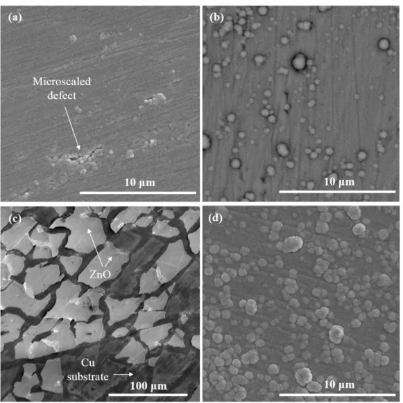
Figure 3: Top-view SEM micrographs of the two types of ZnO layers in the as-deposited state and after polarization at -0.7 V. (a) as-deposited columnar ZnO; (b) as-deposited nano-granular ZnO; (c) columnar ZnO after polarization; (d) nano-granular ZnO after polarization.
7
Figure 3 shows the surface of the ZnO films using conventional SEM, providing therefore relevant morphological information at the microscale. The micrographs were taken in the as-deposited state and after cathodic polarization at -0.7 V. The open circuit potential (OCP) was ca. -0.05 to -0.1 V, depending on the sample. For the columnar ZnO, one can notice the presence of some micro-scaled defects in the otherwise dense microstructure (Figure 3a). After polarization at -0.7 V, the films are cracked and partially delaminated (Figure 3c). The degree of damage after polarization varied from one sample to another. Cracks were systematically present but their number varied. This mechanical instability does not affect the nano-granular ZnO that only becomes rougher under polarization by developing some nodule-like features at its surface (Figure 3b and 3c).
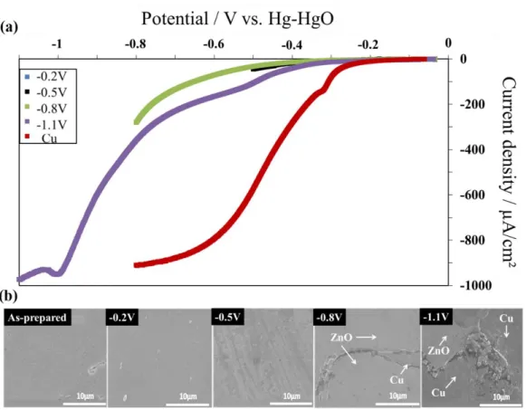
Figure 4: DC characterization of two typical columnar ZnO samples: (a) Polarization curves between open-circuit potential (ca. -0.05 V) and various increasingly negative potentials: -0.2 V, -0.5 V, -0.8 V and -1.1 V (in this order). The polarization curve of bare copper (red curve) is also displayed for comparison. For all curves, the disk potential scan rate was 1 mV s-1 and the rotation rate was 1000 rpm.
8
The typical DC behaviour of a columnar ZnO film is displayed in Figure 4. Figure 4a shows the polarization curves of a single ZnO layer recorded between open circuit potential and various end-potentials: -0.2 V, - 0.5 V, -0.8 V and -1.1 V, in this order. After each polarization, the ZnO film surface was investigated by SEM to search for degradation evidence (Fig. 4b). The curve of the copper substrate is also provided for comparison. A significant difference of activity between ZnO and copper is observed. At -0.6 V, the current density obtained for ZnO was ca. -100 μA/cm2 while that of copper was ca. -900 μA/cm2. This result shows that this type
of ZnO is not an efficient ORR electrocatalyst. Furthermore the electrochemical behaviour of columnar ZnO was found to be unstable.
When the potential scan was stopped at -0.2 V and -0.5 V, the polarization curves remained unchanged. Though a slight roughening of the surface is visible at -0.5 V (Figure 4b), no significant damage, such as cracks, was detected. After the polarization till -0.8 V, large cracks were visible, leading in some cases to local delamination of the ZnO films. Typically, during potentiodynamic experiments, partial rupture of the film is observed at potential around -0.6 V, though the rupture potential and the degree of damage might vary from one sample to another. At the beginning of the fourth experiment (polarization till -1.1 V), the film was already damaged and exposed the underlying copper substrate. This explains the higher current density in the polarization curve. The consequence of the relatively fast mechanical instability of the columnar ZnO films is that in-depth investigation of the oxygen reduction mechanism and kinetics using collection-based techniques, such as rotating-ring disk electrode (RRDE) or double channel flow cell [22,32,33], was not possible. A recent RRDE study of ORR on the more stable nano-granular ZnO is available elsewhere [16].
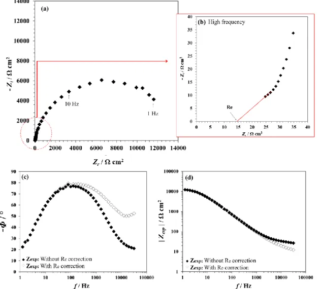
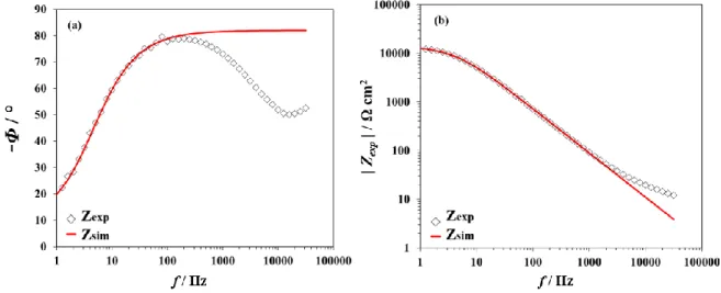
DC polarization curves coupled with post-mortem top-view SEM analysis evidence the potential dependence of the degradation. However, this approach does not provide significant insights on the initial stages of the degradation. Hence EIS experiments were also performed to gain more understanding on this process. Note that, in what follows, resistance, impedance and capacitance values are expressed relative to the geometrical surface area of the disk electrode (i.e. in Ω cm2 and in μF/cm2). Figure 5 shows the experimental impedance, Zexp, of
the columnar ZnO (real part: Zr ; imaginary part: Zi).
It has been demonstrated in the literature that, in the “classical” Bode plots (as-recorded, without correction), the high frequency data might be obscured by the electrolyte resistance, Re , which can be misleading for data interpretation [34-36]. In the present study, the Re value
9
frequencies (Figs. 5a and 5b). The effect of the Re correction on the Bode plots is shown in
Figs. 5c and 5d.
Figure 5: Typical EIS diagrams for columnar ZnO (recorded at -0.4V). (a) Nyquist plot with (b) zoom in high frequency to determine the electrolyte resistance (Re). Bode plots (without and with Re
correction): (c) phase curve and (d) modulus curve.
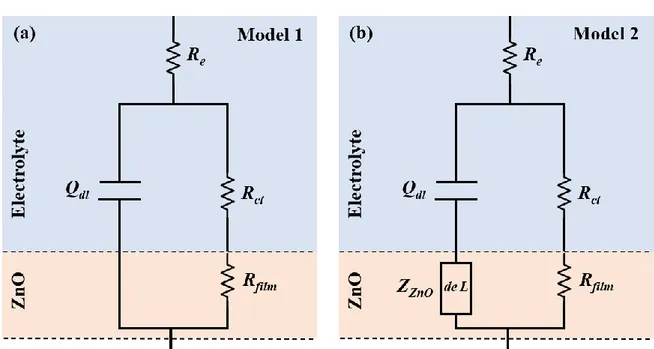
Two equivalent circuit models were tested for describing the AC behaviour of the ZnO films under cathodic polarization (Figure 6). Model 1 describes a fully dense ZnO layer (Figure 6a) whereas Model 2 includes a de Levie impedance (hereafter denoted ZZnO) to account for the
penetration of the electrolyte in the structural defects of the films, such as cracks and pores (Figure 6b). The components of the models are described in the next lines.
10
Re is the electrolyte resistance between the ZnO film and the reference electrode. The faradaic
impedance, Zf, is simplified to a cathodic charge transfer resistance, Rct . An anodic contribution
is not necessary as the EIS measurements are carried out at negative overpotentials “far” from the OCP. Thus:
Zf = Rct (1)
Figure 6: Equivalent circuit models: (a) Model 1 describing a fully dense ZnO layer (without de Levie impedance); (b) Model 2 with de Levie impedance accounting for a ZnO layer with microstructural defects (cracks, porosity).
Rfilm is the electronic resistance of the film. As mentioned above, the resistivity ρ was evaluated
to be ca. 102 Ω cm for both types of ZnO. This low resistivity value suggests that the impedance of the ZnO layers cannot be described by models accounting for distribution of resistivity within the films (such as the Young model [3] or the power law model [4]). Rfilm equals the
product L (with L being the layer thickness of ca. 300 nm or 800 nm) and is around ~ 3 - 8 10-3 Ω cm2. Rfilm is much smaller than Rct and is therefore neglected in the fitting process for
both Model 1 and Model 2.
The double layer capacitance at the ZnO/electrolyte interface is represented by a constant phase element (CPE) whose impedance, Zdl, is:
11
Z
dl=
1Qdl(jω)α (2)
with being the angular frequency (expressed in rad s-1). The frequency, f (expressed in Hz),
equals f/2π. Qdl and α the frequency-independent CPE parameters.
The de Levie impedance representing the defects (pores, cracks) in the ZnO layers is expressed as:
Z
ZnO= √
R0Z0n2
coth
√
R1Z0 (3)
with R0 being the electrolyte resistance per unit of pore length (in cm-1). n is the number of
pores per cm2. R1 is product l2R0, where l is the length of the cylindrical pore of the “ideal”
electrode of de Levie [5]. In the present model, that does not aim at evaluating precisely the pores (cracks) geometry, only R1 is used as a fitting parameter. Z0 is the interfacial impedance
per unit length of pore (expressed in Ω cm). Here, one assumes no charge transfer reaction in the pores and, Z0 is simply described in Eq. (4) by a CPE corresponding to the double layer
capacitance along the pore wall whose parameters are Qpore and β.
Z
0=
1 Qpore(jω)𝛽 (4) At low frequencies,√
R1 Z0 is small, hence:coth
√
R1 Z0= √
Z0 R1 (5)By combining Eqs. (3), (4) and (5), one obtains:
Z
ZnO=
√
R0 n2R1Z
0= √
R0 n2R1 1 Qpore(jω)𝛽=
1 QZnO(jω)𝛽 (6)12 with
Q
ZnO= Q
pore√
n2R1 R0 (7) At high frequencies,√
R1 Z0 is large, thus:coth
√
R1 Z0= 1
(8)By combining Eqs. (3), (4) and (8), one gets:
Z
ZnO= √
R0Z0 n2= √
R0 n2 1 Qpore(jω)𝛽= √
1 Q1(jω)𝛽 (9) withQ
1= Q
pore n2 R0 (10)Once the values of Qdl and QZnO are known, the capacitances Cdl and CZnO can be obtained with
the Brug formula [37]:
Cdl = Qdl1/α Re(1-α)/α (11)
CZnO=QZnO 1/β Re(1-β)/β (12)
QZnO (and therefore CZnO) can be assessed only at low frequencies. At high frequencies, Qpore
and R0/n2 cannot be determined independently of one another. Only their ratio, Q1, can be
extracted from the fitting (Eqs. (9) and (10)).
Depending on the applied model, the total simulated impedance, Zsim, has the following
13 Model 1: Zsim = 1 1 Rct + 1 Zdl + Re (13)
In that case, the variables in the fitting process between Zexp and Zsim are Rct, Qdl and α.
In Model 2, the impedance of the electrode/electrolyte double layer (Zdl) and that of the ZnO
defects (ZZnO) are in series. Two cases are considered below: CZnO << Cdl and CZnO >> Cdl.
Model 2 with CZnO << Cdl : Here, the double layer physically exists, but its impedance, Zdl, is
small compared to that of ZZnO (Zdl << ZZnO) and can be neglected. This leads to:
Z
sim=
1 1Rct + 1 ZZnO
+ R
e (14)Thus, in the fitting process, the variables are Rct, R0/n2, R1, Qpore and β (Equation (6)). QZnO is
calculated from the values of R0/n2, R1 and Qpore using Equation (7).
Model 2 with CZnO >> Cdl: In this case, at low frequencies, ZZnO << Zdl. At the highest
frequencies, ZZnO cannot be neglected and is given by Equation (9). Zsim is thus expressed as:
Z
sim=
1 1Rct + 1 ZZnO + Zdl
+ R
e(15)
Rct, Q1, β, Qdl and α are the variables of the fitting process.
A comparison between the experimental data of the columnar ZnO recorded at -0.4 V (Figure 5) and the simulated impedance derived from Model 1 (Eq. (13)) is given in Figure 7. The results of the fitting process are listed in Table 1.Model 1 works well at low frequencies (below 38 Hz) only. Cdl is found to be around 1 µF cm-2, which is very small compared to the typical
double layer capacitance values (around 10-100 µF cm-2). Similar low values were obtained for all applied potentials between -0.3 V and -0.5 V (not shown here). Furthermore, at high frequencies, the model does not account for the decrease of the phase (Fig. 7a) and the change
14
of slope of the modulus curve (Fig. 7b). Hence Model 1 is not considered as suitable for the columnar ZnO electrodes.
Figure 7: Fitting results for the columnar ZnO using Model 1. Recorrected Bode plots obtained at -0.4V: (a) phase and (b) modulus. The open symbols represent the experimental data (Zexp). The red line represented the simulated data (Zsim).
Table 1: Results of the fitting process for the columnar ZnO layers (Fig. 7) using Model 1.
Rct (Ω cm2) Q (-1 cm-2 s) α Cdl (μF cm-2) 1.4 10+4 4.4 10-6 0.89 1.4
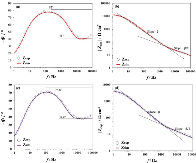
In contrast, the fitting of the experimental data works much better using Model 2 with CZnO << Cdl (Eq. (14)), as shown in Figure 8. Zexp was recorded at -0.4 V and -0.5 V. The
corresponding fitting parameters are listed in Table 2. Zexp is very well described by Zsim at all
frequencies. At low frequencies, the values of the phase (82° at -0.4 V and 76.8° at -0.5 V) correspond to the limiting phase of the CPE of Eq. (6) and are equal to β x 90°. At high frequencies, the phase values (41° at -0.4 V and 38.4° at -0.5 V) correspond to the half of the limiting phase of the CPE appearing in the square root function in Eq. (9). Similarly, the slope of the modulus Bode plot is -β at low frequencies (derived from Eq. 6) and -β/2 at high frequencies (derived from Eq. 9).
15
Figure 8: Fitting results for the columnar ZnO using Model 2 (with CZnO << Cdl). Re-corrected Bode plots obtained at -0.4 V: (a) phase and (b) modulus. Re-corrected Bode plots obtained at -0.5 V: (c) phase and (d) modulus. The open symbols represent the experimental data (Zexp) and the solid lines the simulated data (Zsim).
Table 2: Results of the fitting process for the columnar ZnO layers (Fig. 8) using Model 2 with CZnO << Cdl. E (V) Re (Ω cm2) Rct (Ω cm2) R0/n2 (Ω cm3) R1 (Ω cm) Qpore -1cm-2s β QZnO -1cm-2s CZnO (μF cm-2) -0.4 13.2 1.4 10+4 0.21 1.3 10+4 1.7 10-8 0.90 3.9 10-6 1.46 -0.5 13.8 4.5 10+3 0.23 8.3 10+3 7.7 10-8 0.85 1.46 10-5 3.3
16
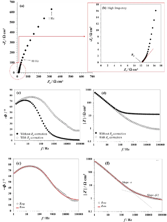
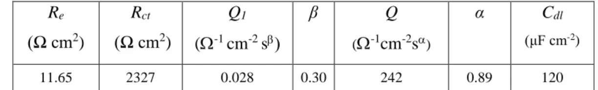
For comparison purpose, Figure 9 shows the experimental impedance of the nano-granular ZnO recorded at -0.7 V and the fitting curves using Model 2 with CZnO >> Cdl (Eq. (15)). This
potential was chosen since it was also selected to investigate oxygen reduction with similar films in a recent RRDE study [16].
Figure 9: Typical EIS diagrams for nano-granular ZnO (recorded at -0.7 V). (a) Nyquist plot with (b) zoom in high frequency to determine the electrolyte resistance (Re). Bode plots (without and with Re
17
correction): (c) phase curve and (d) modulus curve. Fitting results using Model 2 (with CZnO >> Cdl): (e) phase curve and (f) modulus curve. The open symbols represent the experimental data (Zexp) and the solid lines the simulated data (Zsim).
Zsim describes Zexp very well in the whole frequency range. The obtained fitting parameters are
listed in Table 3. The values of Cdl, that are close to their usual range of ca. 10-100 μF/cm2,
confirm that ZZnO is small due to its large capacitance. This is consistent with a penetration of
the electrolyte in a nanoporous layer exhibiting many small pores as those observed in the ex situ HAADF-STEM analysis (Figure 2b).
Table 3: Results of the fitting process for nano-granular ZnO (Fig. 9e and 9f) using Model 2 with CZnO >> Cdl. Re (Ω cm2) Rct (Ω cm2) Q1 (-1 cm-2 s β Q (-1cm-2s) α Cdl (μF cm-2) 11.65 2327 0.028 0.30 242 0.89 120
In the modulus plot (Figure 9f), the slope - in low frequency range corresponds to Zdl (Eq.
(4)) while the slope -/2 at high frequency relates to ZZnO (Eq. (9)). The value is low in
agreement with the small limiting phase obtained in high frequency (Figure 9e). This can be explained by a pore-in-pore model as described elsewhere in the literature [1, 38-40]. These results, along with those on columnar ZnO, demonstrate that EIS is a powerful tool to discriminate the scale of different defects (microscale cracks vs. nanoscale pores).
Model 2 (with CZnO << Cdl) was also successfully applied to the columnar ZnO at different
cathodic potentials between -0.3 V and -0.5 V (potentiostatic polarization). Furthermore, time-lapse EIS measurements were carried out to establish the dependence of CZnO on time.
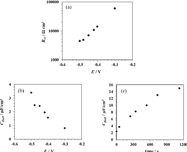
The resulting CZnO and Rct values are reported in Figure 10. Rct exhibits an exponential
dependence on the applied potential which can be explained by the oxygen reduction kinetics being essentially limited by charge transfer (Fig. 10a). Though it is not the main focus of the study, this result stands for the physical reliability of the model and the efficiency of the fitting process.
CZnO increases with increasingly negative potential (Fig. 10b) and with time (Fig. 10c). This is
consistent with a potential-dependant crack propagation since, in first approximation, CZnO is
18
the surfaces was carried out after polarization at -0.4 V and -0.5 V (Figure 11). There is no obvious sign of degradation on the ZnO surface after the polarization at -0.4V. In contrast, Figure 11b reveals significant damages after the polarization at -0.5 V. The propagation of the cracks goes from the surface towards the substrate till causing local delamination of the films. The propagation probably starts from the defects already present in the as-deposited state (Fig. 3a) and goes along the column boundaries.
Figure 10: Application of Model 2 (with CZnO << Cdl) to columnar ZnO films polarized at different potentials E: (a) Rct as a function of E; (b) CZnO as a function of E and (c) CZnO as a function of time obtained from time-lapse EIS at -0.5 V.
Crack propagation is already initiated between -0.3 V and -0.4 V which is much lower than the film rupture potential estimated at ca. -0.6 V by potentiodynamic voltammetry (Fig. 4). This is explained by the fact that, in this model, CZnO is “visible” (i.e. not masked by the double layer
capacitance Cdl) only when it has a low value, which corresponds to the first stages of
degradation. The latter can go unnoticed if investigated with solely ex situ SEM top-view imaging that show only the state of the surface and not the inner walls of the cracks. This proves
19
that EIS is a more sensitive technique than DC polarization curves and scanning electron microscopy to evidence the beginning of crack propagation towards the substrate.
The low values of CZnO also suggest that the formation of cracks is localized. EIS measurements
provide only global “averaged” information over the whole surface of the ZnO in contact with the electrolyte. The depth, the width and the spatial distribution of the cracks cannot be assessed. A zoom-out on the micrograph of the sample polarized at -0.5 V (Figure 11c) evidences that the delamination is localized in some areas (where the copper substrate is clearly visible) while other areas look damage-free. When this delamination state is reached, the model developed in this study, that characterizes the ZnO/electrolyte interface, becomes less reliable since the copper substrate is exposed to the electrolyte and part of the stress causing the degradation has vanished.
Figure 11: Post-mortem analysis of the columnar ZnO layers at different potentials. Top-view SEM micrographs after potentiostatic polarization at -0.4 V (a) and at -0.5 V (b,c). The copper substrate appears in darker contrast as the ZnO layer.
Since the film rupture clearly depends on the applied potential (Fig. 4 and Fig. 11), it can be postulated that the stress necessary to generate the cracks might originate from the piezoelectric properties of columnar ZnO [41-43]. The smooth dependence of CZnO on the applied potential
20
(Figure 10b) also hints at this hypothesis. However, in order to validate this assumption, more research work is needed, e.g. in the direction of stress measurements and modelling of thin textured oxide layers under mechanical stress [44,45]. Those activities are beyond the scope of the present study that aims at evidencing structural defects (and their propagation) in thin films using electrochemical methods.
Figure 12 schematically summarizes the main findings of this study on columnar ZnO. Three scenarios are considered based on different layer structures and on their apparent capacitance, C, “visible” by EIS. Results on nanoporous ZnO are also displayed for comparison.
Figure 12a shows a fully dense structure. The latter is in accordance with the STEM analysis (Figure 2a). For such structure, Model 1 (Figure 6a) is suitable and Cshould be in the range of usual double layer capacitance values, i.e. 10-100 µF/cm2. Yet the value of C observed during EIS experiments is much lower. Hence this scenario is rejected.
Figure 12b shows the same columnar layer as in Figure 12a but with numerous gaps between the columns. From the impedance viewpoint, this open nanostructure is close to that of the nano-granular ZnO (Figure 12d) and would yield a Cvalue around 10-100 µF/cm2 (Model 2, CZnO >> Cdl, Figure 12f). Virtually, this open nanostructure could have been generated by a
homogenous (i.e. non-localized) crack propagation along most of the column boundaries. This scenario is not supported by the post-mortem SEM analysis (showing localized degradation, Fig. 11c) and is therefore also invalid.
Thus, the only way to explain the low and increasing capacitance value of the columnar film during polarization is the localized crack propagation (leading to microscale damages and delamination) in an originally dense structure (at the nanoscale), as shown in Figure 12c. In terms of impedance modulus, this scenario leads to the case where CZnO << Cdl and therefore
21
Figure 12: Schematic interpretation of the influence of the structural defects of the ZnO layers (a-d) on the impedance response (e-f) using Model 2 where ZZnO and Zdl are in series (Figure 6b). The change of slope in
the ZZnO plots relates to different dependencies on the frequency (compare Eq. (6) and Eq (9)). When CZnO << Cdl, (e), ZZnO + Zdl ~ ZZnO and solely ZZnO is “visible” (measured). In contrast, when CZnO >> Cdl, (f), ZZnO + Zdl ~ Zdl at low frequencies (typically below 1000 Hz) and ZZnO + Zdl ~ ZZnO at high frequencies (typically
above 5000 Hz).
22
3. Conclusions
The degradation of columnar ZnO layers under cathodic polarization was investigated by EIS and electron microscopy. It was found that the structure of the as-deposited films was dense at the nanoscale with no gaps between the columns. An equivalent circuit model including a de Levie impedance was developed to account for the pores and cracks of the layers. The model took advantage of the flexibility of the de Levie impedance that can describe “real” electrodes whose microstructures are far from an ideal array of identical cylindrical pores developed in the initial theory. The propagation of cracks in the ZnO layers generates a capacitance (CZnO)
that is approximated to be proportional to the crack inner surface in contact with the electrolyte. Due to its localized nature, CZnO is sufficiently small so that its impedance is not masked by
that of the double layer capacitance existing at the top of the ZnO surface. This stands in contrast with homogeneously distributed defects, like those of a nanoscaled pore network, that yield large CZnO values. Therefore, in this case study on sputtered layers, EIS proved to be an
efficient tool to unambiguously distinguish structural defects of different scales (microscaled vs. nanoscaled) and to evidence the early stages of degradation of a conductive coating.
Acknowledgements
The financial support by the Association Nationale de la Recherche et de la Technologie (ANRT, Paris, France, contract CIFRE n° 2016/0066) is gratefully acknowledged. This work was also supported by the European Union through the European Regional Development Fund (ERDF), the Ministry of Higher Education and Research, the Région Bretagne, the Conseil Général du Finistère and Brest Métropole Océane, through the CPER Project 2015–2020 MATECOM. The authors thank Luiz F.G. Morales and Christian Zaubitzer (ScopeM, ETH Zurich) for technical support with HAADF-STEM experiments.
References
[1] M. E. Orazem, B. Tribollet, Electrochemical Impedance Spectroscopy, John Wiley & Sons, 2nd ed., 2017.
[2] T. Barres, B. Tribollet, O. Stephan, H. Montigaud, M. Boinet, Y. Cohin, Electrochim. Acta
2017, 227, 1.
23
[4] B. Hirschorn, M. Orazem, B. Tribollet, V. Vivier, I. Frateur, M. Musiani, J. Electrochem. Soc. 2010, 157, C452.
[5] R. de Levie, Electrochemical response of porous and rough electrodes, Adv. Electrochem. Eng. 1967, 6, 329.
[6] O. E. Barcia, E. D. Elia, I. Frateur, O. R. Mattos, N. Pébère, B. Tribollet, Electrochim. Acta
2002, 47, 2109.
[7] Lasia, J. Electroanal. Chem. 1995, 397, 27.
[8] C. Hitz, A. Lasia, J. Electroanal. Chem. 2001, 500, 213.
[9] J.-P. Candy, P. Fouilloux, M. Keddam, H. Takenouti, Electrochim. Acta 1982, 27, 1585. [10] W. Gao, Z. Li, Ceram. Internat. 2004, 30, 1155.
[11] M. A. Borysiewicz, E. Dynowska, V. Kolkovsky, M. Wielgus, K. Golaszewska, E. Kaminska, M. Ekielski, P. Struk, T. Pustelny, A. Piotrowska, Mater. Res. Soc. Symp. Proc.
2013, 1494, 71.
[12] Z. Onuk, N. Rujisamphan, R. Murray, M. Bah, M. Tomakin, S. I. Shah, Appl. Surf. Sci.
2017, 396, 1458.
[13] I. Sayago, M. Aleixandre, L. Arés, M. J. Fernández, J. P. Santos, J. Gutiérrez, M. C. Horrillo, Appl. Surf. Sci. 2005, 245, 273.
[14] M. Prestat, J. Soares Costa, B. Lescop, S. Rioual, L. Holzer, D. Thierry, ChemElectroChem 2018, 5, 1203.
[15] M. Prestat, L. Holzer, B. Lescop, S. Rioual, C. Zaubitzer, E. Diler, D. Thierry, Electrochem. Commun. 2017, 81, 56.
[16] J. Soares Costa, M. Prestat, B. Lescop, S. Rioual, B. Tribollet, L. Holzer, K. Pélissier, D. Thierry, ChemElectroChem 2019, 6, 5321.
[17] S. Thomas, I.S. Cole, N. Birbilis, J. Electrochem. Soc. 2013, 160, C59.
[18] S. Thomas, I.S. Cole, M. Sridhar, N. Birbilis, Electrochim. Acta 2013, 97, 192. [19] S. Thomas, N. Birbilis, M.S. Venkatraman, I.S. Cole, Corros. Sci. 2013, 69, 11. [20] M.S. Venkatraman, I.S. Cole, B. Emmanuel, Electrochim. Acta 2011, 56, 8192.
[21] M. Prestat, F. Vucko, B. Lescop, S. Rioual, F. Peltier, D. Thierry, Electrochim. Acta 2016, 218, 228.
[22] T. Prosek, A. Nazarov, U. Bexell, D. Thierry, J. Serak, Corros. Sci. 2008, 50, 2216. [23] J. Stoulil, T. Prosek, A. Nazarov, J. Oswald, P. Kriz, D. Thierry, Mater. Corros. 2015, 66, 777.
[24] I. S. Cole, Materials 2017, 10, 1288.
24
[26] S. S. Lin, J. L. Huang, Surf. Coat. Tech. 2004, 185, 222.
[27] J. Hüpkes, J. I. Owen, S. E. Pust, E. Bunte, ChemPhysChem 2012, 13, 66. [28] J. Han, W. Qiu, W. Gao, J. Hazard. Mater. 2010, 178, 115.
[29] Z. Onuk, N. Rujisamphan, R. Murray, M. Bah, M. Tomakin, S. I. Shah, Appl. Surf. Sci.
2017, 396, 1458.
[30] J. Sakabe, N. Ohta, T. Ohnishi, K. Mitsuishi, K. Takada, Commun. Chem. 2018, 1, art. #24.
[31] V. Godinho, P. Moskovkin, R. Álvarez, J. Caballero-Hernández, R. Schierholz, B. Bera, J. Demarche, A. Palmero, A. Fernández, S. Lucas, Nanotechnology 2014, 25, art. #355705. [32] H. S. Wroblowa, S. B. Qaderi, J. Electroanal. Chem. 1990, 153, 295.
[33] N. Heller-Ling, M. Prestat, J. L. Gautier, J. F. Koenig, G. Poillerat, P. Chartier, Electrochim. Acta 1997, 42, 197.
[34] T. T. M Tran, B. Tribollet, E. M. M Sutter, Electrochim. Acta 2016, 216, 58.
[35] B. Hirschorn, M.E. Orazem, B. Tribollet, V. Vivier, I. Frateur, M. Musiani, J. Electrochem. Soc. 2010, 157, C458.
[36] M. E. Orazem, N. Pébère, B. Tribollet, J. Electrochem. Soc. 2006, 153, B129.
[37] G. J. Brug, A. L. G. Van Den Eeden, M. Sluyters-Rehbach, J. H. Sluyters, J. Electroanal. Chem. 1984, 176, 275.
[38] M. Itagaki, Y. Hatada, I. Shitanda, and K. Watanabe, Electrochim. Acta 2010, 55, 6255. [39] Y. Gourbeyre, B. Tribollet, C. Dagbert, and L. Hyspecka, J. Electrochem. Soc. 2006, 153, B162.
[40] Y. Ben Amor, E. Sutter, H. Takenouti, M. E. Orazem, B. Tribollet, J. Electrochem. Soc.
2014, 161, C573.
[41] S.Y. Chu, W. Water, J.T. Liaw, J. Eur. Ceram. Soc. 2003, 23, 1593. [42] K. B. Sundaram, A. Khan, Thin Solid Films 1997, 295, 87.
[43] Y. H. Hsu, J. Lin, W. C. Tang, J. Mater. Sci.: Mater. Electron. 2008, 19, 653. [44] Y. Safa, T. Hocker, M. Prestat, A. Evans, J. Power Sources 2014, 250, 332.
[45] A. Evans, M. Prestat, R. Tölke, M.V.F. Schlupp, L.J. Gauckler, Y. Safa, T. Hocker, J. Courbat, D. Briand, N.F. de Rooij, D. Courty, Fuel Cells 2012, 12, 614.