Faculte de genie
Departement de genie electrique et de genie informatique
CHARACTERIZATION OF AMORPHOUS SILICON
CARBIDE AND ITS APPLICATION TO CONTACT BARRIER
DIODE
CARACTERISATION DE CARBURE DE SILICIUM
AMORPHE ET SON APPLICATION A LA DIODE A
BARRIERE DE CONTACT
These de doctorat (Ph.D) Speciality: genie electrique
Professeur Cetin Aktik Professeur Mihai Scarlete Professeur Rejean Fontaine Dr. Abdossamad Talebpour
TAHEREH FANAEISHEIKHOLESLAMI
Published Heritage Branch 395 Wellington Street Ottawa ON K1A0N4 Canada Direction du Patrimoine de I'edition 395, rue Wellington Ottawa ON K1A0N4 Canada
Your file Votre reference ISBN: 978-0-494-48550-7 Our file Notre reference ISBN: 978-0-494-48550-7
NOTICE:
The author has granted a non-exclusive license allowing Library and Archives Canada to reproduce, publish, archive, preserve, conserve, communicate to the public by
telecommunication or on the Internet, loan, distribute and sell theses
worldwide, for commercial or non-commercial purposes, in microform, paper, electronic and/or any other formats.
AVIS:
L'auteur a accorde une licence non exclusive permettant a la Bibliotheque et Archives Canada de reproduire, publier, archiver,
sauvegarder, conserver, transmettre au public par telecommunication ou par Plntemet, prefer, distribuer et vendre des theses partout dans le monde, a des fins commerciales ou autres, sur support microforme, papier, electronique et/ou autres formats.
The author retains copyright ownership and moral rights in this thesis. Neither the thesis nor substantial extracts from it may be printed or otherwise reproduced without the author's permission.
L'auteur conserve la propriete du droit d'auteur et des droits moraux qui protege cette these. Ni la these ni des extraits substantiels de celle-ci ne doivent etre imprimes ou autrement reproduits sans son autorisation.
In compliance with the Canadian Privacy Act some supporting forms may have been removed from this thesis.
Conformement a la loi canadienne sur la protection de la vie privee, quelques formulaires secondaires ont ete enleves de cette these.
While these forms may be included in the document page count,
their removal does not represent any loss of content from the thesis.
Bien que ces formulaires
aient inclus dans la pagination, il n'y aura aucun contenu manquant.
Des couches minces du carbure silicium amorphe ont ete preparees en utilisant un procede de deposition en phase vapeur ayant comme source des polymeres (PS-CVD). Les couches ont ete deposees a des temperatures qui varient entre 750 et 1000 °C. Les substrats utilises pour les depots sont en silicium cristallin du type p et n, et en dioxyde de silicium (SiOa) obtenu par croissance thermique. Les proprietes chimiques et electriques des couches ont ete etudiees par diverses techniques, y compris la spectroscopic infrarouge par transformde de Fourier, detection de recul elastique (ERD), et la mesure de capacite-tension. Nous avons observe une correlation entre la concentration moyenne de l'oxygene dans les films et la temperature de deposition, liant une faible concentration en oxygene dans le film a une temperature elevee de deposition. Cependant, la concentration de l'oxygene dans les films deposes a la meme temperature etait independante du substrat. Les couches minces deposees a basse temperature ont demontre un comportement isolant, alors qu'un comportement semi-conducteur est obtenu a temperature elevee. Des contacts ohmiques ont ete obtenus sur la couche mince de carbure de silicium amorphe (a-SiC) en evaporant des contacts de nickel, suivis d'un recuit a 800 °C pendant 2 minutes. La mobilite de Hall moyenne obtenue est d'environ 34 cm2/V.s pour les echantillons deposes sur SiCh a 1000 °C.
Les caractdristiques generates du a-SiC depose a 750 °C, ont ete etudiees se servant des heterostructures de SiC/c-Si utilisees comme des diodes a barriere de contact. Les proprietes de transport du courant dans la couche mince de a-SiC deposee sur un substrat de c-Si de type-p ont ete etudiees en utilisant des mesures courant-tension (IV) et capacite-tension (CV). Les caracteristiques IV ont montre qu'une dependance exponentielle du courant aux tensions est applicable pour les basses tensions tandis que la caracteristique de courant limite par les charges de l'espace est dominante pour les hautes tensions. Les caracteristiques de CV ont indique un comportement de type-p pour a-SiC resultant de la charge positive injectee par le substrat de silicium. La mobilite des trous et la duree de vie des porteurs injectes dans la couche mince de a-SiC ont ete calculees en utilisant un modele du courant limite par les charges d'espace. La variation de la mobilite effective des trous de a-SiC varie entre 10"4 et
Thin films of amorphous silicon carbide were prepared using Polymer-Source Chemical Vapor Deposition (PS-CVD) at temperatures between 750 and 1000 °C. The substrates were silicon single crystal wafers of p-type and n-type, and thermally-grown silicon dioxide substrates. The chemical and electrical properties of the films were studied by various techniques, including Fourier-transform infrared spectroscopy, Elastic Recoil Detection (ERD), and capacitance-voltage technique. A correlation was observed between the average concentration of oxygen in the films and the deposition temperature, linking a low oxygen concentration in the film to a high deposition temperature. However, the concentration of oxygen in the films deposited at the same temperature was independent of the substrate. The thin films deposited at low temperature showed insulating behaviour, while the semiconducting behaviour was obtained at high deposition temperatures. Ohmic contacts were obtained on the deposited a-SiC thin film by evaporating nickel contacts, followed by annealing of the sample at 800 °C for 2 minutes. The average Hall mobility was found about UH = 34 cm2/V.s for the samples deposited on SiC^ substrate at 1000 °C.
The general characteristics of wide band gap SiC deposited at 750 °C, was studied using a-SiC/c-Si heterostructures applied as the contact barrier diodes. The current transport properties of a-SiC thin film deposited on a p-type silicon c-Si substrate were investigated using current-voltage (IV) and capacitance-voltage (CV) measurements. IV characteristics showed an exponential dependence of current to the applied voltages for low forward bias while the space charge limited current characteristics dominated for higher forward bias. CV characteristics indicated a p-type property for a-SiC which is resulted by the injected positive charge from p-type silicon substrate. The hole mobility and injected carrier lifetime in a-SiC thin film was calculated using a model of space-charge limited current. The variation in effective hole mobility of a-SiC, which was ranged between 10"4 and 10"7, was attributed to
Je tiens a exprimer ma plus profonde reconnaissance a mon directeur et co-directeur de these, le professeur Qetin Aktik et le professeur Mihai Scarlete, pour leurs conseils precieux et eclaires.
Je voudrais remercier les membres du Jury d'avoir accepte d'examiner ce travail.
Je voudrai aussi remercier tous ceux et celles qui ont contribue, de pres ou de loin a l'aboutissement de ce travail. Je voudrais remercier les membres de la compagnie Sixtron en particulier Mme. Nathalie Camire pour la preparation des echantillons. Je voudrais remercier tous les techniciens de salle blanche pour leur aide pendant la caract6risation des echantillons. Je voudrais remercier Dr. Subhash Gujrathi pour sa contribution dans la caracterisation chimique. Je voudrais remercier tous mes colleges en particulier M. El Hassane Oulachgar pour les discussions techniques.
Enfin, je voudrai exprimer ma reconnaissance a mon mari, professeur Amin Behzadmehr pour son grand support technique et moral tout au long de mes etudes, et ma grande famille en Iran pour le grand appui moral qu'elle a su m'apporter.
CHAPTER 1: INTRODUCTION 1 CHAPTER 2: BIBLIOGRAPHY 5
2.2. EFFECT OF DEPOSITION CONDITIONS 8 2.3. TRANSPORT PROPERTIES OF A-SIC 10 2.4. A-SIC/C-SIHETEROJUNCTION 11 2.5. APPLICATIONS OF A-SIC 14 2.5.1. OPTOELECTRONIC DEVICES 14 2.5.2. PASSIVATION LAYERS 16 2.5.3. COATING MATERIAL 17
CHAPTER 3: AMORPHOUS MATERIALS 19
3.1. MOBILITY OF CHARGE CARRIERS IN AMORPHOUS MATERIALS 20 3.2. APPLICATION OF AMORPHOUS MATERIALS IN CONTACT BARRIER DIODE 22
3.2.1. ROLE OF THE AMORPHOUS INTERLAYER 23 3.2.2. CAPACITANCE-VOLTAGE CHARACTERISTICS 23 3.2.3. CURRENT-VOLTAGE CHARACTERISTICS 25
CHAPTER 4: EXPERIMENTAL DETAILS 31
4.1. PREPARATION OF A-SIC 31 4.2. CHARACTERIZATION METHODS 32
4.2.1. ERD MEASUREMENTS 33 4.2.2. HALL MEASUREMENTS 33
CHAPTER 5: MATERIAL CHARACTERIZATION AND DISCUSSION 37
5.1. MATERIAL CHARACTERIZATION 37 5.2. CONTACT CHARACTERIZATION 47 5.3. RESULTS OF MOBILITY MEASUREMENTS 49
CHAPTER 6: APPLICATION OF ASIC LAYERS IN CONTACT BARRIER
DIODES 51
6.1. IV CHARACTERISTICS 54 6.2. CV CHARACTERISTICS 58 6.3. MOBILITY AND LIFETIME CALCULATION 62
Figure 2-1 An example of IR spectrum of a-SiC films
Figure 2-2 Various possible configurations of CH3 groups attached to silicon in a-Sii.xCx:H
films. Note that Y is either Si or C, not attached to three hydrogen atomes
Figure 2-3 The absorption strength of the main IR absorption bands as a function of carbon-content (x). Note that the two Si-H curves and the Si-C and Si-CH3 curves are based on the deconvolution of the corresponding absorption peaks into Gaussian subpeaks
Figure 3-1 Models illustrating the structure of (a) crystalline and (b) amorphous materials
Figure 3-2 Room temperature capacitance voltage characteristics of undoped a-Si:H/p-c-Si (NA = 1016 cm'3) heteroj unction
Figure 3-3 Current-voltage characteristics of undoped a-Si:H/p-c-Si (NA = 10 cm ) heterojunction
Figure 4-1 The arbitrary shaped samples for Hall measurements: (a) and (b) acceptable to determine the carrier concentration, carrier type, resistivity, and mobility, (c) recommended only for mobility measurement
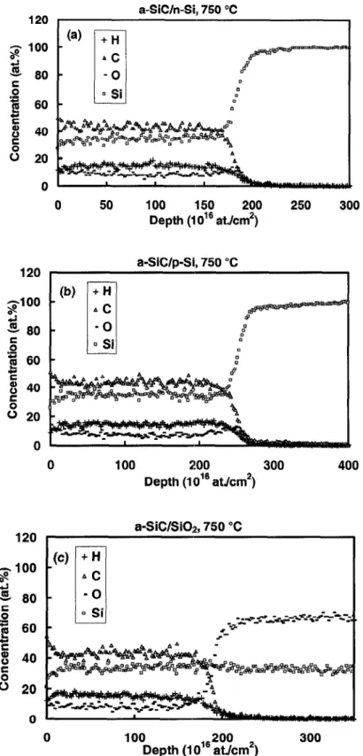
Figure 5-1 FT-IR spectra in the 500-1500 cm"1 region of thin film deposited at temperatures
of 750, 850, 950 and 1000 °C on (a) n-type silicon substrate, (b) p-type silicon substrate, and (c) silicon dioxide thermally grown on silicon substrate
Figure 5-2 ERD measurement of thin film deposited at 750 °C on (a) n-type silicon substrate, (b) p-type silicon substrate, and (c) silicon dioxide thermally grown on silicon substrate
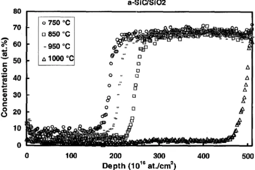
1000 °C on Si0 substrate
Figure 5-4 Oxygen concentration in the films deposited at temperatures of 750, 850, 950 and 1000 °C on Si02 substrate
Figure 5-5 CV curve of thin film deposited at 750 °C, 850 °C, and 950 °C on n-type silicon substrate
Figure 5-6 CV curve of thin film deposited at 750 °C, 850 °C, and 950 °C on p-type silicon substrate
Figure 5-7 CV curve of thin film deposited at 750 °C, 850 °C, and 950 °C on silicon dioxide substrate
Figure 5-8 CV curve of thin film deposited at 1000 °C, (a) on n-type silicon, (b) on p-type silicon, (c) on silicon dioxide
Figure 5-9 Current-voltage characteristic of nickel contact of deposited thin film at 1000 °C (a) before annealing, (b) after annealing
Figure 5-10 ERD measurement of thin film deposited at 1000 °C on Si02 substrate
Figure 6-1 ERD depth profiles of elements in Ni/SiC/p-Si/Al diodes for the thickness of a-SiC layer; a) 215 nm, b) 270 nm, and c) 270 nm
Figure 6-2 IV characteristic for the three Ni/a-SiC/p-Si samples. Two samples have 270 nm a-SiC, and one other has 215 nm a-SiC
Figure 6-4 Forward current characteristic on a log-log scale of the Ni/a-SiC/p-Si devices
Figure 6-5 CV characteristic for the three Ni/a-SiC/p-Si samples. Two samples have 270 nm a-SiC, and one other has 215 nm a-SiC
Figure 6-6 A /C vs. voltage for the Ni/a-SiC/p-Si heterostructures
Figure 6-7 Equivalent circuit of contact barrier diode
Figure 6-8 Effective mobility of a-SiC Qieff) vs. applied voltage (Va) for higher forward
biased Ni/a-SiC/p-Si contact barrier diodes
Figure 6-9 Effective mobility of a-SiC (/teg) vs. applied voltage (Va) for higher lower biased
Ni/a-SiC/p-Si contact barrier diodes
Figure 6-10 Voltage drop across the organic layer (Vsc) vs. applied voltage (Va) for
Ni/a-SiC/p-Si devices
Figure 6-11 Lifetime of injected carriers (T) VS. applied voltage (Va) for higher forward biased
Ni/a-SiC/p-Si contact barrier diodes
Figure 6-12 Lifetime of injected carriers (r) vs. applied voltage (Va) for lower forward biased
Ni/a-SiC/p-Si contact barrier diodes
Figure 6-13 Electric field in the space-charge layer (Esc) and in the substrate (Esi) of
TABLE 4-1 DEPOSITION CONDITIONS FOR A-SIC THIN FILMS
TABLE 6-1 ELECTRICAL PROPERTIES OF NI/A-SIC/P-SI CONTACT BARRIER DIODES OBTAINED FROM IV ANALYSIS
TABLE 6-2 ELECTRICAL PROPERTIES OF NI/A-SIC/P-SI CONTACT BARRIER DIODES OBTAINED FROM CV ANALYSIS
CHAPTER 1: INTRODUCTION
The thin films are the key elements for continued technological advances in the fields of electronic, photonic, and magnetic devices. The synthesis of materials as thin films enables easy integration of various types of devices. The thin film modules are expected to be cheaper to manufacture owing to their reduced material, energy, handling and capital costs. The introduction of large area thin film amorphous semiconductors with low cost fabrication capability has not only given a new impetus to the field of optoelectronic devices, such as solar cells, flat panel displays, image sensors or printer heads, but it now also forms the basis for large area of microelectronic devices. The amorphous semiconductors lack long rang ordering of their constituent atoms, but they do have local order on the atomic scale. This short range order is directly responsible for observable semiconductor properties such as optical absorption edges and activated electrical conductivities. The discovery of the ability to control the optical band gap energies by alloying silicon with other elements has introduced a new phase in the field of amorphous semiconductors.
One of the promising materials for various applications in opto- and micro-electronic devices is the thin film amorphous silicon carbide (a-SiC). This thermally and chemically stable wide band gap material has superior mechanical strength, high radiation resistance and high optical transmittance [NELSON et al., 1966, DEMISHELIS et al., 1991, El KHAKANI et al., 1993]. The preparation methods and the deposition conditions have a significant effect on electrical properties of a-SiC such as conductivity and transport prosperities. For example, thin films of a-SiC with the band gap larger than 1.9 eV require the inclusion of larger amounts of carbon. The increasing of carbon content in the film leads to a higher increased midgap state density and limits the transport properties of the undoped a-SiC. Moreover, it is difficult to add impurity as doping to the wide band gap a-SiC due to the high localized tail density of states associated with both band edges and midgap state density [KANICKI, 1991].
Recently, SiC has been prepared using different deposition or growing methods. Chemical vapour deposition (CVD) is a widely used technique for the preparation of crystalline and
polycrystalline silicon carbide. Very high temperatures (1400-2200 °C) are needed for the preparation of crystalline SiC from gas mixtures that contain molecules such as SiCU, CH4, H2, or H3C+SiCl3 [SCHLICHTING, 1980]. Microcrystalline SiC can be obtained at
temperatures below 1200 °C [O'CONNOR et al., I960]. The possibility of preparing a-SiC films by CVD method using simple molecules such as SiCU and CH4 was studied by Bullot et Schmit [BULLOT et al., 1987]. but only the simple molecule such as CH4, SiHCl3, SiCU,
and HC1 were detected in presence of hydrogen. Thus, it was concluded that this method is not suitable for preparing a-SiC films. The decomposition reactions of several more complicated organosilicon compounds for the deposition of a-SiC films has been reported
[GERAULT et al., 1982, GERAULT et al, 1983, GERAULT et al., 1984]. The films prepared by the decomposition of these organosilicon compounds contained between 24 and 82 percent silicon, depending on the source gas and the substrate temperature. Plasma-enhanced chemical vapor deposition (PECVD) has become the most commonly used method in the a-SiC film deposition. It was found that the structure of the a-SiC thin films grown on Si-substrates depends strongly upon the deposition condition such as source, substrate temperature, pressure, etc. [CHO et al., 2002]. The majority of deposition systems currently used are capacitively coupled and the gas mixture is S1H4 + CH4. The substrate temperature is mostly in the range of 200 to 300 °C, and the pressure is 0.1 to 1 Torr. There are wide variations in the power used in these systems [CHOI, 2001, CHO et al., 2006, TAKAHASHI et al., 1997, EICKHOFF et al., 2004]. This method is associated with high preparation costs, involves relatively expensive equipment, and is a time-consuming procedure [SHIOZAWA et al., 1995]. Because of the interesting properties of the a-SiC thin film, the economic interest in the production of this material is high and needs to look for a lower cost method. Alternatively, polymeric precursors have been used to synthesize silicon carbide [KHO et a., 2001, RAMAKRISHNAN et al., 2001, DISMUKES et al., 1997]. Further, in a relatively recent development [SCARLETE et al., 2003], polysilane precursors have been used in the Polymer-Source Chemical Vapor Deposition (PS-CVD) method to synthesize thin films of a-SiC. The most significant advantage of the PS-CVD method is the high deposition rate resulting from a) the in situ synthesis in the reactor of the gaseous ceramic precursors with the highest known density to date (around 300 a.m.u.), and b) the involvement of a specific fast mechanism of synchronized SiC bonds rearrangement [SCARLETE et al., 1994,
SCARLETE et al., 1995]. Additional advantages of the PS-CVD method are the simplicity of the equipments and handling procedures due to the deposition at atmospheric pressure, which eliminates the requirements for expensive equipment imposed by classic CVD methods. In addition, the operation involves a reasonably stable precursor and reduced health hazard [SCARLETE etal., 2003].
DC conductivity of a-SiC films consists of hopping conduction in the conduction band tail plus tunnelling from localized states to the dangling bond defects [BULLOT et al., 1987]. The activation energy for the extended state conduction (AEi) is defined as AEi= EC-EF,
where Ec is the conduction band edge and EF is the Fermi energy level. The activation energy
for the hopping conduction (AE2) can then be expressed as AE2= EA-EF+W [MOT et al.,
1979], where EA is the conduction band tail edge and W is the hopping activation energy of electrons in the band tail. Therefore, the band tail width increases upon carbon incorporation, which means that carbon incorporation increases disorder in these alloys [RIZK et al., 1987]. The undoped samples of a-SiC exhibit a single activation energy that is consistent with conduction via the extended states [DEMICHELIS et al., 1991]. The conductivity of doped samples at high temperatures corresponds to the extended states but near the room temperature the transport mechanism occurs by phonon-assisted hopping. The electrical properties of a-SiC could be investigated using a-SiC/c-Si heterostructures [MEGAFAS et al., 1992, MARSAL et al., 1997, MARSAL et al., 1999, CHOI et al., 2000]. This heterostructure shows the rectifying property over a large voltage range. The characterization results are used to explore some electrical properties of a-SiC such as dielectric constant, impurity concentration, electron affinity, breakdown voltage, mobility, and lifetime. The electron and hole mobility of a-SiC have been already measured using Hall measurements [NEBEL et al., 1993], time-of-flight technique [BAYLAY et al., 1993, GU et al., 1994] and photomixing technique [TANG et al., 1995]. The electron mobility of a-SiC was reported to be between 1 to 10 c n ^ v V1 and the hole mobility ranged from lxlO"4 to 3x10 3 c m V ' s '1.
The aim of this work is to characterize a-SiC as a wide band gap material, in order to investigate the performance of contact barrier microelectronic devices. The a-SiC thin films have been prepared by PSCVD method. The major electrical characterization techniques
used in this work were IV and CV measurements. The transport properties of undoped a-SiC were studied directly by the Hall measurement technique and indirectly by using a heterostructure device. The characterization results were used to analyze the properties of the contact of a-SiC/c-Si, such as the ideality factor and barrier height. An immediate objective was to investigate some properties of the amorphous layer itself, such as dielectric constant, injected carrier lifetime and mobility.
This thesis will be presented the electronic properties of intrinsic a-SiC, and the potential application of this material in contact barrier devices. Chapter 2 is a review of the recent researches on the electrical properties and device application of a-SiC material. The theoretical aspects of amorphous materials, properties and characterization methods are presented in the chapter 3. In chapter 4, the experimental methods used in this work for preparation and characterization of a-SiC thin film are explained. The results of material characterization and application in the contact barrier devices together with the calculation results are presented and discussed in chapters 5 and 6. Finally, a conclusion section summarizes the important points provided in this work.
CHAPTER 2: BIBLIOGRAPHY
The optical and electrical properties of amorphous silicon-carbon (a-SiC) alloys were reported for the first time in 1968 by three groups [MAGOB et al., 1968, HERMAN et al., 1968, WEINREICH et al., 1968]. Since then, intense research has been carried out on a-SiC films because of its potential applications in electronics and optical devices. The first review on the physics of a-SiC was published by Bullot and Schmit [BULLOT et al., 1987], based on data published between 1968 and 1987. Another review on a-SiC film developments was presented by Choi [CHOI, 2001], based on publications which have been reported between
1987 and 2000.
A survey of papers on a-SiC films published over the last 30 years shows that the majority of such films were prepared by the PECVD method, using a mixture of silane and methane (SiKt+CH*) gases, with or without hydrogen (H2) dilution. The second most common deposition technique is sputtering. The unhydrogenated films are usually prepared by sputtering a polysilicon SiC target using argon (Ar). a-SiC films can be obtained by sputtering a crystalline silicon (c-Si) target in a CELH-Ar atmosphere, or by sputtering a polycrystalline SiC target in an Ar+H2 atmosphere. Two other preparation techniques for a-SiC are electron cyclotron resonance chemical vapour deposition (ECR-CVD) and photoinduced chemical vapor deposition.
Structural properties of a-SiC were studied by many researchers. The structural analysis methods which were frequently employed for the characterization of a-SiC films were the FT-IR, Raman, X-ray photoelectron, and Auger electron spectroscopy [WEIDER et al., 1987, CROS et al., 1992]. A detailed analysis of IR results obtained on a-SiC is presented in section 2.1. The effect of deposition conditions, as an important domain in a-SiC material, is a subject considered in section 2.2. A brief review on the transport properties of a-SiC is presented in section 2.3. The studies in transport properties of a-SiC using the junction of this material with crystalline semiconductors in terms of heterojunction are discussed in section 2.4. In the last section, some of the recent applications of a-SiC in optical and electrical devices will be presented.
2.1. IR spectroscopy of a-SiC
One of the commonly used techniques in the structural characterization of amorphous silicon carbide films is the Infrared spectroscopy [CHOI, 2001]. Figure 2-1 shows an IR spectrum of a-SiC films with characteristic peaks.
I
3s
irb i - U > Drbanc ? CO X3 < C-Hn Si—HA
..i,. J - , _, Si-CA
I \
1 \
Si-CH2| \K/ \
Si-CH3/ \ 1 i i. 3000 2500 2000 1500 Wavenumber (cm-1) 1000 500Figure 2-1 An example of IR spectrum of a-SiC films [MASTELARO et al., 1997]
The Si-C bond is partly ionic, and, therefore, IR absorption bands are expected for SiC vibrations. The broad peak between 700 and 800 cm"1 can be attributed to the Si-CH3 rocking
and to Si-C stretching mode. The peak at 900-1100 cm^corresponds to the C-Hn wagging
mode. The peak at 1250 cm"1 corresponds to the Si-CH3 bend. The peak at 2100 cm"1 is due
to the Si-Hx stretching modes. The C-Hn stretching modes are at identified around 2900 cm"1.
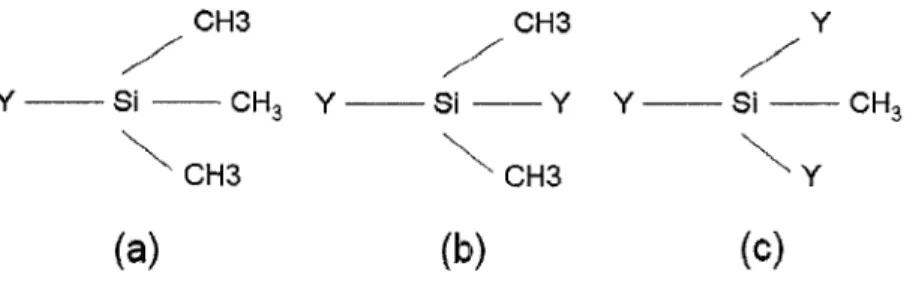
Wieder et al. [WIEDER et al., 1979] estimated the composition dependence of the absorption strength of the Si-C bonds from a simple effective charge model. The possible configurations of how the CH3 groups are attached to silicon are shown in figure 2-2 [WIEDER et al.,
1979]. Bullot and Schmidt indicated that mixing rocking or wagging vibrations with the Si-C stretching mode enhances the absorption strength because the C3 symmetry of methyl groups
important for the Si-CH3 rocking mode, because without this, it will not be mixed with the stretching mode. The CH3 wagging mode has rocking mode only in configuration (c) of figure 2-2, but it could be mixed in configurations (a) and (b).
,CH3 CH3 Y
Y Si CH3 Y Si Y Y Si CH3
x CH3 x CH3 x Y
(a) (b) (c)
Figure 2-2 Various possible configurations of CH3 groups attached to silicon in a-Sii_xCx:H
films. Note that Y is either Si or C not attached to three hydrogen atomes [WBEDER et al., 1979]
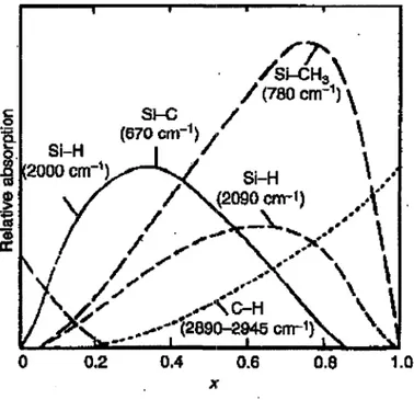
Mode coupling is responsible for the shift of the wagging band and the Si-C stretching band with film composition. Figure 2-3 plots the composition dependence of the integrated absorption strength of the main IR absorption bands [WIEDER et al., 1979]. It could be seen from this figure that the Si-C and Si-CH3 rocking and wagging modes at 670 and 780 cm"1
have different maxima as a function of x. The 780 cm'1 band appears only at carbon content
over 10%. At the low carbon content the carbon atoms are incorporated into the silicon network and are mostly bonded to silicon. The absence of C-H absorption bands in the low carbon content range may be due to the weak absorption coefficient of the C-H bonds. According to Wieder et al. [WIEDER et al., 1979], at the low carbon content of a-Si^C^H, the total hydrogen content increases between x=0 and x=0.3 because at this range, carbon atoms that are incorporated into the silicon network are always hydrogenated (CH or CH2).
f
I
Si-H 1(2000 cm-1) Si-C / (670 cm-1) / S J - C H3\ / (780 cm-1) \h
V ..--'.'(2890-2945 i 0.4 0.6 xFigure 2-3 The absorption intensity of the main IR absorption bands as a function of carbon-content (x). Note that the two Si-H curves and the Si-C and Si-CH3 curves are based on the deconvolution of the corresponding absorption peaks into Gaussian subpeaks [WIEDER et al., 1979]
2.2. Effect of deposition conditions
It is known that deposition conditions have significant effects on structural, electrical and optical properties of a-SiC. The recent studies on the deposition of a-SiC films using PECVD method include [MAHAN et al, 1985, MATSUDA et al., 1986, FOLSCH et al., 1992, LIN et al. 1987, SCFflFF et al., 1993]: The thin films of a-SiC with the band gap larger than 1.9 eV required the inclusion of larger amounts of carbon. However, as the band gap increases beyond 2 eV, the optoelectronic properties degrade and the Urbach energy and the sub band gap density of states or defects increase. This precluded the use of such materials in solar cells, tandem junction configuration or light emitting devices since the extra defects within the material act as efficient recombination centers. The addition of H2 to SiFu + CH4 plasma led to better optoelectronic properties, due to the increased energy gap, while the Urbach energy decreases results in increasing of the photoconductive gain. If the baseline material,
which has been deposited without hydrogen dilution, already shown good optoelectronic properties, the hydrogen dilution could be quite inefficient. Deichelis et al. [DEICHELIS et al., 1995] presented a method for establishing the optimum deposition conditions for a pure S1H4 + CH4 plasma in order to obtain a good quality baseline a-SiC:H material, by using an analytical method. They studied the effects of the CH4 flow, substrate temperature and the pressure on the optoelectronic properties of deposited films. They found that the optimized conditions were achieved at 20 seem CH4 flow, 325 °C substrate temperature, and the pressure in the range 0.4-1 Torr. Under these conditions, they obtained optimized films of a-SiC:H with energy gap in the rage of 1.84-1.9 eV, Urbach energies below 60 meV, and photoconductive gain higher than 106 cm2V"\
The effects of the deposition conditions on the transport properties of a-SiC has been studied by various research groups [KLAZES et al., 1982, LI et al., 1993, LI et al., 1992, LU et al., 1993]. Tang and Braunstein [TANG et al., 1995] determined the electron drift mobility, lifetime, and the conduction band Urbach energy of the if glow discharge of prepared a-SiC films, as a function of hydrogen dilution ratio (Hb/CCHi+SiFLO. They indicated that by increasing the hydrogen dilution ratio from 0 to 25, the band gap energy decrease from 1.94 to 1.9 eV, the electron drift mobility and lifetime increase from 4 to 7 cm2/Vs and 25 to 100
ns, respectively, and the Urbach Energy decrease from 47 to 43 meV. They concluded that for a-SiC:H films with increased hydrogen dilution ratio, the density of positively charged defects, negatively charged defects, and neutral defects all show a tendency to decrease.
Jung et al. [JUNG et al., 2003] deposited a-SiC on c-Si substrate by RF PECVD and by the thermal metal organic chemical vapor deposition (MOCVD) methods using a SiFLi + CH4 gas mixture and a single molecular precursor of diethylmethylsilane, respectively. They studied the effect of deposition parameters, such as deposition temperature, pressure, RF power, and annealing temperature on the structural and optical properties of a-SiC thin films. They realized that there were large variations in hydrogen contents and crystallinity in the films depending on the deposition and annealing temperatures. They indicated that the composition of films is changed from amorphous to polycrystalline and crystalline by increasing the deposition temperature from 700 to 1000 °C while the hydrogen content was decreased. It
was indicated that RF power is a main parameter for which the optical band gap is influenced rather than the annealing temperature. By increasing the RF power, the optical band gap energy increased from 3.68 to 4.09 eV, while the annealing temperature had no effect on the band gap energy. The FTIR result showed that the microcrystalline phase in the films was rapidly enhanced as the annealing temperature increased.
Like other properties, the dielectric constant of a-SiC can be affected by the deposition conditions. a-SiC is a potentially attractive low-k material due to its high electrical resistivity and its good thermal stability, both resulting from its highly cross-linked structure [ENDO et al., 1996, UOKOMICHI et al., 1998, CHO et al., 2000]. To reach lower k values, larger and more complex precursors, perhaps with cyclic molecular structure and more complex organic content, may be used to form cyclic structures with large open spaces inside the film. Li et al. [LI et al., 2003] used the PECVD technique with sources gases CH4, SiH4 and H2 at room
temperature and determined the deposition conditions that can lead to a-SiC films with lower dielectric constants. The dielectric constants were calculated from the high frequency (1 MHz) capacitance, measured on a metal-insulator-semiconductor structure formed with Au dot electrodes deposited on top of a-SiC by e-beam evaporation. The dielectric constants of the as-deposited films were found to vary with the RF power and CH4 gas flow ratio. The lowest dielectric constant obtained was 2.71, for films deposited at RF power of 70 W and flow rate of 30:50:50 seem for CH4:SiH4:H2, respectively. They determined the mass density from X-ray reflectivity measurements to be about 1.353 g cm"3. This value is smaller than the
mass densities of SiC«2 and SiC. They mentioned that the prepared film had nearly 77% C atom obtained using X-ray photoelectron spectroscopy. UV Raman scattering indicated that C-C bond was principle in the film. The C rich SiC film with a density of ~ 1.353 gem"3 was
depicted as an inorganic C-C network in short range with internal surface of Si-OH or Si-C bonds.
2.3. Transport properties of a-SiC
The electronic transport of a-SiC has been investigated by different groups [ADRIAENSSENS et al, 1993, VON DER LINDEN et al., 1992, WANG et al., 1993].
Bayley et al. [BAYLEY et al., 1993] (1993) employed the time-of-flight (TOF) experiment over a wide range of temperatures and fields. The a-SiC thin films were deposited on glass substrate using RF glow discharge technique at the low power regime. The band gap energy was varied between 1.68 to 2.04 eV by increasing the carbon concentration. The electron drift mobility was estimated for these materials between 1 and 10 cm W 1 . It should be
mentioned that the difficulty of applying TOF method to a-SiC is due to the trapping of photogenerated charges into a high density of mid gap states. In additions, increasing carbon content increases the density of deep level states. Nebel and Street [NEBEL et al., 1993] investigated the Hall measurements of n-doped a-SiC with varying carbon contents. The Hall mobility was found to decrease with increasing doping or carbon concentration. Then, the Hall mobility of a-SiC:H (0.02 to 0.06 cm2/V.s) was shown to be lower than that of intrinsic
a-Si:H (= 0.15 cmTVs). It was indicated that the Hall mobility is significantly smaller than the drift mobility and the Hall mobility of holes is about half that for electrons. Hole drift mobility of a-SiC was also measured by Gu et al. [GU et al., 1994] using photocarrier TOF technique. They prepared a-SiC using plasma deposition of hydrogen-diluted methane/silane mixtures. It was found that, as the band gap augments (from 1.72 to 1.91 eV), the hole drift mobility remains constant (about 2xl0"3 cm2/Vs).
2.4. a-SiC/c-Si heterojunction
Many results have been published on heterojunctions between amorphous SiC and single crystalline semiconductors, leading to application of this material in thin film transistors (TFT), metal-amorphous silicon FETs (MASFET) and heterojunction bipolar transistors (HBT). a-SiC material has been used to enhance the conversion efficiency of amorphous solar cells, as the emitter-base in high frequency Si heterojunction bipolar transistors and in thin film light-emitting diodes. a-SiC/c-Si heterojunction could be used to extract the transport properties of a-SiC material.
Magafas et al. [MEGAFAS et al., 1992] have investigated the electrical properties and the carrier transport mechanisms of a-SiC (Eg=1.36 eV)/c-Si heterojunction. a-SiC was deposited with RF sputtering on p-type c-Si substrate with Au at its back side and different
metals on the surface of a-SiC thin film as ohmic contacts. Result of CV plot shows the n-type conductivity for undoped a-SiC. The dielectric constant of a-SiC was estimated at about
11. Two different slopes in IV curves were observed, indicating two different transport mechanisms. The change in slope of log IV diagrams was observed above a temperature dependant critical value for the forward bias (VT). They indicated that this phenomenon corresponds to a situation where the quasi-Fermi level of a-SiC and the conduction band edge of c-Si have the same energy. At low temperature and for forward-bias voltages greater than VT, the tunnelling transport mechanism dominates and electrons from localized states near the Fermi level of a-SiC tunnel through the energy barrier into the conduction band of c-Si. In this study, Magafas et al. didn't consider the transport of holes from c-Si (p) into a-SiC, because they have found a much higher potential barrier for holes than the electrons and also because of the lower concentration of holes in p-Si than that of electrons in a-SiC, an assumption based on the results from capacitance measurements. An ideality factor of 1.5 was obtained for this heterojunction at temperatures lower than 250 K. It was suggested that the recombination transport mechanism is the dominant factor at temperatures lower than 250 K, whereas, at higher temperatures, the recombination-diffusion transport mechanism becomes dominant at high temperatures (higher than 250 K). From CV measurements, a value for the electron affinity % = 4.12 ± 0.04 eV was calculated for a-SiC.
Marsal et al. [MARSAL et al., 1997] analysed the electrical properties of n-type a-SiC on p-type c-Si heterojunctions by measuring current-voltage characteristics. Two distinct regions were observed in measured forward current. In the low forward region, the behaviour was described by an exponential function and explained to be due to the recombination in the space charge region. At higher forward biases, they believed that an important part of the applied voltage falls in the quasi-neutral bulk region of the a-SiC layer. Therefore the characteristic deviates from the exponential behaviour and the current becomes space charge limited. The mobility gap of a-SiC was about 1.95 eV. The ideality factor and the saturation current obtained in the low voltage region (V<0.4 V) were n=1.3 and Io=6.3xl0"9 A,
respectively. The value of the ideality factor was explained by a recombination mechanism in the amorphous phase, in terms of the existence of a high density tail states in this phase. Inspecting the log-log scale of the IV characteristics indicated that the current is not limited
by the resistance of the a-SiC layer and superlinearly increase at higher voltages (V>0.4 V). The superlinear or power-law dependence between current and voltage is characteristic of space-charge limited currents (SCLC). At the reverse bias, the higher current than what expected for a mechanism of generation in the depletion region, was explained by a tunnelling model. Marsal et al. used the space charge limited currents in this heterojunction to determine the density of states in the n-type a-SiC gap. The later results showed the increase in the localized states when approaching the conduction band edge.
Chew et al. [CHEW et al., 2001] used a structure of a-SiC/n-type c-Si heteojunction to investigate the density and distribution of gap states in a-SiC using high-frequency steady state capacitance-voltage measurement. The a-SiC films was grown by electron cyclotron resonance CVD technique. In their work, a-SiC was considered as the insulating layer. The reason for this was the measurement frequency of 1 MHz, which was set at three orders higher than the cut-off frequency. Such a film could be treated as dielectrics which do not respond to the ac signal and contribute only to the total capacitance by a constant value, independent of the voltage applied. For this treatment, a typical value of the conductivity for the undoped a-SiC films was l x l O9 (Qcm)"1 at the room temperature, and the dielectric
constant of the film was assumed to be approximately 4-10. In further measurements, a value of 4.02 was confirmed for the a-SiC dielectric constant. The mid-gap density near the Fermi level was found to be 3xl015 cm^eV"1, and rose exponentially towards the valence band.
Chew et al. indicated that this value of density of states (DOS) should be taken as the lower limit, because of the difficulty to segregate between the contributions of the interface states of a-SiC and c-Si and the gap states in high-frequency CV measurement. However, in the case of low frequency CV and field effect measurements, the contributions of the interface and gap states can be segrated. Other DOS measurements reported values of lxlO16 cm"3eV_1
[MATSUURA et al., 1989], 5xl015 [MANDEL et al 1994], and lxlO17 [SASAKI et al,
1982] from the a-SiC/ c-Si heterostructures. For a-Si film, minima of less than 1x10 cm"
2.5. Applications of a-SiC
The optical and electrical properties of a-SiC films can be tailored by changing the bonding configuration. The defect density in the films could be decreased down to 1017 cm"3 to
achieve a high visible photoluminescence yield of this material at room temperature. These properties, together with other interesting mechanical properties of a-SiC, allow different applications.
2.5.1. Optoelectronic devices
The field of large-area optoelectronic devices benefits considerably from development of the a-SiC thin film deposition technologies and its application in solar cells. These films allowed fabrication of doped and highly transparent entrance windows to single and multijunction solar cells. This has resulted in significant improvements in solar cell conversion efficiencies [KUWANO et al., 1989, SICHANUGRIST et al., 1984, JANG et al., 1997, DENG et al., 2003, JANZetal., 2006].
The success at bringing down the electroluminescence peak from near IR into the visible region of the spectrum led to applications of a-SiC as a wide gap material to LED devices. The earliest report of EL of a-SiC films at room temperature was made by Munekata et al. [MUNEKATA et al., 1980]. They observed the emission of white light from a simple device and attributed it to the impact ionization of carriers. Later, Kruangam et al. [KRUANGAM et al., 1985, KRUANGAM et al., 1988] described visible light emission from p-i-n type devices. They used the wide band gap a-SiC films as carrier injected layers in a-SiC p-i-n layer LEDs. The EL intensity was augmented by more than 1 order of magnitude by increasing the energy gap of the injector layers, and at the same time the EL spectra shifted toward shorter wavelengths. Other researchers have recently improved the performance of a-SiC thin-film LEDs [SHIN et al., 1993, CHEN et al., 1996]. Lau et al. [LAU et al., 1993] prepared a-SiC thin film LEDs with highly conductive wide gap a-SiC carrier injection layers using PECVD and H2 dilution. Visible yellowish orange light emissions were observed in
Due to the unique property of a-SiC films that the optical band gap can be varied by carbon concentration, color-sensing device have been made using these materials [HAN et al., 1989, MULLER et al, 1995, WIND et al., 1993, KRUTZ et al, 1994]. With band gap varying from 1.7 to 3.4 eV, the region of high monochromatic resolution can be scanned through the entire visible range. Color sensors have been realized with a monochromatic resolution in the blue and ultraviolet region of the visible spectrum.
The a-SiC/c-Si structure has the potential to be useful for Si-based photodetectors. The integration of optics on silicon substrates is expected for applications to optical interconnects or monolithic optical sensors. Photodetectors are important devices for these applications, and have to be fabricated via Si-based processes due to the necessity of the integration on Si substrates [PAUL et al., 1999]. Nishikawa et al. [NISHIKAWA et al., 2006] studied the electrical properties of metal/a-SiC/p-Si structures under various light exposures. a-SiC films were prepared on p-type silicon substrates with resistivities of 5-12 £2cm by thermal CVD using a monomethylsilane gas as a source gas at 1000 °C. The thickness of the films varied from 5.6 to 43 nm. Tin oxide (Sn02) electrodes allow the light to pass to the photodetectors. The full width at half maximum (FWHM) of the Si-C peak in FTIR spectrum was equal to that of the poly-crystalline films. However, the RHEED pattern indicated that the SiC film with the thickness of 57.1 nm is amorphous. Nishikawa et al. considered that the SiC film is amorphous or is close to being poly-crystalline. From IV characteristics, it was observed that at positive voltages (reverse bias), the current densities were nearly equal for different thicknesses. However, they observed the difference between the photo and dark current densities at positive voltages. They indicated that the Al/a-SiC/p-Si structure operates as a photodetector at reverse bias. The difference between the photo and dark current densities was proportional to the light intensity when they measured the current with changing the light intensity. Their a-SiC was assumed to be intrinsic (its resistivity was higher than 9x10 Qcm) and had a band gap energy of 2.2 eV. They explained the conduction mechanism of the dark current by thermionic emission. For the electron current, the current is given by the concentration of electrons with energies sufficient to overcome the energy difference between the bottom of the conduction band of the SiC and the Fermi energy of the Si. The
sum of the Fermi energy and the energy difference is the minimum energy required for thermionic emission from the Si into the SiC. At positive voltages, the dominant current is considered to be the electron current from Si to the metal, because the energy difference of electrons at the SiC/p-Si interface is lower than the barrier height of holes at the Al/SiC interface. At negative voltages, the dark current is considered to be the electron current from the metal to Si and the hole current from Si to the metal. The dark current at positive voltages is lower than that at negative voltages because the energy difference of electrons at a-SiC/p-Si interface under positive voltages is higher than the barrier height of electrons at the Al/a-SiC/p-SiC interface or the energy difference of holes at the SiC under negative voltages. Under light exposure, they proposed that the electron-hole pair generation in p-Si is due to the absorption of photons with energies grater than the silicon band. The photo-generated electrons reach the SiC/p-Si interface resulting in an increase in the current.
2.5.2. Passivation Layers
Surface passivation is an important step in advanced solar cell technology. Amorphous based layers like SiNx, SiOx and a-Si have been already applied in numerous Si-based solar cell
applications. They are used as diffusion barriers, anti-reflection coatings, surface passivation layers, or as a hydrogen source to passivate the silicon bulk material. The only observed drawbacks are their relatively poor thermal stability and their lack of conductivity (electrical and thermal). However, a passivation layer must keep its passivating properties after the final thermal step. In addition, the deposition process must be fast enough such that manufacturing cost does not increase. a-SiC thin films with low conductivity (a ~ 10"9 Scm"1) and wide
energy gap, show properties similar to other dielectric materials mentioned above. Therefore, many efforts have been made to introduce a simpler surface passivation consisting of a single layer of a-SiC with better characteristics. Among them Martin et al. [MARTIN et al., 2001] have investigated a surface passivation of p-type crystalline Si by plasma enhanced chemical vapor deposited a-SiC films. A 70 nm-thick a-SiC layer was deposited on a cleaned surface of p-Si wafer with a resistivity of 3.3 £}cm. The optical band gap of a-SiC ranged from 1.8 to 2.2 eV. A surface recombination velocity lower than 30 cm s"1 was measured by
was concluded that carbon incorporation does improve the passivation properties of these films. Janz et al. [JANZ et al., 2006] reported an overview of the activities to investigating SiC as an alternative to SiNx and SiOx. a-SiC layers were prepared by PECVD, at 350 and
550 °C. FTIR showed that the hydrogen related bonds have been broken at annealing temperatures up to 950 °C, and led to hydrogen effusion and formation of new Si-C bonds. With increasing the annealing temperature, the onset of a crystallization process was observed by X-ray diffraction (XRD) measurements. They prepared a-SiC with different band gap energies ranging from 2.0 to 2.4 eV by changing the gas flow ratio, which also resulted in changing the refractive index from 3.6 to 2.3. Since the transition metals significantly increase the minority carrier recombination rate, a-SiC is used as an electrically conductive diffusion barrier layer in Si thin-film solar cells. Janz et al. calculated the diffusion constants for iron (at 1200 °C) of 3xl0"15 to 4xl0"16 cm2S4 for the stoichiometric
SiC layers. These value are comparable to the value of other plasma deposited layers like Si02 (7xl0"13 c m V ) or SiNx (3xl01 4 cm2S4). Lifetimes of >1500 [iS on SiC passivated
silicon wafers were measured using quasi steady state photoconductance method. It was concluded that the a-SiC material has the potential to combine features like diffusion barrier performance, tuneable band gap, conductivity, source for hydrogen, surface passivation, thermal stability, stress tuning and a relatively flat quantum well for a better carrier transport in quantum dot super lattices.
2.5.3. Coating material
High-reflectance amorphous silicon carbide films have been used to coat figured glass and metal for ultraviolet optics [LANG et al., 1993, KORTRIGHT et al., 1988]. By fabricating a concave replica diffraction grating coated with a-SiC material, Kortright et al. demonstrated the improved ultraviolet performance of the a-SiC films. The grating showed absolute diffraction efficiencies on the order of 20% near normal incidence in the spectral region from -800 to 1200 A.
As the high-resistance spacer layer in gas avalanche pixel detectors [KORTRIGHT et al., 1988, CHO et al., 1996, HONG et al., 1998]
- As undoped cladding layers in planar-guided wave structure [SHEN et al., 1995, COCORULLO et al., 1996, AMATO et al., 1993]
- In a-SiC/a-Si metal base transistor [SZE et al., 1966, JWO et al., 1986, JWO et al., 1988]
As an electron photoinjecting electrode in spatially addressable light transducer [MULLER, 1997, HIRAMOTO et al., 1990]
CHAPTER 3: AMORPHOUS MATERIALS
In a crystal, the atoms or molecules are arranged in a regular structure and the lattice periodicity can extend over a distance of centimetres with remarkably few structural defects (see figure 3-la). In an amorphous solid there is no long-range ordered structure, although the basic properties of the chemical bonds that bind the solid together define a certain amount of short-range order. The short-range order merely extends over a few atomic spacing, that is, over a distance of about 1 nm from any given atom. In an amorphous solid, the periodic structure of the crystal is replaced by a random network of atoms or molecules (see figure
3-lb). This difference in the atomic arrangement in the crystalline and amorphous phase can influence many of the properties of the material [MILLER et al., 1991]. The most important difference between a crystalline and amorphous semiconductor is the continuous distribution of localized states within the forbidden energy gap in the amorphous material. These states arise from the defects of the material with respect to the perfect crystal and their density depends critically on the method used to prepare the amorphous film.
Figure 3-1 Models illustrating the structure of (a) crystalline and (b) amorphous materials [MILLER etal., 1991]
Another important difference between amorphous and crystalline materials concerns the mobility of the electrons or holes. In a crystal, an electron or hole in the extended band states can move many atomic distances before it is scattered by something that perturbs the periodicity of the lattice. In an amorphous material the periodicity of the lattice only extends over a few atomic spacing. Under these conditions the electron transport may no longer be considered as band motion with occasional scattering. In this case, the electron motion is essentially a diffusive process which can be considered similar to the Brownian motion of small particles in liquids. The definition of mobility and its dependence on the other properties of material will be presented in section 3.1. In section 3.2, it will be explained how the amorphous interlayer could be applied in contact barrier devices to modify characteristics such as barrier height and leakage current. Some properties of the amorphous layers could be extracted using heterojunction devices which will be also discussed in section 3.2.
3.1. Mobility of charge carriers in amorphous materials
The mobility (u) is usually defined macroscopically, as the proportionality factor between carrier drift velocity Vd and the applied electric field E at low field (vd =juE). From a
microscopic point of view, carrier mobility is determined by the scattering phenomena which a carrier experiences during its motion under the action of the electrical field E, Hence, a higher mobility material is likely to have a higher frequency response. The device current depends on the mobility so the higher mobility materials have higher current. Higher currents charge capacitances more rapidly, resulting in a higher frequency response.
Mobility varies with temperature, and its value decreases with the effective mass, (m*). Also, as the impurity concentration augments the mobility reduces.
It should be noted that there are several kinds of mobility corresponding to the determination method used [SCHRODER, 1990]:
- Microscopic mobility is calculated from basic concepts and describes the mobility of the carriers in their respective band.
- Conductivity mobility concerns the conductivity or resistivity of a semiconductor material. To determine the conductivity mobility, it is necessary to measure the majority carrier concentration and either the conductivity or the resistivity of the sample independently. The mobility of electron and holes are given by:
jun=a/qn (3-1)
fip=alqp (3-2)
Where n and p are the carrier density of electron and holes, respectively, and q is the electronic charge.
- Hall mobility is determined from the Hall effect and differs from the conductivity mobility by a factor that depends on the scattering mechanism (r) (jUH = r/un ,juH = r[xp). The factor r
is larger than unity. For most Hall determined mobility, r is taken as unity, but this assumption should be carefully specified.
- Drift mobility is the mobility measured when minority carriers drift in an electric field. It is device-oriented mobility. The minority carrier mobility would be lower than the majority carrier mobility, if carrier-carrier scattering is significant compared to the lattice and ionized impurity scattering.
- The geometry has a major influence on the mobility in some devices, so the resulting mobility, determined from the device current-voltage characteristic, is named the effective mobility (jueff).
The basic transport properties usually measured in semiconductors are the conductivity a and the Hall coefficient Ru [BRODSKY, 1985]. For unipolar conduction, measurements of the Hall coefficient provide a reliable guide to the charge carrier concentration. For n-type semiconductors the Hall coefficient is negative and is given by the general formula,
RH=~— (2-3)
tie
Here r is the scattering factor and is usually not much greater than one. In p-type semiconductors, the Hall coefficient is positive. From a and RH we may determine the Hall mobility:
pH =\RH\tr = rp (3-4)
Thus the Hall mobility is greater than the conductivity mobility by the scattering factor r. Interpretation of the Hall coefficient on this basis is valid for materials in which the mean free path is long compared to the interatomic spacing. In amorphous semiconductors the mobilities are found to be very low so the carriers will move with a mean free path comparable to the interatomic distance. As a consequence, the ordinary transport theory based on the Boltzmann equation cannot be used anymore. So far, the measurements of the Hall coefficient have been made for a limited number of amorphous semiconductors, due to the limitations imposed by the high resistivity and the low carrier mobility of the material. The sign of the Hall effect measured on the amorphous material has been reported to be electron-like (negative) for p-type doping and hole-like (positive) for n-type doping and intrinsic material [NEBEL et al., 1993].
3.2. Application of amorphous materials in contact barrier diode
Devices employing amorphous materials have received considerable attention in last two decades due to the numerous advantages of these materials. Metal-semiconductor rectifying junctions (Schottky barriers) have been traditionally used for both materials' characterization and in device structures [RHODERICK et al., 1988]. Fabrication of ideal Schottky contacts on III-V semiconductors is difficult, due to the Fermi level pinning phenomenon, which leads to a low barrier height, thus limiting applicability. The problem of low barrier height and high leakage currents can be overcome by modifying the semiconductor surface using thin interfacial layers. The interfacial layer can be an insulator, a large band gap crystalline
semiconductor, or an amorphous semiconductor. The latter presents many advantages compared to the other two layers, and hence seems to be the best alternative.
3.2.1. Role of the amorphous interlayer
It is known [KANICKI, 1991] that in the metal/amorphous layer/III-V semiconductor diodes, a barrier appears at the semiconductor surface, in series with the barrier at the metal/amorphous layer interface and with the effective resistance of the amorphous layer. If the amorphous interfacial layers are very thin, the electrons will have a high probability of tunnelling through the amorphous layer, possibly via localized states in the amorphous layer. In this case, the barrier at the semiconductor surface will dominate the current transport through the diode. The maximum thickness for this tunnelling to become significant depends on the metallization, because of the variations in the extent of the reactions and of the interdiffusion at the metal/amorphous layer interface. For thicker layers, the reverse and low forward-bias current will be controlled by the higher of the two barriers present, whereas at higher forward bias, the effective resistance of the amorphous layer will control the diode current. As a consequence of its high resistivity, a thin layer of amorphous material injected with a charge gives rise to a transition to space-charge-limited current (SCLC) / proportional to V behaviour with m>l. The dominant conduction mechanism is SCLC, when sufficient carriers are injected into a thin insulator or semiconductor so that the resulting space charge from the injecting contact extends across the entire sample width [YABE et al., 1984]. The current flow may then significantly exceed the ohmic current. The actual relationship between the current and voltage is dependent on the distribution of traps in the sample.
3.2.2. Capacitance-voltage characteristics
Capacitance-voltage (CV) characteristics vary with the measuring frequency, because of the dielectric relaxation and of the traping/detrapping processes in the amorphous film. It is easy to measure high-frequency (e.g., 1 MHz) CV characteristics [MATSUURA, 1988, SASAKI et al.„ 1982a, SASAKI et al., 1982b, SZE, 19981]. When the measuring frequency is high enough, the dielectric relaxation process, as well as the trapping/detrapping process in the
amorphous film can be neglected. Thus, the change in the width of the depletion region in the crystalline semiconductor, produced by the dc reverse bias, is the only factor needed in order to calculate the capacitance. The contribution of the amorphous layer to the measured capacitance is equal to the geometric capacitance of the amorphous film due to its longer dielectric relaxation time, whereas that of crystalline semiconductor is associated with the depletion width (W). The measured capacitance (Cx) is essentially the result of two capacitances in series; the amorphous layer capacitance, Ca = kgAJd and the crystalline
semiconductor space-charge capacitance Cc=kcA/W. Here, A is the area of diode, d is the
thickness of amorphous layer, and ka and kc are the permittivity of amorphous and crystalline
layers, respectively.
CT = CaCc (Ca + Cc)"' = Akakc {kaW + kcd)-1 0-5)
~2ka(Vbi-V + kT/q)
W =
I\XA-ND\ (3-6)
Where NA(ND) is the concentration of acceptors (donors) in the crystalline semiconductor,
and Vu is the built in voltage.
Figure 3-2 shows the typical high-frequency (1 MHz) CV characteristics of the undoped a-Si:H/p c-Si (NA=1016cm3) heterojunction. The capacitance is nearly independent of the
applied voltage [MATSUURA, 1989]. The value of this capacitance is determined by the film thickness of amorphous layer. This capacitance could be used to approximately (ka =
Cad/A) calculate the permittivity of the amorphous layer. In the intrinsic amorphous layer, the
thermal emission rates of electrons from the localized states to the conduction band are usually much lower than the capture rates of electrons from the conduction band into the localized states, therefore the capacitance should be measured from a higher to a lower reverse bias. Moreover, the voltage sweep rate (dV/dt) should be small, for example dV/dt should be smaller than 0.004 V/s, and the heterojunction at higher reverse bias (starting bias for the CV measurements) should be kept for a few minutes in order to get the steady-state condition [[KANICKI, 1991].
Figure 3-2 Room temperature capacitance voltage characteristics of undoped a-Si:H/p-c-Si (NA = 1016cm3) heterojunction [MATSUURA, 1989]
3.2.3. Current-voltage characteristics
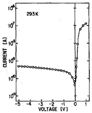
Figure 3-3 shows the typical current-voltage (IV) characteristic in semilog presentation for the undoped a-Si/p-c-Si heterojunction. Two current transport mechanisms are proposed to explain this IVcharacteristic [MATSUURA, 1988].
1. A bulk-limited (space-charge-limited) transport mechanism. 2. A junction-limited current transport mechanism.
The essential difference between (1) and (2) is whether the resistance of the depletion region is greater or smaller than the resistance of the amorphous film. In the bulk-limited case the applied bias drop is mainly across the amorphous layer; in the junction-limited case the applied bias drop is across the depletion region.
Injection of charge carriers into a high resistive interfacial layer results in a gradual transition from ohmic (I°*V) to space charge limited current (SCLC) QocV") characteristics with an increase in forward bias [DUTTA et al., 1995]. At low potentials, as shown in figure 3-3, the TV characteristics are barrier-dominated, but in the high voltage regime, strong injection of excess carriers occurs and the quasi-Fermi level moves through an appreciable energy range towards the corresponding band. The effect of SCLC decreases the effective series resistance above a certain threshold voltage, drastically leading to rapid increase in the current.
A comparison of the TV characteristics of the Schottky diode with and without an amorphous interfacial layer shows an augmentation in the turn-on voltage after the application of the interfacial layer. The turn-on voltage increases further with an increase in the film thickness. In the reverse bias region, the diodes with an interfacial layer exhibit a lower reverse current, and higher breakdown voltage [DUTTA et al., 1995].
-3 -2 "1 0 VOLTAGE tV)
Figure 3-3 Current-voltage characteristics of undoped a-Si:H/p-c-Si (NA = 1016 cm'3)
A theory consistent with a contact barrier diode applying a high resistive interfacial layer is developed as follows [Forrest et al., 1984, Buget et al., 1967]: the current densities for electrons (/„) and holes (Jp) everywhere in the device are given by
Jn=q{lnnE (3-7)
Jp=qjupPE (3-8)
With the total current given by J=Jn+Jp. Here q is the electronic charge, (xn {fxp) is the
mobility of electrons (holes), and E is the electric field. Also, the carrier densities (n,p) are the sum of the equilibrium (no,p0) and injected (ninj,pinj) densities. In the following discussion,
the considered carriers are holes, although similar expressions can be written for electrons. Thus,
P = P0+ Pinj = Nv exp[£v -¥p)lkT\ (3-9)
where Nv is the density of states at the valence band edge (GV), kT is the Boltzmann energy,
and y/p is the quasi-Fermi energy for holes.
Since the conductivity of the interfacial layer is very low, po in this material is small, the Fermi energy is in most cases determined by the density of injected charges, and the transport within the material is space-charge limited.
From current continuity:
dJi=dJJL=dJJL = 0 ( 3_1 0 )
dx dx dx
which is valid at all points within the diode in the absence of charge recombination. From Eq. (3-7), (3-8), and (3-10), and using Poisson's Equation, it can be shown that the electric field in the space-charge layer is
-|l/2
K(MP+Mn)
Where <%=n/p«l, £~0, and ka is the permittivity of interfacial layer. From Eq. (3-11), Esc=0
at the surface of interfacial layer (x-0). Using E=-dV/dx and setting x=d, the current density in the film with thickness d could be expressed by the Mott-Gurney relation:
k a V,2
7 = (9/8) p3 (3-12)
where Vsc is the voltage drop across the space-charge region.
When contact is made between interfacial layer and crystalline substrate, the hole current is limited by thermionic emission over the barrier of height 0Bp. Under reverse bias, the
saturation current in the organic layer (Js) is given by:
Js = -A * T2 exp[- q{<j>Bp - A^) / w ] (3-13)
Here, A* is the Richardson constant, A0 is the image force barrier lowering given by A0 = ijqEm 14nkc , kc is the permittivity of the crystalline substrate, and Em is the electric
field in the substrate at x = d .
Requiring the continuity of both hole and electron currents leads to the familiar expression for thermionic emission across the contact barrier diode:
- 7 =Js{exv[-q(Va-Vsc-VR)/nkT]-l} (3-14)
where n is the diode ideality factor and Va is the applied voltage such that
In the equation above, VD is the voltage drop across the crystalline semiconductor and VR is
the total voltage across the device series resistances (R). Thus
J=VRJ(RA) (3-16)
The thermionic emission SCLC model implies that high electric fields are developed in the crystalline substrate at low current densities, whereas at high currents, the highest fields are in the interfacial thin film. The maximum field in the substrate will be at its surface (x=d) and is given by:
Em=2VD/W (3-17)
And the maximum field in the amorphous layer is estimated using equation (3-11):
/ \ i/ 2
2dJ KM
(3-18)
V'ar-pj
In the preceding discussion, the effect of diffusion and charge trapping on the interfacial layer were neglected. However, traps play an important role in the current transport in amorphous material. It has been shown [Rose, 1963] that the space-charge current in the presence of traps is given by
J = (9/8)kaJueffVs2c'd\ (3-19)
where the effective mobility is //eff = 6>//p. Here,
where pT is the number of trapped holes. The filling of traps reduces the electric field at the interface, which in turn reduces the space-charge-current. The transit time of carriers across the space-charge layer can be estimated using
t - -£— (3-20)
^effuse
CHAPTER 4: EXPERIMENTAL DETAILS 4.1. Preparation of a-SiC
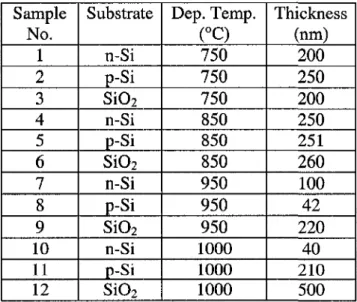
Amorphous SiC thin films were deposited by PSCVD method, using 0.3 g of solid poly dimethylsilane at 1300-2700 Pa above the atmospheric pressure. The details of the PSCVD method have been already reported elsewhere [SCARLETE et al., 2003]. a-SiC films were obtained in few minutes, at maximum deposition-rates of over 250 A/min. Four sets of samples were produced at temperatures of 750 °C, 850 °C, 950 °C and 1000 °C. Faster deposition rates have been obtained at higher temperatures, while the yield of the deposition has not been significantly affected by the temperature. The substrates used were <100>-oriented, n- and p-type silicon single crystal wafers with resistivity in the range of 1-10 Qcm and 1 jitm silicon dioxide thermally grown on Si single crystal wafers. The deposition temperature, substrate and thickness of each sample are presented in Table 4-1.
TABLE 4-1 DEPOSITION CONDITIONS FOR A-SIC THIN FILMS
Sample No. 1 2 3 4 5 6 7 8 9 10 11 12 Substrate n-Si p-Si Si02 n-Si p-Si Si02 n-Si p-Si Si02 n-Si p-Si Si02 Dep. Temp. (°C) 750 750 750 850 850 850 950 950 950 1000 1000 1000 Thickness (nm) 200 250 200 250 251 260 100 42 220 40 210 500
![Figure 2-1 An example of IR spectrum of a-SiC films [MASTELARO et al., 1997]](https://thumb-eu.123doks.com/thumbv2/123doknet/2851410.70633/18.934.268.711.293.624/figure-example-ir-spectrum-sic-films-mastelaro-et.webp)
![Figure 3-1 Models illustrating the structure of (a) crystalline and (b) amorphous materials [MILLER etal., 1991]](https://thumb-eu.123doks.com/thumbv2/123doknet/2851410.70633/31.922.286.732.630.958/figure-models-illustrating-structure-crystalline-amorphous-materials-miller.webp)
![Figure 3-2 Room temperature capacitance voltage characteristics of undoped a-Si:H/p-c-Si (N A = 10 16 cm 3 ) heterojunction [MATSUURA, 1989]](https://thumb-eu.123doks.com/thumbv2/123doknet/2851410.70633/37.923.302.649.140.508/figure-temperature-capacitance-voltage-characteristics-undoped-heterojunction-matsuura.webp)
![Figure 4-1 The arbitrary shaped samples for Hall measurements: (a), (b) acceptable to determine the carrier concentration, carrier type, resistivity, and mobility, (c) recommended only for mobility measurement [Pauw, 1958a]](https://thumb-eu.123doks.com/thumbv2/123doknet/2851410.70633/46.922.220.708.263.542/arbitrary-measurements-acceptable-determine-concentration-resistivity-recommended-measurement.webp)