The dual-gain 10 µm back-thinned 3k x 3k CMOS-APS detector of the
Solar Orbiter Extreme UV Imager
J.-P. Halain
a, A. Debaize
a, JM. Gillis
a, L. Jacques
a, T. De Ridder
b, L. Hermans
b, M. Koch
b, G.
Meynants
b, G. Schippers
ba
Centre Spatial de Liège, Université de Liège, Liege Science Park, 4013 Angleur, Belgium
bCMOSIS, Antwerpen, Belgium
ABSTRACT
The Extreme Ultraviolet Imager (EUI) on-board the Solar Orbiter mission will provide image sequences of the solar atmosphere at selected spectral emission lines in the extreme and vacuum ultraviolet.
For the two Extreme Ultraviolet (EUV) channels of the EUI instrument, low noise and radiation tolerant detectors with low power consumption and high sensitivity in the 10-40 nm wavelength range are required to achieve the science objectives.
In that frame, a dual-gain 10 µm pixel pitch back-thinned 1k x 1k Active Pixel Sensor (APS) CMOS prototype has been tested during the preliminary development phase of the instrument, to validate the pixel design, the expected EUV sensitivity and noise level, and the capability to withstand the mission radiation environment.
Taking heritage of this prototype, the detector architecture has been improved and scaled up to the required 3k x 3k array. The dynamic range is increased, the readout architecture enhanced, the power consumption reduced, and the pixel design adapted to the required stitching. The detector packaging has also been customized to fit within the constraints imposed by the camera mechanical, thermal and electrical boundaries. The manufacturing process has also been adapted and back-thinning process improved.
Once manufactured and packaged, a batch of sensors will undergo a characterization and calibration campaign to select the best candidates for integration into the instrument qualification and flight cameras.
The flight devices, within their cameras, will then be embarked on the EUI instrument, and be the first scientific APS-CMOS detectors for EUV observation of the Sun.
Keywords: Extreme Ultraviolet, Solar Orbiter, camera, detector, APS-CMOS, dual-gain, large scale array,
back-thinning.
1. INTRODUCTION
The Extreme Ultraviolet Imager (EUI) is one of the remote-sensing instrument of the Solar Orbiter mission [1],[2],[3][13]. It
is composed of three channels designed to image the Sun at selected wavelength and appropriate resolution: - A High Resolution Imager (100 km resolution) at the hydrogen Lyman-α line[9] (HRILya channel)
- A High Resolution Imager (100 km resolution) at the Extreme Ultra-Violet (EUV) 174Ǻ line (HRIEUV channel)
- A Full Sun Imager (900 km resolution) at alternatively the EUV 174Ǻ and 304Ǻ lines[4],[5] (FSI channel)
To achieve the science objectives of the EUI instrument, a high sensitivity is required in the 10-40 nm Extreme Ultra-Violet (EUV) wavelength range, for the FSI and HRIEUV channels, and in the visible wavelength range, for the HRILya
channel (an intensifier being glued to the sensor to convert Far Ultra-Violet (FUV) photons into visible photons). These detectors must have a low readout noise (< 5 e-) to allow shutterless operation, but also have a high readout speed (> 1 full frame per second), a radiation tolerance > 40 krad (no charge transfer), a low power consumption (< 1 W), an operational temperature up to -40 °C (low dark current), high dynamic range (full well capacity > 80 ke-), a non destructive readout mode, and windowing capabilities. Additional requirements are imposed by the EUI instrument optical design [11] on the pixel size (10 µm) and large format (3k x 3k).
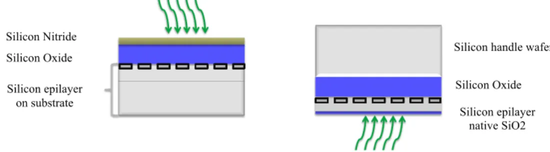
A dedicated dual-gain Active Pixel Sensor (APS) CMOS pixel on a Silicon-On-Insulator (SOI) material has been developed to achieve these objectives. The pixel is readout through a high gain (HG) and a low gain (LG) path to improve the dynamic range. The pixel associated capacitance to low and high gains determine the sensitivity of the pixel (low readout noise in the HG and high full well in the LG). A front-side illuminated version of the sensor is used for the visible range sensitivity. For the EUV range, where the penetration depth of photons in silicon (Si) limits the sensitivity, a backside illuminated version is used, with thinning of the epitaxial Si layer (Figure 1). The SOI allows to obtain a thin and uniform Si layer (the buried oxide acts as an etch stop layer). The epitaxial Si layer is thinned down to 3 µm after substrate and buried oxide removals. For mechanical stability, a Si handle wafer is attached to the front side of the SOI.
Figure 1 – Front side (left) versus back side (right) imager.
A 1k x 1k prototype of this detector has been tested during the preliminary development phase of the EUI instrument, to validate the pixel design, the expected EUV sensitivity, the noise level, and the capability to withstand the mission radiation environment. The detector architecture has then been scaled up (using stitching) to the required 3k x 3k array with a custom detector package compatible with the EUI camera constraints.
2. EUI CAMERAS
The EUI cameras are based on a 3k x 3k 10 µm pitch CMOS-APS detectors (windowed to 2k x 2k in the HRI camera). The three EUI cameras share a common electrical,
mechanical and thermal design concept, based on a common detector (3k x 3k CMOS APS) thermally decoupled from the camera housing and boards. Each camera is adapted to the constraints of its position within the OBS unit (allocated volume, position w.r.t. thermal interface with spacecraft…). Figure 2 shows the FSI camera [17]. The detector is
thermally decoupled from the camera, but connected to the EUI instrument bench and thermal interface of the spacecraft.
Figure 2 – EUI FSI camera
3. PROTOTYPE DETECTOR
The EUI detector prototypes (named APSOLUTE for APS Optimized for Low-noise and Ultraviolet Tests and Experiments) consist in two image sensors (Figure 3) made in 0.18 µm CMOS process with SOI material, and procured by the CMOSIS Company [10][12].
- A 256 x 256 pixel array with 16 pixel variants organized in blocks of 64 x 64 pixels. - A 1024 x 1024 pixel array containing the best guess pixel variant out of the 16 variants.
The objective of the 16 pixel variants is to select the best pixel design variant for flight detectors. The 1k x 1k is close to the flight model size and was built to validate the manufacturing process (in particular back thinning) and derive performances on a large-scale device.
Silicon Nitride Silicon Oxide Silicon epilayer
on substrate
Silicon handle wafer Silicon Oxide
Silicon epilayer native SiO2
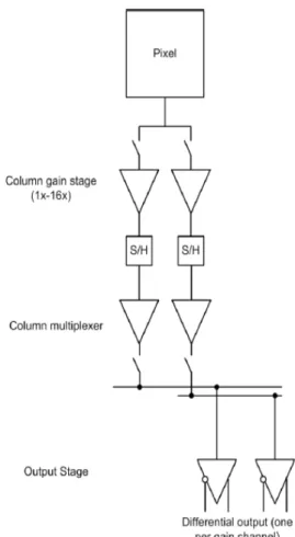
In both cases, the pixels (and the rolling shutter) are controlled by off-chip signaling through the pixel control block. To achieve the requested high dynamic range, two gain paths are available per pixel. This results in 2 x N outputs per line of N pixels. 2 x N column gain stages are implemented. Each column multiplexer sends 2 x N data to a single analog output channel. The output stage converts the signal to a fully-differential signal which can be sent to an off-chip A/D converter. An SPI interface is used to control various sensor settings (bias currents, voltage levels, gains …) and a temperature sensor is read out over the SPI interface.
A back and a front side prototype of the APS detector have been developed and characterized to validate EUV and visible sensitivity and impact on the pixel performances [10]. The
prototype detectors were tested in a dedicated EGSE for powering and acquiring images. The tests that were conducted include flat field and MTF measurement, dark current characterization versus temperature, photon transfer curve (PTC) characterization, EUV response [14]. These tests were performed
before and after radiation hardness tests, i.e. Total Ionizing Dose (TID), Heavy Ions (HI) and Protons irradiation [15][16].
Figure 3 – APS prototypes (left: 1k x 1k, right: 256 x 256) developed to validate the EUI detector
baseline
The prototype demonstrated the feasibility of the specification for the flight-model detector and the suitability of the CMOS-APS technology for EUI instrument. The flight model detector with analog output can be extrapolated straight forward from the prototype sensor. It also provides some lessons for the flight model development (pixel improvements, back-thinning processing impact, etc). In particular the backside processing of the flight detectors will be further optimized with respect to achieving lower dark current and tolerance to EUV damage.
4. FLIGHT DETECTOR
The 3k x 3k flight detectors are stitched device and are based on the architecture presented in Figure 5, derived from the APSOLUTE prototype. It is also based on the SOI material with 0.18 µm CMOS process. Two output gains are implemented per pixel to achieve a low readout noise and a high full well. The outputs are multiplexed and externally converted to digital signal. For use as a 2k x 2k in the HRI cameras, windowing in X and Y is implemented.
The number of columns included 4 optical dummy columns (2 on each side). The optical dummy columns are terminated after the column load so they cannot be read. On top and bottom there are also 2 optical dummy rows. On the bottom these are 2 modified pixel rows for black sun protection. The total number of pixels is thus 3074 x 3076 and the useful image size array is 3072 x 3072. 6144 The large array imposed to consider stitching for manufacturing reasons.
Figure 4 – EUI flight detector pixel architecture (top) and layout (bottom) – 0.18 µm CMOS technology
The pixel design was derived from the best one of the APSOLUTE prototype. A 6-transistor double transfer gate with single output channel was selected (Figure 5). The layout of the selected pixel was also modified to be compatible with backside thinning and avoid hot pixel clusters.
To be able to achieve the high dynamic range of 84dB (< 5e-noise for a full well charge of > 80 ke-) each pixel is read out over two gain paths. A first gain of 6.5x is already applied in the pixel (by the two conversion gains). A gain of 4 x in the column gain stage implements a total gain of almost over 24 x for the ‘high gain path’. For the ‘low gain path’ the column gain should be set to 1x. As on the prototype sensor 2N gain stages are used for the N pixels (2 gains per pixel: high gain and low gain) (see Figure 6). The gain in the column is adjustable up to 16x and it can be set separately for each of the two channels. The high and low gain samples are output at different times. The amplified pixel signal and reset samples from both high and low gain paths are stored in the Sample-and-Hold (S/H) stages. The column amplifiers for high and low gain are identical, but they are operated with a different. From this point in the data path onwards high and low gain paths are identical in timing and all programmable settings. The sample-and-hold capacitors are read out by the column multiplexer which feeds the pixel signals to the output stage sequentially. The output stage outputs the signal as a fully-differential signal which can be sent to an off-chip A/D converter. The pixel samples are logically ordered in the outputs (from one
sensor edge to the other edge). Figure 6 – Analog path architecture (high and low gain multiplexer bus) The frame timing controls the major functions of the sensor:
- Control the electronic rolling shutter: start and stop integration of light on the pixel. - Read out the integrated image over the analog outputs.
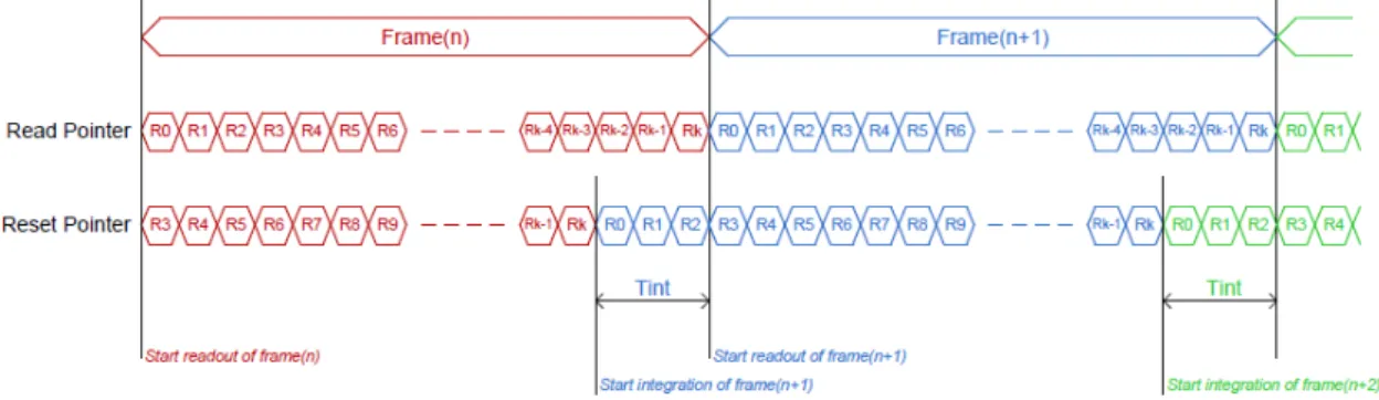
Controlling the rolling shutter and reading out the image data from the sensor is row-based. This means that the image frame can be split up in a number of rows as shown in Figure 7. To read out an image, a total of 3072 pixel rows need to be read. Each pixel row contains 6144 analog data samples, two for each pixel (dual gain path). Both gain paths are handled in parallel. Optionally a number of dummy rows can be added to these 3072 pixel rows. The reason for these dummy rows is to extend the maximal integration time. The bigger the number of dummy rows, the longer the frame time and as such the lower the frame rate will be. The maximal frame rate is achieved when the number of dummy rows is zero.
During each pixel row or dummy row, the integration of light on a single pixel line in the array can be initiated, meaning that the shutter for that line is opened. Also, during each pixel row, the integration of light on the according pixel line in the array is stopped, meaning that the shutter on that line is closed. Figure 8 illustrates the rolling shutter timing with an example. The example in Figure 8 shows the frame timing for an integration time of 3 row times. The figure makes clear that two line address pointers are required: one points to the pixel line to be read, the other one points to the pixel line to be reset. To achieve an integration time of 3 rows as illustrated in the figure, the reset pointer is preceding the read pointer by 3 counts. Without dummy lines, this means that the integration of the first line of frame (n+1) starts while reading line 3069 (k=3071 for 3k x 3k) of frame (n). To increase / decrease the integration time, the difference between both pointers must be increased / decreased. Without dummy rows, as illustrated, the maximum integration time is limited to 3071 row times. To further increase the integration time, dummy rows must be added to the frame time. Adding these dummy rows is purely accomplished by external timing.
Figure 8 – Illustration on controlling the integration time of the rolling shutter The expected performances of the EUI flight
detector are summarized in Table 1 and Table 2. The expected noise versus integrated electrons is plotted inFigure 9
.
The red curve represents the input referred noise of the low gain path, the green curve represents the input referred noise of the high gain path. As an example, also a simulation is done with the column gain of the high gain path set to 16x, represented by the purple curve. It is clear that there is not a big advantage for the dark noise level, while the noise ‘step’ between the high and low gain signals becomes much bigger. This noise step corresponds to a step in the signal-to-noise ratio, which can be visible in the image if the step is too large. The reason that a higher gain is not very advantageous is that the noise is dominated by the first noise source in the path,
namely the pixel source follower. Figure 9 – Noise chart of the EUI flight detector A temperature sensor is included in the die and can be read out as a voltage difference between 2 analog outputs.
Table 1 – EUI flight detectors expected overall performances
Overall parameter Expected value
Pixel 10 µm pitch
Array 3k x 3k array (stitched) with X/Y windowing Maximum pixel rate (frame rate) > 1 frame per second (faster with windowing)
Overall parameter Expected value Sensitivity (detected ph/incident ph) > 50% at 17.4 nm and 600 nm
Average dark signal 10 e-/s/px (at -40 °C)
Non-linearity (p-p) < 2%
Power consumption 0.85 W
Radiation hardness > 40 krad (on back-side)
Table 2 – EUI flight detectors expected noise performances
Parameter (after output stage) Low gain path High gain path
Signal noise 0.604 mV 1.19 mV Conversion gain 14.4 µV/e- 374 µV/e- Saturation charge > 80 ke- 4800 e-
Readout noise 40 e- 3 e-
5. DETECTOR PACKAGE
The FM detector package is made of Aluminium Nitride (AlN) ceramic to match with the thermo-elastic coefficient (CTE) of the silicon die and to provide relatively high thermal conductivity (150 W/mK) for a limited mass (0.08 kg per package). To reduce absorptivity and limit heat exchange from the camera, the package will also be gold coated.
The package of the FSI and HRIEUV detectors is
mechanically supported in the camera by Titanium blades, and thermally connected to cooling straps (Figure 11). In the HRILya channel,
the package is fixed to the camera via the intensifier mechanical interface.
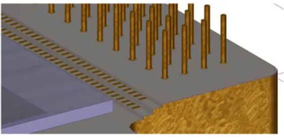
The wire bonding from the die are routed through the AlN package (Figure 10) and they are electrically connected to the camera front-end electronic by a two layers flex and miniaturized connector (Figure 12). The connector has the main advantage of allowing dismounting in case of any issue during the tests of the camera.
Figure 10 – Wire bonding routing through the AlN package
A thermal model of the detector assessed that the material thickness provides sufficient temperature homogeneity over the die surface. An homogeneity of ~ 1 °C is achieved, with 1 W applied on the read-out circuitry of the detector.
Figure 11 – EUI FM detector package (left: for the FSI and HRIEUV channels, right: for the HRILya with additional Titanium
cap for intensifier gluing)
Figure 12 – EUI detector flex connecting package to camera connector Cover for intensifier gluing Thermal strap 3k x 3k die Flex
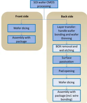
6. DETECTOR MANUFACTURING AND PROCESSING
The flight models of the EUI detectors have been tape out. The manufacturing flow of the die includes the following steps. For the front-side die (visible sensitive detectors), the EUV related steps are skipped, as shown on Figure 13. - SOI wafer CMOS processing (0.18 µm CIS
process).
- Back-side processing
o Layer transfer and wafer-to-wafer bonding. o Handle wafer thinning.
o To be EUV sensitive, original oxide is removed (BOX removal) by wet etching. EPI can also be etched to remove the sensitivity loss due to the dead-zone. o To improve dark current and limit
degradation by the EUV photons, an additional surface passivation is performed. o Bonding pad opening
- Wafer dicing
- Assembly of the die with the detector package and interconnecting flex, including the wire bonding to the package finger pads.
SOI wafer CMOS processing Front side Wafer dicing Back side Layer transfer: handle wafer bonding and wafer
thinning BOX removal and
wet etching Surface passivation Pad opening Wafer dicing Assembly with package (incl. wire
bonding) Assembly with
package
Figure 13 – EUI detector manufacturing and processing flow (back-side device)
7. CONCLUSIONS
Taking heritage of a detector prototype developed and tested as part of the EUI instrument preliminary phase, the flight detector has been designed and its architecture improved for the required instrument performances. The detector packaging has also been customised to match with the instrument constraints.
Once manufactured, a first batch of front side devices will be functionally tested and characterized in the visible light to select the best candidate for the HRILya flight model camera. They will also serve to validate the electrical design of the
camera. A second batch of devices will be back-thinned and best candidates for FSI and HRIEUV cameras will be selected
and characterized in the EUV. The remaining devices (front and back side) will serve for the EUI instrument Qualification Model (QM) and for radiation validations of the detectors.
ACKNOWLEDGEMENTS
The EUI instrument is developed in a collaboration which includes the Centre Spatial de Liège (Belgium), the Institut d’Astrophysique Spatiale and the Institut d’Optique (France), the UCL Mullard Space Science Laboratory (UK), the Max Planck Institute for Solar System Research (Germany), the Physikalisch-Meteorologisches Observatorium Davos (Switzerland), and the Royal Observatory of Belgium (Belgium).
The Belgian institutions are funded by Belgian Federal Science Policy Office (BELPSO); the French institutions by Centre National d'Etudes Spatiales (CNES), the UK institution by the UK Space Agency (UKSA); the German institution by Deutsche Zentrum für Luft- und Raumfahrt e.V. (DLR), and the Swiss institution by the Swiss Space Office (SSO).
The CMOSIS Company, located in Antwerpen, Belgium, is responsible of the detector development; under the ESA-PRODEX contract no. 4000110352.
REFERENCES
[1] Fleck B., Harrison R. A., Marsden R. G., Wimmer-Schweingruber R., “Summary of the Solar Orbiter payload working group activities, Telescopes and Instrumentation for Solar Astrophysics” Proc. SPIE 5171, 123-130, (2004).
[2] Marsden R.G., Marsch E. and the Solar Orbiter Science Definition Team, “Solar Orbiter Science Requirements Document” SCI-SH/2005/100/RGM Issue 1 Revision 2, (2005).
[3] Mc Coy D., and the Solar Orbiter assessment team, “Solar Orbiter Payload Definition Document” SCI-A/2004/175/AO Issue 5 Revision 0, (2006).
[4] Rochus P., Halain J.P., Renotte E., Berghmans D., Zhukov A., Hochedez J.F., Appourchaux T., Auchère F., Harra L.K, Schühle U., Mercier R.., “The Extreme Ultraviolet Imager (EUI) on-board the Solar orbiter Mission” 60th International Astronautical Congress, (2009).
[5] Hochedez J.-F., Appourchaux T., Defise J.-M., Harra L. K., Schuehle U., Auchère F., Curdt W., Hancock B., Kretzschmar M., Lawrence G., Marsch E., Parenti S., Podladchikova E., Rochus P., Rodriguez L., Rouesnel F., Solanki S., Teriaca L., Van Driel L., Vial J.-C., Winter B., Zhukov A., “EUI, The Ultraviolet Imaging Telescopes of Solar Orbiter” The Second Solar Orbiter Workshop, (2006).
[6] Halain J.-P., Rochus P., Appourchaux T., Berghmans D., Harra L., Schühle U., Auchère F., Zhukov A., Renotte E., Defise J.-M., Rossi L., Fleury-Frenette K., Jacques L., Hochedez J.-F., Ben Moussa A., "The technical challenges of the Solar-Orbiter EUI instrument” Proc. SPIE 7732, 26, (2010)
[7] Halain J.-P., Berghmans D., Defise J.-M., Renotte E., Thibert T., Mazy E., Rochus P., Nicula B., De Groof A., Seaton D., Schühle U., “The First light of SWAP on-board PROBA2” Proc. SPIE 7732, 24, (2010)
[8] Auchère F., et al., "HECOR, a HElium CORonagraph aboard the Herschel sounding rocket" Proc. SPIE 6689, (2007)
[9] Schühle U., Halain J., Meining S., Teriaca L., "The Lyman-alpha telescope of the extreme ultraviolet imager on Solar Orbiter" Proc. SPIE Solar Physics and Space Weather Instrumentation IV, 8148, (2011)
[10] Halain J.-P., Rochus P., Renotte E., Appourchaux T., Berghmans D., Harra L., Schühle U., Schmutz W., Auchère, F., Zhukov A., Dumesnil C., Kennedy, T., Mercier R., Pfiffner D., Rossi L., Tandy J., Smith P., “The EUI instrument on board the Solar Orbiter mission: from breadboard and prototypes to instrument model validation” Proc. SPIE 8443, (2012)
[11] Halain J.-P., Mazzoli A., Rochus P., Renotte E., Stockman Y., Berghmans D., Benmoussa A., Auchère F., “EUV high resolution imager on-board Solar Orbiter: optical design and detector performances”, International Conference on Space optics ESA, (2012)
[12] Wang X., Wolfs B., Bogaerts J., Meynants G., BenMoussa A; “A high-dynamic range (HDR) back-side illuminated (BSI) CMOS image sensor for extreme UV detection” Proc. SPIE 6413, (2012)
[13] Fahmy S., Bagnasco G., Pacros A., Wirth K., “Solar Orbiter payload suite: a hotbed of innovation” 64th International Astronautical Congress IAC-13-A3.5.2, 2013
[14] A. BenMoussa, B. Giordanengo, S. Gissot, G. Meynants, X. Wang,B. Wolfs, J. Bogaerts, U. Schuhle, G. Berger, A. Gottwald, C. Laubis, U. Kroth, F. Scholze, “Characterization of Backside-Illuminated CMOS APS Prototypes for the Extreme Ultraviolet Imager On-Board Solar Orbiter” IEEE Transactions on Electron Devices, 60(5),1701-1708, (2013)
[15] Ali BenMoussa, A. Soltani, C Gerbedoen, T. Saito, S. Averin, S. Gissot, B. Giordanengo, G. Berger, U. Kroth, J-C. De Jaeger, A. Gottwald, “Developments, characterization and proton irradiation damage tests of AlN detectors for VUV Solar Observations” Nuclear Instruments and Methods in Physics Research Section B Beam Interactions with Materials and Atoms, 312:48-53, (2013)
[16] Ali BenMoussa, S. Gissot, B. Giordanengo, G. Meynants, X. Wang,B. Wolfs, J. Bogaerts, U. Schühle, G. Berger, A. Gottwald, C. Laubis, U. Kroth, F. Scholze, A. Soltani, T. Saito, “Irradiation Damage Tests on Backside-Illuminated CMOS APS Prototypes for the Extreme Ultraviolet Imager On-Board Solar Orbiter” IEEE Transactions on Nuclear Science; 60(5), 3907 – 3914, (2013)
[17] Halain J.-P., Rochus P., Renotte E., Auchère F., Berghmans D., Harra L., Schühle U., Schmutz W., Zhukov A., Aznar Cuadrado R., Delmotte F., Dumesnil C., Gyo M., Kennedy T., Mercier R., Verbeeck C., Thome M., Heerlein K., Hermans A., Jacques L., Mazzoli A., Meining S., Rossi L., Tandy J., Smith P., Winter B.., “The Extreme UV Imager of Solar Orbiter – From detailed design to Flight Model” Proc. SPIE 9144, (2014)