O
pen
A
rchive
T
oulouse
A
rchive
O
uverte (
OATAO
)
OATAO is an open access repository that collects the work of Toulouse researchers and makes it freely available over the web where possible.
This is an author-deposited version published in: http://oatao.univ-toulouse.fr/
Eprints ID: 577
To cite this document: RISSONS, Angélique. MOLLIER, Jean-Claude. Critical study of the vertical-cavity surface emitting laser electrical access for integrated optical sub-assembly. In:
EMC Europe Workshop,
11-12
juin 2009
,Athènes, Grèce
,pp.1-2
.Any correspondence concerning this service should be sent to the repository administrator: [email protected]
a
. Title: Critical study of the Vertical-Cavity Surface Emitting Laser Electrical Access for integrated optical sub-assemblyb. Authors : Angélique Rissons, Jean-Claude Mollier
c. Affiliation : DEOS, Institut Supérieur de l’Aéronautique et de l’Espace (ISAE), Université de
Toulouse, France
d. Keywords: Optical Interconnection, Optoelectronic S-Parameters, small-signal equivalent circuit,
crosstalk .
e. Introduction :
To satisfy the rise of bandwidth, the optical links have found their place in the high bit rate communication field. According to the emergence of the short distance optical communication, the Vertical-Cavity Surface Emitting Laser (VCSEL) became, in the last ten year, a key component of the optical interconnection. Indeed, the numerous advantages of this component make the VCSEL technology competitive face to the Edge Emitter Laser (EEL) and the Light Emitting Diode (LED): providing the laser performance while keeping a cost effectiveness. Above all, the VCSEL has been designed to achieve the need of the planarization of optoelectronic circuits. Since its invention at the end of the 70th by Prof. K. Iga and its first commercialization at the end of the 90th, the VCSEL structure is in a state of constant progress. Today, a wide wavelength emission range (from the Green-blue band up to the infrared) is covered that enable the usage of these components in various applications, not only in the field of digital communications (Gigabit Ethernet) but also in consumer applications (laser printers, laser mice, display systems, etc.). All these applications are due to the following features: laser emission perpendicular to the layers making easy the one or two dimensional integration, smallest laser diode type, higher integration level low electrical power consumption, low thermal variation close to the room temperature, serial fabrication and circular light beam.
All these reasons have led the growth of the VCSEL market in a wide application range especially in the integrated optical sub-assembly for optical interconnections [1]. Despite of the integration facilitated by the vertical structure, the electrical access allowing the drive of the VCSEL need to be optimized in order to match the VCSEL with its driving circuit. In this way, an optoelectronic modelling of various VCSEL chip is proposed. The model is based on the comparison of a small signal electrical circuit of the VCSEL with its electrical access and the VCSEL rate equations so as to set up relationships between laser intrinsic parameters and the equivalent circuit elements.
The circuit elements are deduced from the scattering parameters of various VCSEL chip submount: microstrip and wire bonding or direct coplanar access. Various experiments prove the effect of the electrical access on the laser response for modulation frequency above 1GHz. The discussion of the different experimental results provides a critical comparison of the different VCSEL submount especially in term of electrical access.
f. The approach consist in describing the physical phenomena occurring into the VCSEL structure by an equivalent circuit. This concept has been proposed by R.S Tucker [2] for EEL. As the electronic funneling through the VCSEL structure is different than the EEL one, the electrical equivalent structure needs to be adapted to the VCSEL by including the multi-quantum well active layer represented by a RLC resonant circuit and the doped Distributed Bragg Reflector (stack of doped heterojunctions) equivalent to distributed RC cells. This behavioral electrical equivalent circuit is cascaded with the electrical access according to each submount (figure 1).
To write the relationship between VCSEL intrinsic parameters and the circuit element, the resolution of the rate equations is required. The laser rate equations are two coupled rate equations in which the electrons and photons interactions are converted into mathematic form: the carrier rate equation is the difference between the carrier injection with the recombination rate (non-radiative and radiative), the photon rate equation is the difference between the photon generated which can be amplified by stimulated emission and the lost photons. After a linearization of the rate equation with small signal approximation, we can easily define relationship between intrinsic parameters and circuit elements. The second step of this study is the extraction of the circuit element through the measurement of the scattering parameters of the VCSEL chip. The measurement of the electrical reflection coefficient and the optoelectronic coefficient is achieved by using a HP 8510 Vector Network Analyzer.
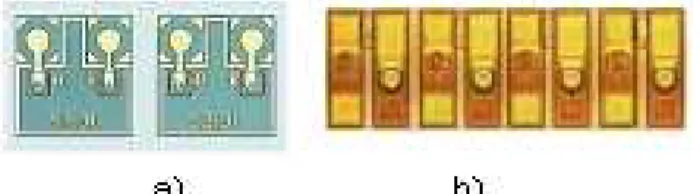
Figure 1: a) VCSEL array with a microstrip access b) VCSEL array with a coplanar access.
The experimental setup depends on the VCSEL structure (three different emitting wavelength: 850nm, 1310nm and 1550nm) and the electrical access (the VCSEL array presented on the Figure 1. b could be directly tested by using GSG RF probe, the VCSEL array of the figure 1.a need to be mounted on a ceramic submount to be tested on the probe station). Contrary to the other laser diode previously tested [2], we exclude the test on typical TO packaged VCSEL to avoid the parasitic effects induced by the package. The model is validated by comparing the measurement and the S-parameters simulation by using ADS TM.
g. All achieved test highlight the consequence of a non adapted packaging for the optical subassembly
of an optical interconnection module. Indeed, two kinds of results are obtained. The S11 and S21 measurement of the VCSEL array mounted on ceramic are strongly disturbed. Moreover, a coupling between two adjacent VCSELs from the same array was easily observed: when one VCSEL was modulated, the neighbour VCSELs lased without any injected current. In fact, the distances between the VCSEL electrical accesses are so small that the RF modulation through the coplanar line and the bond wire could circulate on the neighbouring channels. We assume that the crosstalk is due to the wire bonding can be neglected and the access. The electrical crosstalk can be introduced in the electrical equivalent circuit as a mutual inductance, a capacitance and a resistance between both channels. The characterization and modelling of this crosstalk is presented on the figure 2 and show that the electrical crosstalk is not significant below 1GHz (less than –35dB) and it increases quickly above this frequency. The second kind of measurement is obtained on coplanar access VCSEL array. The results are consistent up to 10GHz, but when we extend frequency range up to 20GHz, the S21 of the VCSEL is not conform to a typical laser response involving another effect of the electrical access. This effect appears on the longwavelength VCSEL but not on the 850nm VCSEL. The modelling of this effect using the transfer matrix formalism is currently in progress.
Figure 2: crosstalk measurement (blue curve) and simulation ( red curve) of a VCSEL array.
h. References:
[1] K.S. Ly, A. Rissons, F. Quentel, M. Pez, E. Gambardella, J-C Mollier, « Bidirectional link Mock-Up For Avionics Applications”, IEEE Conference on Avionic FiberOPtic (AVOP), Sandiego , CA, September 2008. [2]Rodney S. Tucker and David J. Pope, “Microwave Circuit Models Of Semiconductor Injection Lasers”, IEEE Transactions On Microwave Theory And Techniques, Vol. MTT-31, No.3, March 1983.
[3]S. Nakagawa, S-Y Hu , D. Louderback, L. Coldren, “R.F. Crosstalk in Multiple-Wavelength Vertical-Cavity Surface Emitting Laser Arrays”, IEEE Photonics Technology Letters, VOL. 12, NO. 6, June 2000.