Science Arts & Métiers (SAM)
is an open access repository that collects the work of Arts et Métiers Institute of Technology researchers and makes it freely available over the web where possible.
This is an author-deposited version published in: https://sam.ensam.eu Handle ID: .http://hdl.handle.net/10985/10088
To cite this version :
Andriy VASIN, Yuri GOMENIUK, Audrey RUSAVSKY, Alexey N. NAZAROV, V.S. LYSENKO, Petro M. LYTVYN, O.G. GONTAR, Sergii P. STARIK, Corinne NOUVEAU, S. ASHOK - Nano-and micro-scale morghological defects in oxidized a-SiC: H thin films - Physica Status Solidi (C) Current Topics in Solid State Physics - Vol. 10, n°4, p.619-623 - 2013
Any correspondence concerning this service should be sent to the repository Administrator : [email protected]
Nano- and micro-scale morghological
defects in oxidized a-SiC:H thin films
A. V. Vasin*,1, Y. Y. Gomeniuk1, A. V. Rusavsky1, A. N. Nazarov1, V. S. Lysenko1, P. M. Lytvyn1, O. G. Gontar, S. P. Starik2, C. Nouveau3, and S. Ashok4
1 Lashkaryov Institute of Semiconductor Physics, Kiev 03028, Ukraine
2 Bakul Institute of Superhard Materials, 2 Avtzavodskaya str., Kiev 04074, Ukraine 3 LaBoMaP, CER Arts et Métiers ParisTech, Rue Porte de Paris, 71250 Cluny, France
4 The Pennsylvania State University, 212 Earth and Engineering Science Building, University Park, PA 16802, USA
Received 15 October 2012, revised 4 December 2012, accepted 12 December 2012 Published online 11 March 2013
Keywords amorphous SiC films, oxidation, morphological defects
* Corresponding author: e-mail [email protected], Phone: +380 44 525 6395, Fax: +380 44 525 6177
Amorphous carbon rich a-SiC:H films were deposited on silicon substrates by RF-magnetron sputtering of SiC tar-get in argon/methane gas mixture. The principal focus of this study was investigation of the effect of thermal oxidation on structure and morphology reconstruction in a-SiC:H amorphous network. The density of the films was varied over the range 1.6-2.2 g/cm2 by varying the magnetron discharge power. The local nano- and micro-scale surface morphology and chemical composition dis-tribution were examined by atomic force microscopy, scanning electron microscopy equipped with Auger
elec-tron scanning system and optical profilometry. It was found that partial oxidation leads to local structure recon-struction accompanied by transformation of mechanical stresses from compressive to tensile. Formation of car-bon-enriched nano- and micro-scale regions was ob-served after oxidation in low density samples. We attrribute these morphological defects to migration and precipitation of carbon species released in the process of oxidation of the SiC amorphous network. The mecha-nism of tensile stresses generation is also discussed.
1 Introduction Silicon carbide is a widely used
mate-rial due to excellent combination of electronic properties, mechanical strength and chemical inertness. Crystalline silicon carbide (SiC) is a basic material in high temperature and high power electronic devices. In polycrystalline form, it finds application as an abrasive and wear-resistant mate-rial in mechanical tool applications. As biocompatible ma-terial, silicon carbide has been recognized as a prospective material for orthopedic devices and biomedical micro-electro-mechanical-systems (MEMS) implantable in living tissue [1–5]. The main disadvantage of the crystalline SiC materials is the high temperature for synthesis.
Amorphous hydrogenated silicon carbide thin film (more correctly “hydrogenated amorphous silicon-carbon alloy” films or a-SiC:H) grown at low temperature attract attention as a prospective substitute for the crystalline counterpart in some of application areas. a-SiC:H can be deposited as a smooth and uniform layer on large area sur-faces at substrates temperatures as low as 200 oC. Me-chanical and chemical properties of amorphous material
are strongly dependent on composition, nanoscale structure and growth morphology determined by physico-technological conditions of the deposition process. Due to the thermodynamically non-equilibrium of low tempera-ture growth conditions, the amorphous material contains significant morphological and structural defects.
Corrosion resistance is one of the advantages of silicon carbide. Oxidation behavior of amorphous SiC material is expected to be strongly different from that of bulk crystal-line SiC material due to reduced density and chemical dis-order. It has been demonstrated that corrosion resistance of the hydrogenated a-SiC:H films is lower than in unhydro-gentaed a-SiC layers [6]. One of the main reason of low corrosion resistance of a-SiC:H layer is nanoporousity as-sociated with bonded hydrogen. On the other hand, the hy-drogenated nanoporous structure of a-SiC:H material re-sults in reduced mechanical stresses that is very important in applications where adhesion stability is a critical issue.
The present work is focused on the study of oxidation behavior of a-SiC:H films deposited by RF magnetron sputtering of SiC target.
2 Experimental
The a-SiC:H layers were deposited on boron doped Si(001) 10 Ω cm wafers by RF-magnetron sputtering of 160 mm diameter crystalline SiC target using Ar(93 vol.%) + CH4(7 vol.%) mixture as a working gas at different dis-charge powers. Such a deposition system allows formation of SiC films with wide-ranging density by varying the RF-discharge power. Measurements show that increasing the discharge power from 180 W to 330 W increased the film density from 1.6 g·cm3 to 2.2 g·cm3.
The nominal thickness of the films was about 300 nm. All samples contain overstochiometric carbon incorpora-tion (about 60 at.%). Excess of carbon obviously comes from methane diluted in argon, as we used stochiometric crystalline SiC target for sputtering. After the deposition the samples were annealed at atmospheric pressure in flow of oxygen at temperature 550 oC and 650 oC for 30 min. After thermal treatment the samples were examined by Fourier-transform infra-red (FTIR) transmission spectros-copy, scanning electron microscopy (SEM), Atom force microscopy (AFM), Kelvin probe force microscopy (KPFM), Raman scattering spectroscopy, and optical pro-filometry.
3 Results and discussion
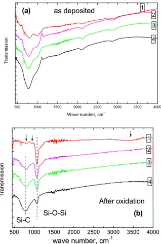
FTIR transmission spectra of as-deposited and ther-mally treated samples are presented in Fig. 1. Spectra of as-deposited samples (Fig. 1(a)) are composed of four main absorption bands typical for a-SiC:H layers: 800 cm-1 (Si–C stretching), 1000 cm-1 (Si:C–H
2 bending), 2100 cm-1 (Si–Hn stretching), and 2800–3000 cm-1 (C–Hn stretching) [7, 8]. In the 1000–1100 cm-1 region some contribution to the absorption due to oxygen contamination is expected.
I is evident from the figures that the principal effect of increase in discharge power is increase of the relative intensity of the Si-C related absorption band at 800 cm-1, in comparison with the hydrogen related band at 1000 cm-1. It can be interpreted as increase of the concentration of Si-C bonds and decrease of SiC-Hn associated mainly with hydrocarbon radicals in the nano-voids. Such interpretation is in good agreement with increase of the density of the films observed with increasing of discharge power.
The FTIR spectrum of the sample after oxidation in O2 atmosphere at 550 oC is presented in Fig. 1(b). No Si–H
n (2100 cm-1) and C–H
n (2900–3000 cm-1) stretching vibra-tion bands were detected after dry oxidavibra-tion. In the spec-trum of the sample deposited at lowest discharge power (i.e. lower density of the material) there are four pro-nounced absorption bands at 446 cm-1, 805 cm-1, 945 cm-1, 1070 cm-1 (with shoulder at 1200 cm-1) all of which known to be related to oxygen bonds: Si-O-Si (symmetrical stretching), Si-OH (stretching), Si-O-Si (asymmetrical
stretching), and O-H (stretching) respectively. One can see that relative intensity of the main silicon-oxygen absorption bond (1070 cm-1) is reduced as the density of the film increases.
Figure 1 FTIR transmission spectra of as-deposited (a) and
oxi-dized (550 oC) a-SiC:H samples deposited at RF-discharge power of 180 W (1), 200 W (2), 250 W (3), and 330 W (4).
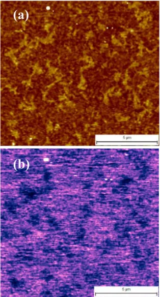
The analysis of the film surface by AFM and SEM revealed formation of (1) nano- and (2) micro-scale morphological defects after oxidation treatment of the samples deposited at low discharge power. We will show that these defects are related to migration and redistribution of carbon released after oxidation of the amorphous SiC matrix.
3.1 Nano-scale defects Atomic force microscopy
measurements show that surface of as-deposited films is smooth and uniform. But after oxidation of the low density sample (the sample deposited at lowest discharge power, see spectrum 1 in Fig. 1) at 550 oC we observe formation of island-like inhomogenities (Fig. 2(a)). Such morpho-logical defects were not observed after oxidation at 650 oC. IR spectra of these samples (not presented here) do not differ significantly. The size of island-like morphological
500 1000 1500 2000 2500 3000 3500 4000 4 3 2 T ransmission Wave number, cm-1 as deposited (a) 1 500 1000 1500 2000 2500 3000 3500 4000 4 3 2 Si-C Transmission wave number, cm-1 Si-O-Si 1 (b) After oxidation
defects ranges from several hundred nm to several µm, and islet defects protrude above the surface of the main body of the films by about 10 nm.
Figure 2 (a) AFM topology (contrast of height in range of
10 nm) and (b) KPFM map (contrast of surface potential in range of 30 mV) of the surface of low density a-SiC:H films after oxi-dation at 550 oC.
Kelvin probe force measurements exhibit that the surface potential of the defects is significantly lower than that of the surrounding matrix (Fig. 2(b) indicating that electrical properties of the material is also inhomogeneous.. To identify the origin of these defects the surface was examined by scanning electron microscopy combined with local high resolution Auger electron spectroscopy (JAMP-9500 F).
Figure 3 shows the SEM image generated by secondary electrons of the surface of the sample after annealing in oxygen at 550 oC (Fig. 3(a)) and the corresponding distribution of carbon on the surface of the
sample (Fig. 3(b)). It is seen that carbon distribution replicates the morphological map, thus indicating that the island-like defects are enriched by carbon in comparison with the surrounding surface. Local nano-probe measurements show that the flat surface contains much more oxygen than island-like defects. Thus island-like defects can be attributed to non-oxidized regions.
Figure 3 SEM (regime of secondary electron detection) image
(a) and carbon distribution map generated by Auger-electron scanning probe (b) of the low density sample after oxidation at 550 oC. Contrast of carbon distribution map corresponds to the range from background signal of the C(KVV) line (black) to maximum of the amplitude of C(KVV) line (white).
In FTIR spectrum of this sample (Fig. 1, spectrum 1) we see only silicon oxide related absorption bands so we can say the a-SiC material is “completely oxidized”. IR ab-sorption cross section of Si-C and Si-O bonds is different but of the same order. From the surface image we see that relative contribution of the volume of island-like regions is quite significant so that we can attribute the absence of the Si-C related absorption in FTIR spectra to the absence of corresponding a-SiC material. Basing on this suggestion we can attribute island-like regions to carbon-enriched highly defective SiO(x) structural fragments.
(a)
(b)
(a)
The main conclusion of this study is that the initial stage of oxidation of low density a-SiC:H layer occurs inhomogeneously in local regions resulting in formation of well-separated local areas with different degrees of oxidation.
The other important conclusion is that increased thickness of island-like defects in comparison with carbon-free material (presumably fully oxidized material) can be interpreted as shrinkage of the material during oxidation process. This observation explains the transformation of compressive stresses in as-deposited a-SiC:H films into tensile in oxidized samples (results not presented here).
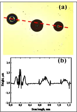
3.2 Micro-scale defects A large number of circle
dark spots ranging in size from hundreds of microns to millimeters were usually observed on the surface of films deposited at intermediate power (medium density) after oxidation in oxygen at a temperature in the range 550-650 oC.
Figure 4(a) shows a typical optical microscopy image of such spots. Optical profilometry showed that these spots are the projections (Fig. 4(b)) with a complex structure of the edge and the center. Usually these defects are formed around pin-holes or near the edges of the silicon substrate.
Figure 4 Optical microscopy image of the micro-defects (a) and
corresponding surface profile (b).
Pin-holes are formed due to micro-sparks on the sputtered target and these are the native defects in the thin films deposited by magnetron sputtering method.
IR spectra measured on defects and uniform surface using 50 µm x 50 µm aperture are almost identical (not presented here). However, micro-Raman spectra exhibit
intense signals of amorphous carbon in the dark spots (broad band in range 1000-1600 cm-1), while the signal is not detected on the surrounding surface (spectra not presented here).
Nano-probe Auger electron profiles of silicon, carbon and oxygen in the dark spot and in the open surface are shown in Fig. 5. It can be seen that in a homogeneous area of the film the distribution of the elements in depth of the film is homogeneous and corresponds to amorphous silica. In the dark spot the profile of the composition is represented by two areas: (1) the upper area with a high concentration of oxygen, and (2) the lower area, with high carbon content. The oxygen concentration drops at the boundary and then slowly decreases toward the silicon substrate. The silicon concentration in these two areas differs little. Thus we can conclude that dark spots are represented by a bi-layer: upper layer of silicon oxide and underlying nano-composite layer composed of amorphous silicon carbide and amorphous carbon precipitates.
Figure 5 AES depth profile of the distribution of silicon, carbon
and oxygen in the region of uniform surface (a) and “dark hole” defect (b).
When measuring the profile of the distribution of elements, the ion etching conditions were identical so the delayed arrival to a silicon substrate in the case of measurement over the dark spot is obviously due to the greater thickness in this location, which is consistent with optical profilometry data (see Fig. 4(b)).
(a)
(b)
0 200 400 600 800 0 500 1000 1500 2000 2500 3000 3500 0 500 1000 1500 2000 2500 3000Si substrate
(b)
Intensity, arb. un.
Etching time, s Si(LVV) C(KVV) O(KVV)
(a)
Si substrate
Summarizing the experimental data, we suggest a topological model of the dark defects as presented in Fig. 6. Significant increase of the thickness in the region of dark spot is probably associated with condensation of large amounts of carbon in the porous SiC matrix.
It is important to note that oxidation of the film – regardless of the film density,-leads to transformation of mechanical stress from compressive into tensile. As was shown in Section 3.1, oxidation of the amorphous SiC matrix results in shrinkage of the material, thus promoting relaxation of compressive stresses. The origin of such phenomena is probably associated with difference in the length of the silicon-carbon and silicon-oxygen interatomic bonds (0.19 nm and 0.16 nm, respectively) i.e. substitution of carbon by oxygen should result in “shrinkage” of the material. We suggest that such stress evolution serves as a driving force for carbon migration and precipitation during oxidation process.
Formation of the micro-defects around pin-holes or edge of the substrate is suggested to be a result of stress relaxation in these regions.
Figure 6 Topological model of the “dark hole” micro-defect.
4 Summary Amorphous carbon-rich SiC:H films
were deposited on silicon substrates by RF-magnetron sputtering of SiC target in argon/methane gas mixture. A series of films with different density was fabricated by varying the discharge power. The effect of low-temperature oxidation by dry oxygen on the formation of morphological defects was studied. It was shown that ini-tial stage of the oxidation of low density amorphous sili-con-carbon alloy thin films proceeds inhomogeneously in local nano-scale regions. Oxidation of amorphous SiC network is accompanied by (1) shrinkage of the material, resulting in transformation of mechanical stresses from compressive to tensile, and (2) release and migra-tion/diffusion of carbon species. Migramigra-tion/diffusion of carbon in combination with oxidation of SiC layer results in micro-scale morphological defects in the form of car-bon-enriched regions encapsulated between upper silicon oxide and bottom silicon substrate.
Acknowledgements This work has been supported by
Science and Technology Center of Ukraine, project No. 5513 and National Academy of Science project No. 2-2-15-28.
References
[1] X. Li, X. Wang, R. Bondokov, J. Morris, Yu. H. An, and T. S. Sudarshan, J. Biomed. Mater. Res. B 72, 353 (2005). [2] U. Schmid and H. Seidel, Sens. Actuators A 130–131, 194
(2006).
[3] J.-M. Hsu, P. Tathireddy, L. Rieth, A. R. Normann, and F. Solzbacher, Thin Solid Films 516, 34 (2007).
[4] C. Iliescu, B. Chena, D. P. Poenar, and Y. Y. Lee, Sens. Ac-tuators B 129, 404 (2008).
[5] G. Kotzara, M. Freasa, Ph. Abelb, A. Fleischmanc, Sh. Royc, C. Zormand, J. M. Morane, and J. Melzakd, Biomater. 23, 2737 (2002).
[6] A. V. Vasin, Sh. Muto, Yu. Ishikawa, A. V. Rusavsky, T. Kimura, V. S. Lysenko, and A. N. Nazarov, Thin Solid Films 519, 221 (2011).
[7] H. Wieder, M. Cardona, and R. Guarnieri, Phys. Status Solidi B 92, 99 (1979).
[8] J. Bullot and M. P. Schmidt, Phys. Status Solidi B 143, 345 (1987).