Ceramic Interposers for High Density Packaging in 3D LTCC
Technology
by
Arash ADIBI
THESIS PRESENTED TO ÉCOLE DE TECHNOLOGIE SUPÉRIEURE
IN PARTIAL FULFILMENT FOR A MASTER’S DEGREE
WITH THESIS IN ELECTRICAL ENGINEERING
M. Sc. A.
MONTREAL, Avril 22, 2020
ÉCOLE DE TECHNOLOGIE SUPÉRIEURE
UNIVERSITÉ DU QUÉBEC
It is forbidden to reproduce, save or share the content of this document either in whole or in parts. The reader who wishes to print or save this document on any media must first get the permission of the author.
BOARD OF EXAMINERS
THIS THESIS HAS BEEN EVALUATED BY THE FOLLOWING BOARD OF EXAMINERS
Mr. Ammar Kouki, Thesis Supervisor
Department of Electrical Engineering, École de Technologie Supérieure Mr. Dominic Deslandes, President of the Board of Examiners
Department of Electrical Engineering, École de Technologie Supérieure Mr. Yves Blaquière, Member of the Jury
Department of Electrical Engineering, École de Technologie Supérieure
THIS THESIS WAS PRESENTED AND DEFENDED
IN THE PRESENCE OF A BOARD OF EXAMINERS AND THE PUBLIC « March 19, 2020 »
ACKNOWLEDGEMENTS
I would like to emphasise my profound gratitude to the people who help, motivate and support me during past three years in order to achieve my purpose.
My sincere gratitude goes to my advisor Professor Ammar Kouki who support me through the whole program of master. In addition, he encourages me throughout my research project, gave me confident and knowledge to go further in this project and being a better researcher. In addition, I am grateful to the member of jury, Professor Dominic Deslandes and Professor Yves Blaquière for their feedbacks and comments.
Likewise, I would like to thank Normand Gravel, who was always ready to help and support for the fabrication process. Moreover, I would like to express my deep appreciation to my colleges at LACIME laboratory, Aref, Aria, Mohsen, Mostafa, Ali etc.
It is worthwhile to mention that this project was supported by Ferro Corporation, Ciena Corporation, McGill University and Mitacs.
The last and most important gratitude is for my parents and my sister who support me and encourage me throughout my whole life to reach my goals. With their absolute love and support, make my paths easier. Their love is a bridge between me and everything.
Les interposeurs en céramique pour des boîtiers optoélectroniques 3D à très haute densité d’intégration basés sur la technologie LTCC
Arash ADIBI
RÉSUMÉ
La croissance mondiale de l’utilisation des données s’accélère tous les jours. En raison de la technologie 5G utilisée dans les années qui arrivent et de l’Internet des objets (IoT), la demande pour plus de données à transmettre et plus de bande passante continuera à augmenter. Pour répondre à ce besoin et transfert cet énorme volume de données, les centres de données et les infrastructures de réseau nécessiteront une vitesse de transmission de données plus élevée dans une bande passante plus large. Afin d’arriver à cette vitesse élevée et à cause de la limite des systèmes opérant à des fréquence micro-ondes, l’utilisation hautes fréquences et des fréquences optiques est inévitable. Ainsi, l’émergence de la technologie SiP (System in Package) en photonique offrira une option viable pour répondre à cette demande technologique permettant aux nouvelles puces d’offrir une grande capacité de transmission sur une large bande passante. Afin d’intégrer ces dispositifs photoniques dans le même boîtier avec des composants électroniques, de nouvelles technologies rentables offrant une grande fiabilité et de très bonnes performances pour maintenir l’intégrité du signal sont nécessaire. Par ailleurs, ces technologies doivent faciliter la miniaturisation de boîtier électronique et optoélectronique. L’une des solutions pour réduire la taille du boîtier électronique et optoélectronique est d’utiliser une technologie multicouche telle que LTCC (Low Temperature Co-fired Ceramics), dans laquelle certaines parties du circuit sont intégrées aux couches internes. L’un des défis de ce type de structures est de connecter différentes couches à travers des trous et de permettre des assemblages multi-puces avec des interconnexion plus courtes que possible. Généralement, l’utilisation de TSV (Through Silicon Via) dans les substrats basés en silicium a été proposée comme l’une des technologies qui permet ce type d’intégration haute densité, malgré sa fonctionnalité limitée et un coût relativement élevé. Dans ce projet, nous proposons une nouvelle méthode pour les interposeurs verticaux dans la technologie LTCC. Cette méthode combine les avantages du LTCC telle que son coût de fabrication, une faible perte diélectrique aux ondes millimétriques et la possibilité d’intégrer des composants passifs et des lignes de transmission dans ses couches internes. Cela permettra de réaliser des courtes interconnexions et des trous de très haute densité.
La technique proposée est basée sur un nouveau procédé de fabrication de micro-trous qui est associé à l’ablation au laser avec des matériaux conducteurs personnalisés pour remplir des trous. Ainsi, cela permettra de réaliser des trous et des interconnexions de différentes dimensions dans le LTCC. Pour démontrer la faisabilité et la fonctionnalité de la technique proposée, diverses lignes de transmission sur différentes couches ont été conçues qui interconnectent des feuilles LTCC ultra-minces à travers des trous. Ces conceptions ont été simulées et optimisées avec l’outil de simulations HFSS dans l’objectif d’atteindre le taux de transmission de données le plus élevé dans une boîte miniaturisée. Le prototypage a été réalisé sur la feuille de céramique A6M la plus fine dans le marché par Ferro qui a 1 mil d’épaisseur.
VIII
Les trous de ces feuilles sont remplis par des conducteurs spécifique à base d’or conçu également par Ferro. Une étude expérimentale du diamètre réalisable des trous et la distance entre deux trous adjacents a été effectuée sur une feuille de 1-mil afin de montrer que l’intégration et l’interconnexion à très haute densité est possible.
Selon les résultats obtenus, la technologie LTCC ayant une fabrication plus facile pourrait être considérée comme une bonne alternative aux substrats de silicium pour les interconnexions passives. En outre, la TCV (Through Ceramic Via) pour les transitions verticales s’est avérée réalisable et offre une alternative viable au TSV avec un processus de fabrication plus simple et deux ou trois fois moins chère pour l’industrie. La fabrication du micro-via avec le diamètre minimum de 20 µm et la distance entre deux vias d’au moins de 40 µm est réalisable sur les feuilles de céramique avec l’épaisseur de 1 mil, tandis que le diamètre régulier du via est de 50 µm et la distance était de 200 µm, respectivement. En plus, l’épaisseur actuelle des feuilles de céramique dans l’industrie sont 10 mil, 5 mil et 2 mil (rarement utilisé). En utilisant cette feuille de céramique d’une épaisseur de 1 mil, la conception des circuits et les package RF plus dense et miniaturisé est plus réalisable.
Mots-clés : LTCC, Micro-Via, L’interposeurs céramique, optoélectronique, le boîtier
Ceramic Interposers for Ultra-High Density Packaging in 3D LTCC Technology
Arash ADIBI
ABSTRACT
The worldwide growth of data usage is continuing and accelerating. With the arrival of 5G technology and the Internet of Things (IoT), the demand for more data and more bandwidth will continue to rise. To support this enormous data volume flow, data centers and backhaul network infrastructure will require higher data transmission speeds with more bandwidth. To accommodate this trend, the use of optical frequencies is unavoidable due to the limitations of microwave-based systems. In this context, the emergence of photonic System in Package (SiP) technology offers one viable option to meeting these challenges offering chips that can provide high transmission capacity and support wider bandwidth. In order to integrate these photonic devices with the electronic components of a system in a single package, novel cost-effective packaging technologies that offer high reliability with very good performance to maintain signal integrity are needed. In addition, these technologies must allow for high density package for size reduction.
One of the solutions for decreasing the size of the package is the use of multi-layer technology, such as LTCC (Low Temperature Co-fired Ceramics), whereby parts of the circuit are integrated into the inner layers resulting in a multilayer functional package. One of the challenges in these kinds of structures is connecting different layers through vias and enabling multi-chip assemblies with very short interconnections. Traditionally, the use of Through Silicon Vias (TSV) has been proposed as one of the enabling technologies to allow for this kind of high-density integration, though with limited functionality and relatively high cost. In this thesis, a new method for the vertical interposers in LTCC technology is proposed. This method combines the advantages of LTCC, namely low-cost, low dielectric loss at millimeter wave frequencies and the ability to integrate passive components and transmission lines in its inner layers with those of TSVs for realizing very high-density short interconnects and vias.
The proposed technique relies on a novel micro-via fabrication process that combines laser ablation with custom conductor filling materials to realize various dimension vias and interconnects in LTCC. To demonstrate the feasibility and functionality of the proposed technique, various transmission lines on different layers interconnect through micro-vias and using ultra-thin LTCC green tape were first simulated and optimized using Ansys HFSS in order to reach the highest data transmission rate with smallest package possible. Prototyping was carried out using the thinnest Ferro’s A6M ceramic sheet with the thickness of 1 mil and filled the micro-via by custom engineered gold-based conductor paste, also provided by Ferro Corporation. However, the silver is a better conductor than gold in terms of conductivity, but the gold-based conductor paste has small grain size and low viscosity comparing to the silver-based conductive paste, which is more common to use. Thus, this customized conductive paste was chosen as conductor in this project since we have new size of via diameter in LTCC technology at this moment. An experimental investigation of the smallest via diameter and via
X
pitch that could be achieved using 1-mil thick sheets was also carried out and shows that moving towards reaching higher value of integration structure is possible. Then, this technique of micro-vias fabrication have been used in these two designed prototypes of an opto-electronic package hosing by LTCC for the collaboration project with Ciena Corporation and McGill university.
Based on the obtained results, LTCC technology with less fabrication complexity could be considered as a good alternative to silicon substrates for passive interconnects. Practical TCV (Through Ceramic Via) for vertical transitions have been demonstrated to be feasible and offer a viable alternative to TSV with simpler fabrication process and two- or three-times lower cost of manufacturing. The fabrication of the micro-via with the minimum diameter of 20 µm and the pitch size of at least 40 µm is achievable on the 1-mil ceramic sheets, while the regular diameter of via is 50 µm and the pitch was 200 µm, respectively. In addition, the current thickness of ceramic sheets for manufacturing are 10 mil, 5 mil and 2 mil (rarely used). By using this ceramic sheet with the thickness of 1 mil, designing the denser RF circuits and package is more feasible.
TABLE OF CONTENTS
Page
INTRODUCTION ... 21
CHAPTER 1 LITERATURE REVIEW ... 25
1.1 THROUGH SILICON VIA (TSV) ... 25
1.2 INTERPOSERS ... 27
1.3 MICRO-VIAS IN CERAMIC SUBSTRATE ... 31
1.4 3DSIP ... 34
1.5 LTCCTECHNOLOGY ... 35
1.5.1 ADVANTAGES OF LTCC ... 36
1.5.2 LTCCFABRICATION PROCESS ... 37
CHAPTER 2 LTCC FABRICATION PROCESS IMPROVEMENT FOR CERAMIC INTERPOSER REALIZATION ... 41
2.1 LTCCMICRO-VIA FABRICATION ... 41
2.1.1 MICRO-VIA FABRICATION STEPS ... 42
2.1.2 EXPERIMENTAL INVESTIGATION OF LTCCMICRO-VIA ... 43
2.2 TRANSMISSION LINE INTERCONNECTS ... 47
2.2.1 CO-PLANAR WAVEGUIDE ... 47
2.2.2 DIFFERENTIAL COPLANAR TRANSMISSION LINE ... 49
2.3 CERAMIC INTERPOSER INTEGRATION –SIMULATION ... 50
2.4 CERAMIC INTERPOSER INTEGRATION –FABRICATION ... 57
2.5 CONCLUSION ... 59
CHAPTER 3 OPTO-ELECTRONIC PACKAG DESIGN USING WIRE-BOND ... 61
3.1 OPTO-ELECTRONIC PACKAGE ON LTCC ... 61
3.2 FABRICATION OF OPTO-ELECTRONIC PACKAGE ... 66
3.3 CONCLUSION ... 68
CHAPTER 4 OPTO-ELECTRONIC PACKAGE USING FLIP CHIP ... 71
4.1 PACKAGE DESIGN WITH FLIP-CHIP DEVICES ... 71
4.2 SIPPROTOTYPE DESIGN AND FABRICATION ... 71
4.3 CONCLUSION ... 76
CONCLUSION ... 77
LIST OF TABLES
Page TABLE 1.1 DIFFERENT APPLICATION OF VERTICAL INTERPOSER ... 30 TABLE 1.2 USED CIRCULAR VIA DIAMETER IN DIFFERENT PROJECTS ... 33 TABLE 1.3 CHARACTERISTIC OF FERRO A6M CERAMIC TAPE AND CONDUCTOR PASTE ... 37 TABLE 2.1 COMPARING TWO CPW TRANSMISSION LINE AND VERTICAL INTERPOSER IN
SILICON AND CERAMIC SUBSTRATE ... 53 TABLE 2.2 COMPARISON BETWEEN THE SIMULATION AND MEASUREMENT RESULTS FROM
LIST OF FIGURES
Page FIGURE 1.1 LEFT:STRUCTURE OF TSV IN THE SILICON BACK-END INTERCONNECT STACK.
RIGHT:SEM OF FABRICATED TSV: ELECTRICAL DESIGN OF THROUGH
SILICON VIA ... 26
FIGURE 1.2 VIA ASPECT OF RATIO (DEPTH TO WIDTH) ... 32
FIGURE 1.3 LTCC FABRICATION PROCESS PROVIDED BY LACIME ... 39
FIGURE 2.1 VIA DIAMETER VS VIA PITCH ... 44
FIGURE 2.2 FABRICATED MICRO-VIA WITH VARYING VIA DIAMETER AND VIA PITCH ON 1-MIL THICK CERAMIC SHEET ... 44
FIGURE 2.3 3D IMAGE BY CONFOCAL MICROSCOPE.LEFT: SURFACE OF THE SHEET AND FILLED WITH 20 µM VIA.RIGHT:3D VIEW OF THE SAME MICRO-VIA ... 46
FIGURE 2.4 CROSS-SECTIONAL VIEW OF A CPWG TRANSMISSION LINE WITH ELECTRIC FIELD LINES ... 48
FIGURE 2.5 DIFFERENTIAL COPLANAR TRANSMISSION LINE IN THE FORM OF GSGSG. PHOTO TAKEN FROM (YIKUN YU,2010) ... 49
FIGURE 2.6 A TRANSMISSION LINE AND A ZOOM TO THE DESIGNED MICRO-VIA IN THIS STRUCTURE ... 51
FIGURE 2.7 SIMULATION RESULT OF S-PARAMETERS OF ONE-CHANNEL TRANSMISSION LINE ... 52
FIGURE 2.8 SCHEMATIC OF DESIGNED DIFFERENTIAL TRANSMISSION LINE IN FORM OF GSGSG WITH THE PITCH OF 125 µM BETWEEN THE LINES ... 54
FIGURE 2.9 THE NEAR-END (BLUE) AND FAR-END (RED)CROSSTALK SIMULATION RESULT OF DESIGNED TWO-CHANNEL TRANSMISSION LINE ... 54
FIGURE 2.10 SCHEMATIC OF DESIGNED TRANSITION FOR TWO CHANNELS ... 55
FIGURE 2.11 THE INSERTION LOSS (BLUE) AND THE RETURN LOSS (RED) OF SIMULATED TWO-CHANNEL TRANSMISSION LINE IN FIG.2.10 ... 56
XVI
FIGURE 2.12 THE NEAR-FIELD AND FAR-FIELD CROSSTALK RESULTS OF SIMULATED
TRANSMISSION LINE IN RED AND BLUE RESPECTIVELY ... 56
FIGURE 2.13 FABRICATION OF THE TRANSMISSION LINE USING MICRO-VIA ... 57
FIGURE 2.14 COMPARING SIMULATION RESULTS AND MEASUREMENT RESULTS ... 58
FIGURE 3.1 OPTO-ELECTRONIC PACKAGE ... 62
FIGURE 3.2 A TRIMETRIC VIEW OF THE OPTO-ELECTRONIC DESIGNED PACKAGE ... 63
FIGURE 3.3 CLOSE VIEW TO THE INTERCONNECTIONS OF PACKAGE THROUGH WIRE-BOND AND MICRO-VIA ... 63
FIGURE 3.4 THE CIRCUIT SCHEMATIC OF THE OPTO-ELECTRONICS PACKAGE ... 64
FIGURE 3.5 THE S-PARAMETER RESULTS OF THE CPW TRANSMISSION LINE USED IN THE PACKAGE ... 66
FIGURE 3.6 FABRICATED PACKAGE USING THE MICRO-VIA AND SMALL LINE-TO-LINE PITCH ... 67
FIGURE 3.7 X-RAY IMAGE OF FABRICATED MICRO-VIA INSIDE THE OPTO-ELECTRONIC SIP 68 FIGURE 4.1 AN ISOMETRIC VIEW OF THE ADVANCED OPTO-ELECTRONIC DESIGNED PACKAGE ... 72
FIGURE 4.2 A CLOSE VIEW TO THE DESIGNED INTERCONNECTION THROUGH MICRO-VIA .... 73
FIGURE 4.3 THE S-PARAMETER RESULTS OF THE CPW TRANSMISSION LINE USED IN 2ND ITERATION ... 73
FIGURE 4.4 LEFT:THE 3RD SAMPLE OF DESIGNED PACKAGE AND ITS MOLD AFTER FIRING. RIGHT:A CLOSE VIEW TO THE SAME FABRICATED PACKAGE AND THE CRACK BETWEEN CAVITIES. ... 75
LIST OF ABBREVIATIONS AND ACRONYMS
3D Three Dimensional 5G 5th Generation
ASIC Application Specific Integrated Circuit BEOL Back End Of Line
BER Bit Error Rate BGA Ball Grid Array
CMP Chemical Mechanical Polishing CPU Central Processing Unit
CPW Co-Planar Waveguide
CPWG Co-Planar Waveguide with Ground DC Direct Current
EM Electromagnetic
EMI Electromagnetic Interference FPGA Field Programmable Gate Array GCPW Grounded Co-Planar Waveguide GPU Graphics Processing Unit
GSG Ground Signal Ground
HFSS High Frequency Structure Simulator IoT Internet of Things
ISM Industrial, Scientific, Medical
LACIME Telecommunications and Microelectronics Integration Laboratory LCP Liquid Crystal Polymer
LTCC Low Temperature Co-fired Ceramic MaCE Metal-assisted Chemical Etching MEMS Micro Electro-Mechanical Systems MCM Multi-Chip Module
XVIII
RF Radio Frequency
RLCG Resistance, Inductance, Capacitance and Conductance SEM Scanning Electron Microscope
SET Single Electron Transistor SiP System in Package
SIW Substrate Integrated Waveguides TCV Through Ceramic Via
LIST OF SYMBOLS AND UNITS OF MEASUREMENTS
Ag Silver
Au Gold
°C Centigrade
Cu Copper
Gbps Giga bits per second mΩ/sq Milli-Ohm per square Pa.S Pascal Second
Ppm/°C Parts per million per centigrade Sq Square
W Tungsten
W/mK Watts per meter-Kelvin Ω Ohm
INTRODUCTION
Motivation and context
The worldwide growth in data usage is continuing and accelerating even more with the emerging of new technologies such as 5th generation (5G) of mobile networks, ultra-high-speed fiber for internet, TV broadcasting of 4K contents and sensor networks. Therefore, the demand for more data and more bandwidth will continue to rise. In addition, the development of communication systems and the number of accessible services on the devices operating at millimeter-wave frequencies, make it necessary to develop low-cost and high-density integrated circuits and packages while retaining their performance. To accommodate this trend, cost-effective multi-layer packaging technologies that offer high reliability with very good performance to maintain signal integrity are needed. These technologies must facilitate the size reduction for high-density packages. One of the main challenges in multi-layer structures is connecting different layers vertically through vias and enabling multi-chip assemblies with interconnections that are as short as and as dense as possible.
Problem statement
Traditionally, the use of vertical interposers on silicon-based substrates and Through Silicon Vias (TSVs) to interconnect different layers has been one of the enabling technologies to allow high-density multi-chip integration, albeit with limited functionality and relatively high cost of fabrication. TSVs are filled by conductors such as copper, tungsten or polycrystalline silicon and they must have an isolation layer enclosing the conductive material to electrically isolated the silicon substrate and the TSV. This thin isolation layer does not work appropriately at high frequencies (Jonghyun Cho, 2010) and will also increase the DC loss of the system. In fact, despite the promising performance of TSVs and silicon interposers at low frequencies, the low resistivity of the silicon substrate leads to an excessive attenuation of transmitted signal at higher frequencies and particularly at millimeter-wave frequencies. This high substrate loss
22
will become a significant barrier to having an acceptable RF performance and to the development of 3D System in Package (SiP) application based on silicon. Moreover, the high loss of signals in TSVs produces a high noise coupling coefficient among different signals of the system and therefore it could increase jitter, phase noise of clock signals and the bit-error-rate in the data transmission of RF systems (Helmy & Ismail, 2006). In addition, the integration of RF passive components in the inner layer of silicon multi-layer structure is challenging. This challenge makes the design more complex and increases the number of fabrication steps, which consequently increases the cost of manufacturing. Finally, one should also note that the costly part in the silicon interposer manufacturing is via fabrication, isolation and filling. Therefore, finding a technological solution that can provide similar integration capabilities of silicon interposers with TSVs while addressing its limitations is the key problem to be addressed in this thesis.
A LTCC technology-based interposer is one possible alternative to silicon interposers. Indeed, LTCC technology provides the possibility of having an arbitrary number of dielectric layers using very low loss materials with high conductivity metals such as silver (Ag) and gold (Au). It is a promising technology for the realization of 3D integrated circuits and is well suited for packaging. However, the achievable pitch, size of vias, line width and line-to-line spacing with conventional LTCC fabrication methods are not comparable to those that can be achieved with silicon interposers with TSVs. Therefore, for LTCC-based interposers to be viable, the problems related to the standard LTCC fabrication process must be addressed and solutions must be proposed and developed.
Thesis objectives
The main objective of this research project is to bring the necessary improvements to the LTCC fabrication process that will enable it to offer a viable and cost-effective alternative to silicon interposers with TSVs. The second objective is to apply the enhanced LTCC process to the design and realization of a small package for high-density SiP integration of an optoelectronic multi-chip module in collaboration with Ciena Corporation and McGill University. To reach
23
these objectives, we will seek to realize the smallest micro-via dimension that is possible to fabricate on the thin ceramic sheets along with narrowest transmission lines with the smallest possible pitch between vias as well as the lines.
Thesis organization
This thesis organized in four different chapters. The first chapter discusses the literature review regarding the vertical interposer on silicon substrate, TSV, micro-via, vertical interconnection on multilayer ceramic substrate and LTCC fabrication process. An experimental investigation of micro-vias in LTCC is presented in the second chapter. This chapter also presents a fabricated transmission line designed using the proposed micro-vias on a multilayer ceramic substrate. The third chapter introduces the design and fabrication of a first prototype for an opto-electronic SiP module using wire-bonds to connect the chips to the package. Afterward, a second prototype of this package, employing micro-vias and flip-chipped devices is presented in the fourth chapter. Finally, the last chapter provides a brief conclusion of the work accomplished.
Thesis contributions
The work presented here has led to the development of an enhanced LTCC process with demonstrated feasibility of through ceramic micro vias and small lines widths and pitches. The process makes the realization of ceramic interposers with through ceramic micro-vias feasible thereby offering a viable alternative to silicon interposers with TSVs. This process was utilized to realize a SiP package that was delivered to Ciena and McGill for the integration of a multichip optoelectronic module. The main results of this work were the subject of IEEE international 20th Electronics Packaging Technology Conference (EPTC) publication. In addition, I was participated on other paper which is under review to published on the journal of Transactions on Components, Packaging and Manufacturing Technology. Following are the details of these publications:
24
Adibi, A., et al., “Ceramic Interposer for Ultra-High Density Packaging and 3D Circuit Integration,” IEEE 20th Electronics Packaging Technology Conference, pp. 13-16, Dec 2018. Pourzadi, A., Adibi, A., Kouki, A., “A Fast Technique for Realization of Lumped-Element Values Into 3D Physical Layout on LTCC,” IEEE Journal of Transaction on Components, Packaging and Manufacturing Technology.
CHAPTER 1 LITERATURE REVIEW
In current telecommunication systems, due in part to the arrival of 5G technology and the Internet of Things (IoT), higher data speeds and greater bandwidth are required. The peak data rate for a whole system was around 100 Mbps in the late 1990s. By 2017 it had increased to more than 200 Gbps (C. Doerr, 2017). This need for higher speed of data transmission accelerates the need for new technologies and methods of data transfer to reach the desired rates and beyond. Therefore, this has served as a motivation for designers to move towards higher frequency bands such as millimeter-wave or optical frequencies (M. A. Jezzini, 2016). This increasing of the speed of transmission will increase the losses in microwave circuits and systems. On one hand, in millimeter-wave and optical frequencies, the physical length of components and circuits are much smaller compared to the wavelength. On the other hand, demand for low cost and high reliable technology maintain performance of the system, makes it inevitable to move towards a new technology of fabrication and 3D packaging. In this project, a cost-effective technical method for this purpose based on Low Temperature Co-fired Ceramic (LTCC) technology is proposed and demonstrated.
The first chapter of this thesis presents a literature review concerning the related subjects such as TSV, interposer, micro-via, multilayer SiP, LTCC presentation and its fabrication process.
1.1 Through Silicon Via (TSV)
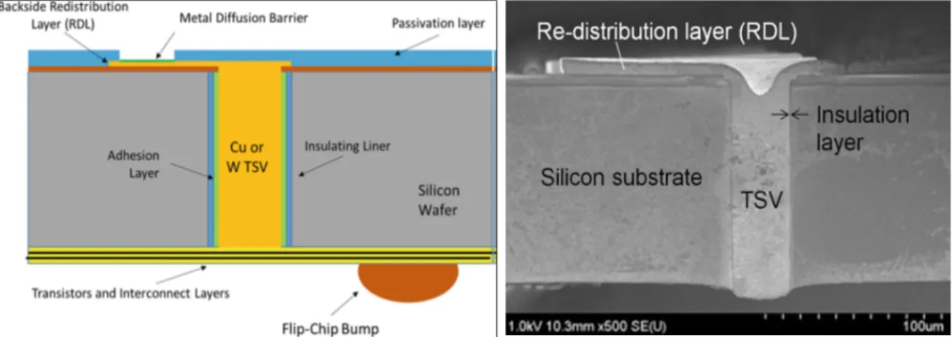
In multi-layer circuits or packages based on silicon substrates, TSVs (Through Silicon Vias) are used to create a vertical transition path for the signals between different layers. This technique is an alternative to connection through bonding wires in order to increase the number of I/O, decrease signal delay and therefore increasing the speed of data transmission. Figure 1.1 presents the structure of a TSV (left) with reference to the active device and back-end
26
interconnect stacking in a wafer (Ravi Mahajan, 2017), and a SEM (Scanning Electron Microscope) photograph of a typical fabricated TSV (right). These via-holes are isolated from the silicon substrate by a dielectric layer and then filled by conductor such as polycrystalline silicon, W (Tungsten) or Cu (Copper). It is important that these vias have the return and radiation losses as low as possible.
Figure 1.1 Left: Structure of TSV in the silicon back-end interconnect stack. Right: SEM of fabricated TSV: electrical design of through silicon via1
The silicon interposer has complicated fabrication process that increases the cost of manufacturing. In general, the costliest part is creating the hole via on the silicon substrate, isolation and filling. Fabricating this vertical electrical connection in a silicon substrate can be carried out by different techniques that require several steps. In one of these techniques, the first step is deep silicon etching where the holes are created on the silicon substrate. The next step is via oxide deposition to insulate the conductor from substrate to degrade the DC (Direct Current) loss of the substrate. After that, conductor plating is performed where a liquid conductor is injected into the hole. The processes of BEOL (Back End Of Line) Chemical Mechanical Polishing (CMP) or polishing the surface of wafer is the last step (Gong, 2014).
27
The silicon technology has some drawbacks at high frequency such as low resistivity for the TSV, ineffective isolation layer and high noise coupling coefficient among different signals due to the high value of signal loss. The resistivity of silicon substrate attenuates the signal passing vertically through TSV, and consequently this lossy signal degrades the RF performance at high frequencies (Soon Wee Ho, 2008). When current flows in the fine TSV, it can generate ohmic heat and accordingly hot spots in high-power chips, that negatively effect on the performance of the package (Heng Yun Zhang, 2014).
Additionally, the thin isolation layer surrounding the conductive material filled inside the TSV cannot prevent sufficiently the electrical parasitic coupling and critical substrate noise in the vicinity of active devices and/or adjacent TSVs. The effect of this noise is increasing the jitter and phase noise of clock signals as well as increasing the Bit-Error-Rate (BER) of the RF signals (Jonghyun Cho, 2010). In (Nauman H. Khan, 2011), coaxial TSVs with a diameter of 35.4 µm were used in order to overcome the noise issues of regular TSVs. In (Heng Yun Zhang, 2014), the TSVs with 10 µm diameter were used in high power circuits where two dummy dies and a thermal die were added to the circuit to improve the thermal performance of the structure.
1.2 Interposers
The word Interposer comes from a Latin origin “interpōnere” which means, “to put up between”1. An interposer electrically connects different parts of an electronic circuit through multiple layers and vias. In modern packaging technology, vertical interposers with flip chip attachments are used as an alternative to wire-bond connections. Generally, the performance of wire-bonds at frequencies above 30 GHz is not practical because it will have some impact on the performance of the device (C. Doerr, 2017). Due to the high characteristic impedance of wire-bonds, it would have an inductor behavior at high frequencies or behave as an antenna or a resonator (Rida, 2013). Therefore, wire bonding decreases the quality of the RF signals at
28
high frequencies. The interposers are employed as a good alternative for wire-bonds in 3D packages; and most interposers in use today are made with silicon substrates and TSVs. The use of silicon interposers is principally in the integration of Micro Electro Mechanical Systems (MEMS), Field Programmable Gate Array (FPGA) technologies, ASICs (Application Specific Integrated Circuits), server CPUs (Central Processing Unit), GPU (Graphics Processing Unit) and wireless devices (Timothy G. Lenihan, 2013).
In (Yan Yang, 2019), a CPW (Co-Planar Waveguide) transmission line on a silicon substrate in multilayer structure is presented where the Ground-Signal-Ground (GSG) TSV used for vertical interconnection. This structure operates in the frequency up to 40 GHz. The designed parameters of this transmission line such as via diameter, depth of via and center-to-center pitch of the lines are 20 µm, 100 µm and 100 µm, respectively. The (Kuili Ren, 2016) presents a development process of thick silicon interposer for integrated inductor, micro-strip and CPW transmission lines. In their paper, a TSV with the diameter of 80 µm and the thickness of 300 µm for vertical interposer is reported. In other work presented on (J-R. Tenailleau, 2013), a TSV developed for the RF interposer applications with the nominal diameter of 75 µm and pitch of 125 µm, which is scalable for industrial production. They tested this via on a structure of dual via chain including CPW transmission line access, which is operates in the frequency range of DC to 20 GHz. In (Liyi Li, 2015) a via with a diameter of 28 µm, a pitch size of 80 µm and a depth of 162 µm was fabricated on silicon substrate by using Metal-assisted Chemical Etching (MaCE).
At high frequencies, the ceramic interposer is a good alternative for the silicon interposer because of its lower resistivity and its easier fabrication process. In (Li & Zhou, 2015), a seven-stage cascaded coaxial impedance based on ceramic sheets of Ferro A6S designed to use as a vertical transition for low-pass structure in 20 layers. The reason of using these seven stepped coaxial impedances is increasing the bandwidth and decreasing the second order resonant frequency. This via transition works from DC up to 30 GHz and the diameter of via in this structure varies from 120 µm to 220 µm. The measurement results for the microstrip to
29
microstrip transition through the coaxial via from DC to 30 GHz were better than -12 dB and -0.5 dB for S11 and S21, respectively. Another work of vertical transition from microstrip to microstrip was reported in (Chih-Chun Tsai, 2011) where the via has a diameter of 135 µm and they achieved a return loss better than -20 dB and an insertion loss below than -0.48 dB for the whole ISM (Industrial, Scientific, Medical) band (DC to 67 GHz). In addition, the (T. Kangasvieril, 2006) reported three different transitions from GCPW (Grounded Co-Planar Waveguide) to GCPW, GCPW to microstrip and GCPW to stripline by employing the vias 150 µm in diameter in a 8-layer structure. The result of this work present good transmission characteristic up to V-band (50 GHz). The insertion loss and return loss measured -0.4 dB and -18 dB, respectively.
Table 1.1 summarizes the different research where the vias with varying diameter were used for different interposer applications.
30
Table 1.1 different application of vertical interposer
Via
diameter Thickness Frequency Application Substrate
Yan Yang, 2019 20 µm 100 µm DC to 40 GHz CPW transmission line Silicon Kuili Ren, 2016 40 µm 80 µm 70 µm 230 µm N/A Integrated inductor, micro-strip and CPW transmission lines Silicon J-R. Tenailleau, 2013 75 µm 200 µm Up to 20 GHz 2.5D Interposer applications Silicon
Liyi Li, 2015 28 µm 162 µm N/A Silicon interposer in
wafer level Silicon Li & Zhou, 2015 120 – 220 µm 2000 µm DC to 30 GHz Microstrip to microstrip transition
through Coaxial via
Ceramic Chih-Chun Tsai, 2011 135 µm 740 µm DC to 67 GHz Microstrip to microstrip Ceramic T. Kangasvieril, 2006 150 µm 800 µm DC to 50 GHz GCPW to GCPW GCPW to microstrip GCPW to stripline Ceramic
Clearly, as Table 1.1 shows, the main challenge for making ceramic interposers is the fabrication of smaller micro-via that can be comparable with the range of via diameter in silicon substrate.
31
1.3 Micro-vias in ceramic substrate
Micro-via is a crucial part of high-density interconnection in multi-layer SiP structures at high frequency, because it should support the small pitch between the pads of devices and between the adjacent lines. By increasing the frequency, the wavelength will be decreased. Consequently, the width of transmission line, the dimension of ICs and RF components that used in this range of frequency will also decreased. Therefore, creating the micro-via in order to make interconnection between different layers of package is crucial. In fact, fabricating the smallest possible via is the biggest challenge of multi-layer packaging. The value of via diameter and the small pitch between two adjacent vias can determine the miniaturization ability of the multi-layer packaging.
In conventional RF structures and circuits, the long interconnections and vias act as an undesirable transmission lines in high-speed data transmission, which causes an extra delay into the system. This transmission line behavior in interconnection happens when the electrical length of interconnection or via is longer than half of the signal rise time. Therefore, by increasing the frequency and the speed of signals, it will be important to keep these internal connections as short as possible. In addition, the short interconnections prevent having the high inductance in the system and thinner vias can reduce radiation loss; and consequently, the insertion loss is improved.
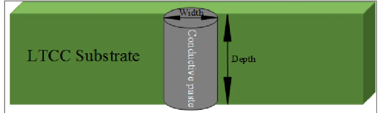
Furthermore, in order to achieve proper filling of micro-vias, the aspect ratio of the vias should be considered. The aspect ratio is the ratio between the depth (thickness of ceramic sheet) and width (diameter of hole) of vias as given by equation 1.1 and illustrated in figure 1.3. A via that has a smaller diameter than its length can be unrealizable for fabrication.
32
Indeed, the smaller the aspect ratio of vias is, the easier it is to fill it. The aspect ratio of via fabrication for mass production in industrial project is 0.64:1, which means that via diameter should be 64 percent of substrate height (IMST, 2011).
Figure 1.2 Via aspect of ratio (Depth to Width)
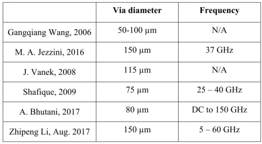
In (Gangqiang Wang, 2006), they achieved to drill and use the vias with the diameter between 50-100 µm in a six-layer high interconnect density design with a decent alignment. In (M. A. Jezzini, 2016), they used the vias with 150-µm diameter for multi-layer packaging on LTCC on the layers with the thickness of 127 µm and 254 µm. This design is working at the frequency of 37 GHz with 3 dB bandwidth. In paper (J. Vanek, 2008), an experimental test has been done to figure out the smallest via diameter realizable on different ceramic type of sheets. Hence, the smallest via diameter that built experimentally was 115 µm on the Ferro A6M tape with the thickness of 100 µm. In other works, a micro-via with 75 µm diameter on a 254 µm thick ceramic sheets was fabricated (Shafique, 2009) by using the 25 µm focal diameter laser for use in the fabrication of a Substrate Integrated Waveguides (SIW) operating at the frequency of 25 - 40 GHz. These resolutions were applied for substrate-integrated waveguide fabrication but remain far from the typical TSV resolution of 25 µm or better via diameter and a pitch of 50 µm or better.
In the SiP and multilayer package, the signal transition between different transmission lines has a key role in the structure. One of them is CPW to stripline signal transition and in (A. Bhutani, 2017) a fabricated via-based CPW to stripline signal transition is presented. This structure fabricates on the LTCC substrate tape of DuPontTM GreenTapeTM and operate from
33
DC to 150 GHz. In this broadband signal transition, they used signal via with the diameter of 80 µm for vertical transition. The shortest pitch of these vias was 200 µm and the thickness of layers was 106.7 µm after firing. In this design, an air cavity between signal via catch-pads and stripline, and circular apertures in lower ground of stripline employs in order to reduce the parasitic capacitance effect of structure. In (Zhipeng Li, Aug. 2017), a microstrip-to-microstrip signal transition is designed to operate from 5 GHz up to 60 GHz. In this structure two type of vias for signal and ground transition with different diameter are used. The diameter of signal via and ground via are 450 µm and 150 µm, respectively. In addition, in several project for millimeter-wave applications the researcher used the rectangular via for the vertical transition in multilayer structure. In (Isapour Aria, 2019), a vertical LTCC integrated waveguide for multilayer structure is presented, which is operates at the frequency around 60 GHz. The proposed structure facilitates the integration of passive component such as filters, couplers and power dividers perpendicular to the surface of structure. For this design, the rectangular vias were required to make the vertical waveguide.
Table 1.2 used circular via diameter in different projects
Via diameter Frequency
Gangqiang Wang, 2006 50-100 µm N/A M. A. Jezzini, 2016 150 µm 37 GHz
J. Vanek, 2008 115 µm N/A
Shafique, 2009 75 µm 25 – 40 GHz A. Bhutani, 2017 80 µm DC to 150 GHz Zhipeng Li, Aug. 2017 150 µm 5 – 60 GHz
The size of via is constrained between two boundaries. First diameter limit of micro-vias fabrication determined by the laser beams or punching machine, which limit the physical size during via drilling. Second, the viscosity of grain paste. This can limit the size of
micro-34
via where the viscosity decreases, the via diameter should increase and vice versa; otherwise, the conductive paste cannot fill the micro-vias properly. Based on the bibliography of previously published work regarding vias in ceramic substrate, which is summarized in table 1.2, the standard vias used currently on LTCC technology has the diameter varies from 50 µm to 150 µm with a pitch ranging from 150 µm to 300 µm. Via filling for these sizes is well established and is achieved with standard metal pastes.
1.4 3D SiP
The use of appropriate material and technology for millimeter wave and optical frequency packaging is important to have the optimum package size, impedance, and low loss. The 3D or multi-layer System in Package (SiP) technology is an advanced packaging method, which enables the designer to interconnect the integrated components and circuits in different layers together while also connecting them with the active devices located on the surface of the package. This is useful in applications such as: Single Electron Transistor (SET), FinFet Transistor, Integrated Circuit (IC) and etc. Current 3D technology for multi-layer low loss packaging is based on the silicon substrate and Liquid Crystal Polymers (LCP), (M. A. Jezzini, 2016). Due to their inconvenience for operating at the higher frequency, RF engineers have been motivated to use the ceramic substrate as an alternative to these technologies.
The development of this technology to operates at millimeter wave and optical frequencies with different functionalities requires that the devices be as small as possible, in addition to short and dense interconnections, smaller micro-vias and finer physical substrate. The reduction of the length of interconnections makes the propagation time shorter and decreases the parasitic effects. Additionally, the consumption and fabrication cost of the system decreases due to the reduction in the size of components, and the use of 3D packaging, (Rida, 2013). In the other hand, these dense multi-layer packages and their interconnections can increase the crosstalk between the channels.
35
In addition, substrate loss is a critical property in improving the functionality of 3D SiP. LTCC technology can provides the distinct opportunity for 3D packaging. It is one of the pioneer technologies that provide the possibility to integrate the passive components in the inner layers of structure and interconnect the integrated components to the other elements or transmission line on different layers or connect them to the active components where mounted on the surface of structure through the vertical interposer. While, the vertical interposers of silicon substrate and LCP substrate have their own constraint in optical frequency. The isolation layer of TSV works inappropriately at high frequency and LCP does not provide the necessary mechanical rigidity for vertical interposer (M. A. Jezzini, 2016). Furthermore, the cavity formation is another LTCC advantage in order to use for high-density package at high frequencies. LTCC technology facilitates the open or close cavity fabrication in any desire shape and depth. The main use of these cavities can be putting the component inside them in order to decrease their connection length.
The ability to integrate passive components inside of the LTCC substrate provide a package with high reliability by decreasing the number of interconnections and also reducing the length of them. The electrical elements that can be integrated in the inner layer of LTCC packaging technology including resistors, capacitors, inductors, LC shunts and series, the components such as filters and resonators, etc. Additionally, in this technology the value of capacitor and inductors can be easily increased by using respectively the conductive and magnetic tapes (Rida, 2013).
1.5 LTCC Technology
Low Temperature Co-fired Ceramic (LTCC) is a multi-layer technology used to design and fabricate passive components on 3D structure, which facilitates the size reduction of high-density and multi-functional RF package in millimeter-wave and optical frequencies. In this technology, the circuits and components designed with ceramic sheets use dielectric, resistive and conductive paste which are co-fired concurrently in an oven at the temperature below than 1000 °C (around 850 °C) for more than 12 hours. This sintering temperature enable the
36
designer to use the low resistance and high conductive conductors such as silver (Ag) and gold (Au) (Aria Isapour, 2017).
A conventional LTCC structure can include dielectric tapes, buried and surface-mounted conductors, transmission lines, passive components, resistors, interconnecting vias, surface-mounted electrical and optical devices. This technology has the possibility to design and fabricate the passive components in inner layers as buried components or on top layer as surface-mounted components. Therefore, LTCC is an assuring technology for 3D integrated structure and package that offer high reliability with very good performance. Generally, this technology is used in different applications such as passive components, integrated circuit, functional MCM (Multi-Chip Module) and System in Package (SiP).
1.5.1 Advantages of LTCC
LTCC technology has attracted the attention of RF designer because of its numerous advantages to operate at high frequency (up to 100 GHz). These advantages allow this technology to be a considerable alternative for current technology for 3D integration and fabrication of miniaturized package. In addition, it facilitates the integration of passive components in the inner layer of structure. LTCC has the following characteristics:
• Low loss conductor and tangent loss,
• Low dielectric loss at millimeter wave and optical frequencies, • Allow to use noble conductors such as silver (Ag) and gold (Au),
• Offers multilayer structure (up to 40 layers) with high accuracy of device alignment, • Possibility to integrate electrical passive component in inner layers,
• Better thermal resistance and thermal expansion coefficient than silicon substrate, • Better product reliability than silicon technology at millimeter wave,
• Compatibility with hermetic sealing, • Cost efficiency.
37
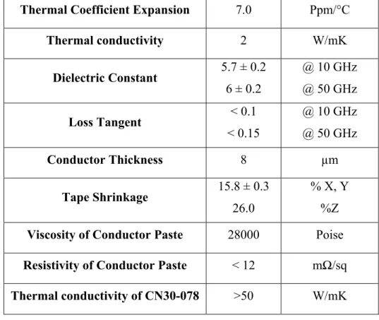
In this project, the A6M ceramic sheets provided by Ferro Corporation was used as a substrate with different thickness of 1-mil, 2-mil, 5-mil and 10-mil. The thinnest ceramic sheet (1-mil) has not yet be commercialized and is used only for research purpose. In addition, we used a customized gold-based conductive paste (CN30-078M) provided by Ferro for this tiny sheet. Table 2.1 present the typical properties of A6M ceramic tape.
Table 1.3 Characteristics of Ferro A6M ceramic tape and conductor paste1
Thermal Coefficient Expansion 7.0 Ppm/°C
Thermal conductivity 2 W/mK Dielectric Constant 5.7 ± 0.2 6 ± 0.2 @ 10 GHz @ 50 GHz Loss Tangent < 0.1 < 0.15 @ 10 GHz @ 50 GHz Conductor Thickness 8 µm Tape Shrinkage 15.8 ± 0.3 26.0 % X, Y %Z
Viscosity of Conductor Paste 28000 Poise
Resistivity of Conductor Paste < 12 mΩ/sq
Thermal conductivity of CN30-078 >50 W/mK
1.5.2 LTCC Fabrication process
The LTCC manufacturing process has various steps as shown briefly in figure 2.1 provided by LACIME (Telecommunications and Microelectronics Integration Laboratory), laboratory at
1 Technical Data Sheet of Ferro A6M/A6M-E High Frequency LTCC Tape System and A6M/A6ME LTCC Au
38
ETS (École de Technologie Supérieure). The fabrication process is simplified and demonstrated different phase of LTCC manufacturing procedure as an infographic.
The LTCC fabrication process begins with cutting green tapes with the dimension of 12x12 cm. This dimension is the acceptable dimension of fabrication devices that used in LACIME laboratory. Then, the sheets are punched by laser machine or punching machine in order to make the vias. The difference between these machines is that laser machine offer drilling the vias in different shapes and diameter size, whereas the punch machine has some predefined vias with different size. In the laboratory of LACIME, we have the opportunity to use the punching machine and the LPKF U3 laser machine with a minimum diameter of 15 µm to make micro-vias. Generally, the punching machine is used for making the vias with regular diameter sizes in the ceramic sheets; and similarly, to create the alignment via in the corners of the tape. The alignment via is several standard vias in two different sizes of 3 mm and 150 µm that located in the four corners of the sheet in order to facilitate the precise alignment during the fabrication process. On the other side, the laser machine has the ability to use for making any circular or rectangular via with different diameter sizes (LTCC Process Design Rules, 2018). Although milling with a laser beam diameter of 15 µm allows to drill vias smaller than 50 µm in LTCC, the coarse metal grain in standard metallic pastes makes via filling of such micro-vias impossible.
39
Figure 1.3 LTCC fabrication process provided by LACIME1
Afterward, the drilled vias will be verified by microscope to investigate if their shapes are correct and drilled properly. Then, the vias are fill by appropriate conductive paste manually or by printing machine. The next step is conductor printing where the conductor lines are print on the surface of every needed sheets. As an additional process of this step, the ablation will be done on the conductor lines in order to trim them or create the necessary dimension and shapes on them. Subsequently, these individual sheets are collated and stacked by a stack machine; after that the structure is put in the isostatic press machine in order to completely remove any undesired tiny space of air between the layers. After the laminating steps, the LTCC structure with the dimension of 12x12 cm is cuts to one or several structures with suitable dimensions. Finally, these structures are co-fire on the oven at the temperature of around 850 °C for more than 12 hours. Post treatments on the structure can be done if the conductors must be trimmed. The last step is mounting the surface-mount devices and wire-bond them to the ceramic structure.
40
One of the benefits of this kind of multi-layer fabrication process is that each layer is fabricated separately, and it could be replaced or re-fabricated before stacking if any damages or defects is found on the sheets. This advantage of fabrication process compared with the silicon technology will save the time because it prevents re-manufacturing the whole structure, and therefore keeps the cost efficiency of fabrication.
CHAPTER 2
LTCC FABRICATION PROCESS IMPROVEMENT FOR CERAMIC INTERPOSER REALIZATION
To offer a viable option to silicon interposers, TSV’s diameter, pitch to pitch of vias and width of lines in silicon substrate, we must be able to achieve very small vias (micro-via) with the diameter in the range of below 50 µm (the current minimum via diameter in LTCC technology) and as close as possible to the range of 20 µm, single ended and differential transmission lines with line widths and pitch of 100 µm and 125 µm, respectively. In this chapter, we investigate the feasibility of ceramic interposers and propose the necessary LTCC process improvements that will help meet the goal.
Following the LTCC technology and fabrication presentation, an experimental investigation regarding the realizable small micro-via diameter and small center-to-center via pitch will be introduced. This investigation was carried out on a thinnest Ferro’s A6M ceramic sheet with the thickness of 1-mil which is available currently for the research purpose. Afterwards, in order to demonstrate the functionality of the proposed technique of micro-via fabrication for high frequency circuitry, these thin ceramic sheets and fabricated micro-vias were experimentally used to build the 50 Ω CPW (Co-Planar Waveguide) transmission lines. These transmission lines have been designed as a multilayer structure using Trough Ceramic Via (TCV) to connect the surface printed lines with the buried lines located in inner layer.
2.1 LTCC Micro-Via Fabrication
This section is focused on the realization of micro-vias in LTCC technology as an alternative to TSVs.
42
2.1.1 Micro-via Fabrication Steps
Realizing a micro-via in LTCC fabrication process consists of two important steps: first steps is punching or drilling the via holes in the ceramic sheets and the second ones is filling them with an appropriate conductive paste. In this process, every step has its limit in order to manufacture vias and decreasing their diameter size. In general, there are two issues that limit the diameter size of micro-via; the first one is laser beam diameter, and the second one is the viscosity and particle size of the conductive paste for filling the vias. While the laser process determines the minimum feasible via pitch before the two adjacent vias mechanically collapse, the viscosity and grain size of the conductive paste limits the size of the minimum via diameter that can be filled properly.
In this project, an LPKF U3 laser machine with a laser beam of 15 µm diameter is used to drill the micro-vias. Then, the via filling is carried out on a thick film screen-printing machine with adjustable vacuum under tapes for proper filling. This vacuum facilitates the leaking of conductive paste into the hole. In fact, the viscosity of the paste, using for via filling has the reverse relation to the vacuum using in this process. Similarly, with the same conductive paste, if the diameter of vias are small, then the vacuum should be more intense than using the via with larger diameter size. Furthermore, the grain size of conductive paste is also an important factor of manufacturing; since the pastes with the bigger grain size are unable to enter and fill the holes that has smaller outer diameter size. Therefore, to be able to realize smaller micro-vias, a paste with small grain size along with a thin LTCC green tape are needed. To this end, a customized custom gold-base conductive paste (Au8886-A) provided by Ferro Corporation was used.
In order to overcome the second limit of micro-via fabrication and filling the holes properly by this customized conductive paste, which has low viscosity, the aspect ratio of micro-via should be as small as possible. Therefore, a custom 1-mil thick Ferro green tape was used in this project. It is worthwhile to mention that the 1-mil thick Ferro’s ceramic sheet was not available for commercial purposes yet.
43
2.1.2 Experimental Investigation of LTCC Micro-Via
To determine the best realizable micro-via diameter and minimum possible pitch, an experimental investigation was performed by using the thinnest Ferro’s A6M ceramic sheet and special conductive gold-based paste fabricated by Ferro Corporation. First, an array of vias with varying diameter size and different pitches was created. In this investigation, the micro-via diameters ranged from 16 to 36 µm in the steps of 2 µm. The reason of choosing the size of 16 µm as the smallest via diameter is the limit of LPFK U3 laser machine, which has a laser beam of 15 µm. In addition, the center-to-center pitch of vias was varied from 26 µm for the smallest diameter (16 µm) to more than 100 µm for the larger micro-vias in the steps of 5 µm. The figure 2.1 in below presents a diagram of the designed micro-via’s array in different diameter and pitch combinations to be fabricated. In general, the minimum pitch of micro-vias for every diameter have been chosen to start from via diameter size plus 10 µm; for example, the minimum pitch of 18 µm via diameter is 28 µm and the minimum pitch for the diameter of 36 µm is 46 µm. The designed array of micro-via was fabricated on a 1-mil thick LTCC green tape and the figure 2.2 shows a photograph of seven most interesting columns of these filled micro-vias. In this picture, each column represents vias of the same diameter with increasing spacing between them going down.
44
Figure 2.1 Via diameter vs Via pitch
Figure 2.2 Fabricated micro-via with varying via diameter and via pitch on 1-mil thick ceramic sheet
45
The result of this experimental investigation was examined by a 3D confocal laser microscope, Olympus LEXT OLS 4000, available at LACIME laboratory. In order to determine the smallest realizable via diameter, we consider the last row of micro-vias where the spacing between adjacent vias is largest.
Based on this examination, the vias with the diameter of 16 µm and 18 µm had unacceptable circular shape. Because the laser machine with the laser beam of 15 µm was unable to properly drill this range of diameter size; and accordingly, the filling of these series of micro-vias were impractical. On the other side, for the micro-vias with the diameter of 30 µm and beyond, there were lack of metallization. The reason is that this conductive paste was incapable to fill appropriately these ranges of micro-vias with big aspect ratio. In fact, this gold-based paste has the small grain size and low viscosity (15-25 Pa.s1 at 25.5 °C ± 0.5 °C) comparing to the regular conductive past. Therefore, during filling the micro-via even without using the vacuum option from bottom of the ceramic sheet, the conductive paste spread out from the other side of the holes with large size of via diameter.
Unlike these two ranges of via diameters on the corners of the designed array, the micro-vias with the diameter between 20 – 28 µm were drilled correctly in a circular shape with accurate diameter size. In addition, they filled properly by the customized conductive gold-based paste. Consequently, to take advantage of this 1-mil thick ceramic sheet, we were limited to use the micro-vias with the diameter between 20 – 28 µm.
In addition to the smallest via diameter, the minimum possible center-to-center pitch of micro-via should be determined. Thus, in order to determine the smallest pitch, the column of the micro-via with the diameter of 20 µm considered as the smallest filled micro-vias and again a visual inspection with the 3D confocal microscope has been done. Therefore, the 40 µm of center-to-center pitch was detected as a smallest pitch of two adjacent filled micro-vias. In general, based
46
on our experimental investigation and validated with fabrication, the pitch of micro-via should be at least twice of the diameter of the micro-vias.
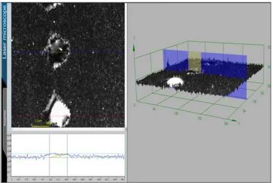
Figure 2.3 demonstrates a picture of two adjacent micro-vias with the diameter of 20 µm and the center-to-center pitch of 40 µm. This picture was taken by 3D confocal microscope where a pair of micro-vias was drilled correctly and filled appropriately.
Figure 2.3 3D image by confocal microscope. Left: surface of the sheet and filled with 20 µm via. Right: 3D view of the same micro-via
As the consequences of this experimental investigation, the 20 µm micro-via is considered as a smallest realizable diameter size for manufacturing the micro-vias on this thin ceramic sheet and the 40 µm treated as a minimum center-to-center pitch of via that is feasible to fabricate in this range of micro-via.
This experimental investigation was verified by visual inspection through 3D microscope in order to verify the conductive paste filling inside the micro-via, alongside the verifying short connection between adjacent vias. Furthermore, we used an ohmmeter to check the electrical
47
connection the micro-vias. At the end, we wrote a design rules for the micro-via fabrication including the dimension of the via, convenable conductive paste, how to inject the conductive paste to the via, required vacuum below the ceramic sheets during filling the micro-via, etc.
2.2 Transmission Line Interconnects
In general, transmission line is a conductor trace that conduct the signal of radio frequency from a source or emitter to the receiver or load. It consists of two conductors for the signal and its return path. LTCC technology can support all kind of transmission line, but we focused on the single ended and differential transmission line in the form of CPW (Co-Planar Waveguide).
2.2.1 Co-Planar Waveguide
In this project, we use the CPW transmission line to connect the electrical and optical components of the package. CPW is a planar transmission line that consists of three conductors, which support signal transition on the same plane. It includes one single conducting track in the center, and two return path conductors located at the two sides of the conducting track with an equal gap. The CPWG (Co-Planar Waveguide with Ground) is a common variant of the CPW line, whereas a ground plane located on the other side of the dielectric substrate as a third return conductors. This ground plane is connected to two other return paths on top of the dielectric trough the vias in order to reduce losses.
In printed circuit board technologies, CPW transmission lines are made on top of the dielectric substrate, in this case ceramic substrate. Furthermore, the CPW line is vertical symmetrical from the middle of central line. The characteristic impedance (Z0) of this transmission line is determined by the physical gap between the central line and two sides return path, along with the width of the conducting line, whiles the thickness of dielectric has no impact on the impedance of CPW. This advantage of CPW and CPWG line comparing to the microstrip and stripline facilitate the signal transitions from narrow transmission line to wider ones and wise versa without requiring any changes on the thickness of dielectric substrate. This possibility
48
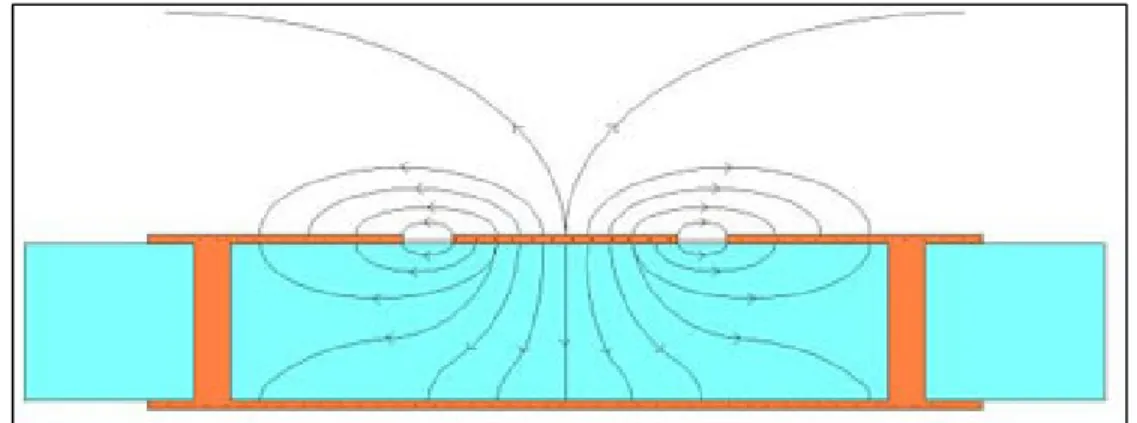
will be useful to connect the devices with different pad sizes and pitch of pads in a package. In addition, CPW transmission line can be used as a surface printed line and buried line in multilayer structures. All the transmission lines used in this work were CPWG. Figure 2.4 shows a CPWG transmission line with its electric fields.
Figure 2.4 Cross-sectional view of a CPWG transmission line with electric field lines1 The CPW line have some advantage comparing to the other type of transmission lines such as high isolation between signal traces, because there is a ground line between them. In addition, the CPW transmission line has less loss comparing to the microstrip line specially at higher impedance, which make it a better choice for compact layout. Also, it has less dispersion than microstrip for the millimeter wave frequencies. Contrariwise, CPW transmission line has two more track than microstrip, so it takes more space and it has lower heat transfer possibility comparing to microstrip.
Based on the symmetrical characteristic of the CPW, it can support four mode of excitation. These modes are including coplanar mode, slot-line mode, parallel plate mode and microstrip mode. The coplanar mode of excitation in CPW is not purely TEM, it is more quasi-TEM because the conductors are in contact with two different material which is substrate and air. Also, the parallel plate mode excited while the top and bottom ground of CPW are connected through the vias by the distance inferior than λg/10.
49
2.2.2 Differential Coplanar Transmission Line
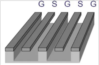
The differential transmission line is a structure of information transmitting consist of two symmetric conductive signal paths for the inverting and non-inverting signal in addition to a single ground path, whereas these two balanced signals flow in opposite-phase currents but with equal amplitude. Normally, the total impedance of differential transmission line is twice of the impedance of each line when they conduct individually. As the advantage of differential transmission lines, it can reduce emitted electromagnetic radiation, minimizes electronic crosstalk, less EMI (Electromagnetic Interference) and better noise protection. The higher resistance to the interference source facilitates using the differential signaling for longer distance between the transmitter and receiver of the system. Contrariwise, the disadvantage of this technique is that the differential signals are always accompanied by a some common-mode signal due to the unbalanced amplitude. Figure 2.5 shows a differential CPW transmission line in the form of GSGSG (G and S stands for Ground and signal respectively).
Figure 2.5 Differential coplanar transmission line in the form of GSGSG. Taken from Yikun Yu, (2010)
Due to the advantages of differential transmission line in high-speed digital circuits and high data rate transmitting systems, it is more commonly used in modern designs. Comparing to the single-ended transmission line, the differential transmission line is more immune to keep the difference voltage between the driver and receiver, and it is also protected against having the
50
common noise couples into the both terminations. Also, differential transmission line has the possibility to transit the signals twice faster than single-ended transmission line, whiles it consumes lower voltage.
Regarding the noise effect on differential transmission line, the noise affects equally on the positive and negative sides of the signals; in the other hand these two sides of differential transmission lines are separated by a physical gap into different paths. In addition, the differential signaling considered the potential difference between the two lines of differential transmission line and therefore the effect of noise on these two paths of system canceled each other. Consequently, the transmitting system with differential transmission line is more robust to the noise comparing to the single-ended transmission line.
In order to have a good differential transmission line, it should have uniform cross section, symmetry in the width and spacing of the lines. Moreover, the lines length must be equal to have the same time delay in both transmitting lines.
2.3 Ceramic Interposer Integration – Simulation
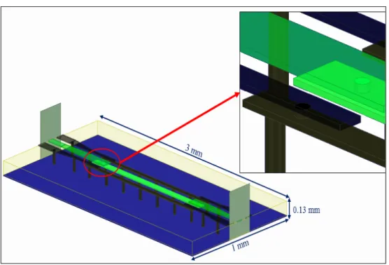
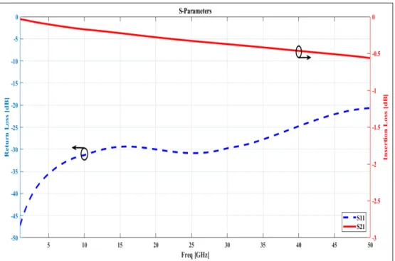
In this part, the designed transmission lines for one channel and then for two channels in multi-layer structures are presented and showed in the figures 2.6 and figure 2.8, respectively. In each design, a single micro-via was used for every line to connect the top layer to the below layer. These simulated structures that are presented below has three layers consist of two 1-mil sheets and one 5-mil sheet below them. This structure with only three layers is so fragile, therefore, we added some extra sheets under these layers in order to support the structure physically without any electrical effect on the transmission lines behavior. In this work, the transmission lines designed with different pitch of lines from 125 µm to 252 µm. In these two designs, the minimum spacing between the lines was 60.5 µm and 160 µm respectively for the pitch of 125 µm and 252 µm. In order to achieve these small spacing, we used the ablation technique during post processing of fabrication process.
51
At the first simulation with the pitch of 125 µm, the single channel CPW transmission line designed to be a 50 Ω, both at top layer and inner layer. This transmission line, figure 2.6, has the characteristic such as center conductor width of 68 µm, a ground lines of 61 µm and micro-via diameter of 24 µm.
Figure 2.6 A transmission line and a zoom to the designed micro-via in this structure The results of this simulation confirm that the insertion loss of the designed single transmission line is above -0.6 dB and the return loss is inferior than -20 dB for the entire simulated frequency band from 1 to 50 GHz. The S-parameter results of this one-channel 50 Ω CPW transmission line presented in the figure 2.7.
52
Figure 2.7 Simulation result of S-parameters of one-channel transmission line
In a similar project based on silicon substrate which was presented in state of the art, (Yan Yang, 2019), they have obtained the simulation results of > -0.35 dB and < -15 dB for insertion loss and return loss, respectively. Table 2.1 compare the CPW transmission line on silicon substrate presented on (Yan Yang, 2019) and the CPW transmission line on ceramic substrate presented in this work. This comparison confirms the similar results for the simulation of the CPW transmission lines on the silicon substrate and on the ceramic substrate.
53
Table 2.1 Comparing two CPW transmission line and vertical interposer in silicon and ceramic substrate
Yan Yang, 2019 This work
Substrate Silicon Ceramic
Via Diameter 20 µm 24 µm
Substrate Thickness 100 µm 130 µm
Center to Center Pitch 100 µm 125 µm
Insertion Loss > -0.35 dB > -0.6 dB
Return Loss < -15 dB < -20 dB
Frequency Up to 40 GHz Up to 50 GHz
After that, we added another channel alongside the first conducting line with the common ground line between these two channels in order to have a transmission line in the form of GSGSG. This two-channel interconnection presented in figure 2.8, was designed to have two adjacent 50 Ω CPW lines with a pitch of 250 µm between the centers conductors of two channels while the line width, the gap between the lines and micro-via diameter are the same as the one-channel transmission line designed.
Figure 2.9 shows the simulated results of near-end and far-end cross talk for this two-channels structure in blue and red, respectively. The presented figure demonstrates that the value of the two crosstalk was below than -30 dB for the entire frequency band from 1 to 50 GHz.
54
Figure 2.8 Schematic of designed differential transmission line in form of GSGSG with the pitch of 125 µm between the lines
Figure 2.9 The near-end (blue) and far-end (red) Crosstalk simulation result of designed two-channel transmission line