To cite this version :
Msolli, Sabeur and Baazaoui, Ahlem
and Alexis, Joël
and Kim,
Heung Soo Identification of damage and fracture modes in power
electronic packaging from experimental micro-shear tests and finite
element modeling (2018) Engineering Fracture Mechanics, vol. 188.
pp. 470-492. ISSN 0013-7944
O
pen
A
rchive
T
OULOUSE
A
rchive
O
uverte (
OATAO
)
OATAO is an open access repository that collects the work of some Toulouse researchers
and makes it freely available over the web where possible.
This is an author’s version published in :
http://oatao.univ-toulouse.fr/18652
Official URL :
https://dx.doi.org/10.1016/j.engfracmech.2017.09.014
Any correspondence concerning this service should be sent to the repository administrator :
[email protected]
Identification of damage and fracture modes in power electronic
packaging from experimental micro-shear tests and finite
element modeling
S. Msolli
a, A. Baazaoui
b, J. Alexis
b, H.S. Kim
a,⇑aDepartment of Mechanical, Robotics and Energy Engineering, Dongguk University-Seoul, 30 Pildong-ro 1-gil, Jung-gu, Seoul 100-715, Republic of Korea b
Université de Toulouse, INP/ENIT, LGP, 47, Avenue d’Azereix, F-65013 Tarbes, France
Keywords: Micro-shear CZM model GTN model Bifurcation theory
Finite element method (FEM)
a b s t r a c t
Micro-shear tests are performed in order to characterize the mechanical behavior and the fracture of the chip/metallized ceramic substrate assemblies of power electronic devices. These assemblies are elaborated using three types of junctions: AuGe solder/Au or Ag finish, transient liquid phase bonding (TLPB) AgIn/Ag finish and Ag nanoparticles/Au or Ag finish. The experiments are associated to finite element simulations of both nano-indentation and micro-shear tests. The mechanical behavior of the different assembly interfaces is repre-sented using an in-built cohesive zone model (CZM) available in the user friendly finite ele-ment code Abaqus!
. It is worth noting that the fracture mechanisms observed during the test and service periods of the power electronic packaging are not only due to the debond-ing at the interfaces but also to the initiation and growth of voids in the joint. Therefore, in addition to the CZM model, Gurson-Tvergaard-Needlmann (GTN) damage model is used in combination with the Rice bifurcation theory to correctly describe the fracture in the joint and, therefore the overall fracture mechanism of the entire junction. The simulation results are compared with the experimental force displacement curves and the SEM observations in order to assess the implemented model.
1. Introduction
One of the challenges in high temperature power electronics is the reliability of the chip/substrate in the packaging assembly. This concerns not only the quality of the die attachment but also the thermomechanical stability of the thin or thick metallizations plated either on the chip or on the copper double bonded ceramic substrate (DBC) surfaces. Experimental studies on power electronics assemblies presented in previous frameworks have shown cohesive and inter-facial ruptures within the junctions (solder, Ag nanoparticles, . . .), the Cu substrate and the diamond chip[1–3]. At high loading rates, the damage originates close to the interfaces due to the formation of fragile intermetallic compounds, the presence of defects at the interfaces or the weak adhesion of certain layers of surface finishing metallization [4,5]. However, fracture mainly remains in the bulk solder at slow strain rates. In order to optimize the design of high-temperature packaging, in particular with regard to their lifetime, it is no longer sufficient to know the mechanical behavior of the constitutive materials. Indeed, interfaces and junctions are privileged zones of initiation and propagation
⇑Corresponding author.
of cracks in packaging; it is, therefore, important to be able to describe this overall mechanism using finite element mod-eling tools. The interfaces are mainly represented by cohesive laws which make it possible to evaluate the initiation and the evolution of the interfacial damage by linking the effort at the interface to its opening distance. However, the param-eters of these laws are not exploitable from standard characterization tests and specific tests must then be implemented. The behavior laws of cohesive elements are usually described in terms of traction versus separation, which relates the interface relative displacement to the traction vector. Generally, the cohesive elements behave elastically until damage ini-tiation and obey a softening behavior afterwards. The specific energy dissipated by the cohesive element can be calculated from the area under the curve. Different constitutive laws of the cohesive zone model have been proposed in the literature
[6–11]. Since the shape of the function may influence the results of the simulation[12,13], it is crucial to identify a law that is suitable for capturing the interfacial fracture extension behavior of the cohesive layers. According to the nature of the material (ductile, brittle, etc.) and the type of loading considered (monotonic or cyclic loadings), the cohesive zone model can be defined. The bilinear cohesive zone model is currently the most widely used model for interfacial fracture behavior simulation due to its ability to describe different fracture modes and its availability in ABAQUS!
software. Thus, it has been widely used to characterize the interfacial damage behavior in power electronic packaging[14,15]. These studies showed the performance of the bilinear cohesive zone methods for describing and predicting crack initiation and propagation at the interfaces of electronic assemblies. They also demonstrated the convergence between the numerical simulation and experimental results.
Damage can also be observed in the solder joints. Damage is mainly present in the form of micro-voids. These voids grow and nucleate during the service period leading to cracking and failure. To describe this phenomenon and for lifetime predic-tion, many studies have focused on continuum damage theories or fatigue criteria to describe degradation in solders. These models are mainly coupled to plasticity or viscoplasticity constitutive equations to describe the plastic deformation prior to damage initiation[16,17]. For example, some fatigue criteria such as Darveaux[18]or Manson-Coffin[19]are usually used because they are practical in numerical frameworks and give correct predictions. They can predict the lifetime of real prod-ucts with complex geometry. However, the models take into account only the initial and final states of the material. The practical procedure to identify material behavior using these fatigue models is usually geometry dependent. In the general framework of continuum thermodynamics of irreversible processes, micro mechanical and phenomenological damage models are widely used[20,21]. These models are built from complex constitutive equations that require advanced integra-tion methods. Another approach for describing fracture in solders is the maximum entropy fracture model. This type of
Notations
Mathematical operators and symbols ð_xÞ x derivative with respect to time (xij) second order tensor x (i and j)
x: x = xijxij contracted product of two second order tensors xij
x # x = xijxkl tensorial product of two second order tensors xij
Variables and parameters
Ce elastic stiffness tensor (MPa)
D; Dp macroscopic strain and plastic strain rate tensors E,
v
Young modulus (MPa), Poisson ratiof ; f0; fc; fF total, initial, critical, final volume fraction of voids
fN; sN;
e
N nucleation material parametersGc fracture energy of the cohesive element (MPa.mm) K hardening coefficient (MPa)
Kh cohesive element stiffness (MPa.mm$1)
n power exponent
n normal to the Gurson yield surface (tensor) n
!0 vector normal to the localization band
q1; q2; q3Gurson model parameters
ti; t0i dual stress vector of the cohesive element, maximum value of stress (MPa)
di relative displacement of the cohesive element in direction i (mm)
d0i; dif relative displacement at damage initiation and complete failure (mm) dmaxi maximum relative displacement reached during loading (mm) dij second order unit tensor
e
0 yield strain of the matrix#
r
; #e
p effective stress (MPa) and plastic strain of the matrixmodel permits life predictions for a structure in the presence of microstructural uncertainty using the maximum entropy principle [22]. Among the interesting features in the model, a single damage parameter is used for the crack initiation and propagation in solder joints. Some interesting frameworks have used cohesive zone fracture mechanics and the Dis-turbed State Concept to predict the crack trajectory and fatigue life of solder interconnections subjected to both isothermal temperature cycling and anisothermal temperature cycling conditions[23]. The method correlates very well with the exper-imentally observed damage. A number of other studies dealt with the evolution of the damage within the void volume frac-tion[24–26]. They consider damage as an internal variable which particularly depends on the stress triaxiality. Voids effects are also taken into account using the specific yield function proposed by Gurson[27]or Tvergaard-Needlman[28]which introduces the volume fraction of voids in the dissipation or viscoplastic potentials[29]. A major framework consists on describing voids nucleation and growth of creeping solids using a particular formulation of the Cocks creep law. The model is successfully applied for the case of cyclic shear of tin based solders[16,17].
The main aim of the current paper is to conciliate the interfaces and joint damage in a finite element modeling. We intro-duce the development of a tool to describe the damage behavior of both interfaces and joints of power electronics assemblies based on experimental observations. The applications are concerned with the elaboration of electronic components by AuGe soldering, transient liquid phase bonding of Ag-In, or the sintering of Ag nanoparticles. This tool is based on the combination of simple shear tests coupled with an inverse method of parametric identification.
In this contribution, we first describe the experimental procedure and the results from the shear and nano-indentation experiments. These experiments will serve as verification and validation of the finite element framework. In the second sec-tion, a finite element modeling of the performed nano-indentation and shear tests is carried out. A bilinear cohesive zone model (CZM) and GTN damage model are selected for the interfaces failure and for the description of damage behavior of the joint, respectively. Since strain localization occurs prior to the initiation of cracks in the joint, the Rice bifurcation theory is adopted. The most interesting features of this approach are its physically based character and its ability to detect the occurrence of necking instabilities under complex loading conditions. Accordingly, we selected this approach for use in the prediction of the moment of strain localization in electronic junctions. The coupled bifurcation theory and GTN model are implemented in the finite element code Abaqus/explicit!
as user subroutine VUMAT. The models are calibrated and val-idated using the previously obtained experimental results.
2. Experimental characterization 2.1. Elaboration of the shear assemblies
Shear assemblies are manufactured using different techniques. These assemblies are constituted of Ni/Au or Ag metallized Oxygen/Halogen Free Copper (OHFC) inserts of dimensions 3 mm ' 3 mm ' 2 mm which are bonded on Ni/Au or Ag metal-lized OHFC copper substrates of dimensions 30 mm ' 20 mm ' 2 mm using different joining techniques: AuGe soldering with both Ni/Au and Ag metallization on the substrates, transient liquid phase bonding (TLPB) using Ag-In with both In pre-form and In metallization and, sintering of Ag nanoparticles (melting temperature Tm= 961 #C) with both Au and Ag finish
metallization on the substrates. The thickness of Ni and Au metallization is 4 mm and 3 mm respectively. The thicknesses of the Ag metallization used to elaborate the AuGe, Ag-In and Ag nanoparticles junctions are 50 mm, 4 mm and 4 mm, respec-tively.Table 1 summarizes the metallization and thickness for each type of assembly. The gold germanium solder is a 88Au12Ge eutectic alloy with a melting temperature of 356 #C. The TLPB technique is based on the diffusion of In into Ag met-allization after reflow and annealing of In. The expected Ag-In junction is a solid phase eutectic of which the melting tem-perature is up to 695 #C. This eutectic is composed of 33 wt% of In. The overall thickness of the junctions (including metallizations) is about 100 mm. A cross-section of the assemblies is presented to study the chemical composition of the junctions.
Microstructural observations using SEM and physico-chemical analyses of junctions formed by AuGe soldering on an Au finish or an Ag finish were carried out on the metallographic cross-sections. For the AuGe junction on an Au finish, these anal-yses show the formation of a continuous joint, free from defects. No noticeable porosity is observed either at the interfaces or in the joint, as demonstrated inFig. 1(a). The microstructure of the joint differs depending on whether it is located near the
Table 1
Metallization thickness of the inserts and substrates used to elaborate the shear assemblies. Metallization thickness (mm) Joint Ni Au Ag AuGe 4 3 50 Ag nanoparticles – 3 4 Ag-In – – 4
insert or the substrate. The difference is due to a variable cooling rate in the joint during the solidification taking into account the difference in the size of the insert with respect to the substrate. At the AuGe/Cu insert interface, a gold-rich phase is observed. In the AuGe/Cu substrate interface, a eutectic structure is observed with the presence of the two phases, an Au-rich phase and another Ge-Au-rich (Fig. 1(b)).Fig. 1(c) shows the chemical composition of the junction along the thickness. The evaluation of the chemical composition at the interface illustrated first, the formation of a porous layer due to the dif-fusion of phosphorus in the NiP layer and secondly, the difdif-fusion of Ge in the Ni barrier layer to a depth of about 1 mm. Thus, the 3
l
m thick gold finish layer deposited on the nickel was dissolved during soldering. Therefore, taking into account the NiGe phase diagram, an intermetallic type NiGe with a mass composition of 50 wt% of Ni and 50 wt% of Ge was formed in the AuGe/Cu insert and AuGe/Cu substrate interfaces. This is in agreement with the results by Hornberger et al., concerning this type of junction[30]. The NiGe intermetallic compound can weaken the solder joints by reducing their resistance to shear and can be a factor in breaking the interfaces. The migration of Ge to Ni metallizations leads to a decrease of its proportion in the AuGe layer. This phenomenon can lead to the destruction of the eutectic structure.For the bond formed by AuGe soldering on an Ag finish, the joints formed are continuous and of high quality, as illustrated inFig. 2(a). The morphology of these joints is homogeneous, symmetrical and presents no defects. The Energy-dispersive X-ray spectroscopy (EDX) analysis inFig. 2(b) shows the presence of a gold-rich phase at the two interfaces of the AuGe/Cu insert and AuGe/Cu substrate. In the center of the bond, a regular eutectic structure is observed with the presence of two phases: a Au-rich phase and a Ge-rich phase. The evaluation of the chemical composition and the micrographic analysis show the presence of a 5
l
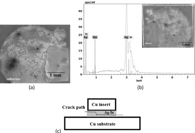
m thick interdiffusion zone between the Ag metallization and the AuGe solder at both AuGe/Cu inter-faces. This new AuGeAg ternary alloy which constitutes an interphase between the Ag layer and AuGe has a melting temper-ature of 500 #C, higher than that of AuGe which is in the order of 360 #C[30]. In the case of this junction, no intermetallic layer is observed at the interfaces.Fig. 3(a) shows the microstructural analyses carried out from metallographic cross-sections of the Ag-In junction obtained with indium metallization. The micrographs show the formation of a continuous joint with the presence of a few porosities in the center of the bond. The presence of the porosities in the joint is the result of the reflow operation; the porosities can be induced in particular by the initially rough structure of the indium. Thus, the evaluation of the chem-ical composition from an EDX profile reveals that the joint is composed of a maximum of about 20 wt% of indium at the center of the bond (Fig. 3(c)).
Microstructural analyses of the Ag-In bond carried out with In preform show the formation of a more porous bond than that produced with In metallization (Fig. 3(b)). These porosities are caused by the rough and porous structure of the In solder before reflow. The EDX analysis of the cross-section profile is almost the same as that observed previously for the Ag-In junc-tion made with In deposited metallizajunc-tion. The maximum In composijunc-tion of the juncjunc-tion is about 20 wt% at the center of the junction. This composition tends to decrease toward the interfaces with the insert or substrate (Fig. 3(d)).
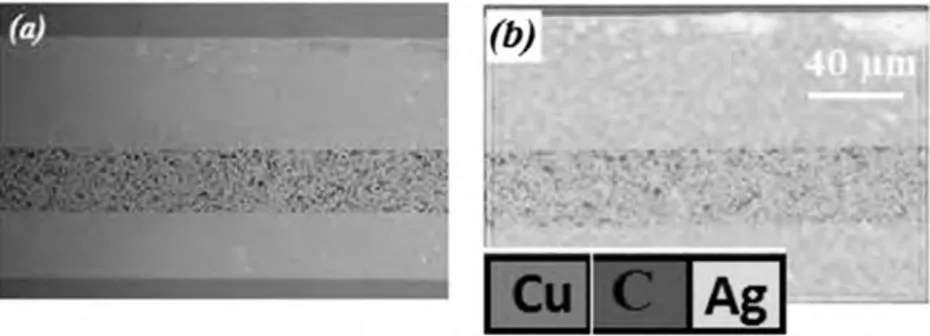
Physicochemical observations were made and analyses were carried out of the bond formed by sintering of the Ag nanoparticles. As illustrated inFig. 4(a), the micrographic analysis shows the formation of a continuous, homogeneous, and uniform joint without macroscopic defects. In the microstructure of the junction, a high porosity ratio is observed among the Ag grains which are smaller than 10
l
m in size. EDX mapping shows the presence of carbon compounds spread over the entire joint (Fig. 4(b)).2.2. Shear experiments
Displacement rate-controlled shear tests with a constant velocity of 1 mm/min are carried out at room temperature on elaborated shear test assemblies. The loading corresponds to an estimated strain rate of 0.16/s. The implementation of these experiments is performed in order to highlight the predominant shear behavior observed during the elaboration process and thermal cycling. Therefore, it is expected that these experiments activate the same physical phenomena. The choice of the experiment and the measured quantities are very important and the obtained results must be carefully monitored. The experiments are carried out using an INSTRON tensile machine dedicated to performing shear tests on electronic devices.
Fig. 1. (a) Micrograph of the cross-section of the AuGe/Au junction. (b) EDX mapping of the junction showing thicknesses and elements present. (c) Chemical composition of the junction against thickness.
The load cell of the tensile machine can handle forces up to 2 kN. The samples are fixed on the machine tray, while the punch that must push the insert is driven at a constant displacement. Meanwhile, an innovative non-contact detecting system using the digital images correlation technique (DIC) was introduced to measure the displacement of the assembly. This tech-nique is an optical method of non-contact measurement of two-dimensional (2D) kinematic fields. The image correlation measurement system consists of a Charge Coupled Device (CCD) and an optical system. The system is able to measure the surface displacements of an object with a displacement resolution of 5 mm. A schematic diagram of the experimental device is shown inFig. 5. The method of fine shear displacement measurement involves tracking markers between the sheared stud and a substrate reference element. The non-contact measuring system makes it possible to record the displace-ment between the two markers A and B located on the upper flat surface of the sheared part and the upper flat surface of a
Fig. 2. (a) Micrograph of the cross-section of the AuGe/Ag junction. (b) EDX mapping of the junction showing thicknesses and elements present. (c) Chemical composition of the junction against thickness.
Fig. 3. Micrograph of the cross-section of the Ag-In junction performed with (a) In metallization and (b) In preform. Chemical composition of the junction against thickness. (c) In metallization and (d) In preform.
reference stud, respectively. It should be noted that the dark color reference markers inFig. 5represent points A and B to measure the displacement of the assembly.
The reference pad is placed so that points A and B are in the focal plane of the sensor. Therefore, the measurement is insensitive to the parasitic displacement induced by the various elements of the machine and the measurement corresponds to the real shear displacement of the evaluated stud. The results will therefore be used to extract the load-displacement responses of the assembly and to calibrate the parameters of the interfaces and the junction models.
Fig. 6shows the force displacement curves recorded by the INSTRON tensile machine. InFig. 6(a), the results of displace-ment obtained from the force-displacedisplace-ment curves for the different cases of assemblies correspond to the accumulation of displacements specific to the joints, the interfaces, and the displacement induced by the mounting rigidity. Since the mount-ing system is extremely stiff compared to the remainmount-ing constitutive materials of the tested assembly, the force displace-ment responses are quasi-linear. The effect of the mounting rigidity is also deduced by stackable responses at the earliest stage of loading. Nevertheless, it can observed that the assemblies elaborated with the AuGe solder and Ag metallization are clearly the strongest. The junctions based on silver nanoparticles are not resistant compared to the other studied junc-tions. This is due to the nature of this type of junction, which is extremely porous at the gross state and after the thermo-mechanical process. The initial void density in these junctions is very high leading to weakening of the obtained bond. A fast drop of the reaction force is observed for all types of junctions. This indicates that immediately before this brittle failure, the crack propagates least on the assembly interfaces.Fig. 6(b) shows the force displacement curves with the experimental shear displacements measured using the DIC technique for the two types of junctions i.e. AuGe/Au and nano Ag/Ag. Actually, the
Fig. 4. (a) Micrograph of the cross-section of the Ag nanoparticles junction. (b) EDX mapping of the junction showing thicknesses and present elements.
Fig. 5. Schematic representation of the principle of the performed shear test.
Fig. 6. Force displacement curves of shear tests (V = 1 mm/min and T = 25 #C) for Cu-Cu assemblies. (a) Machine tray displacement. (b) Real shear displacement.
nonlinear behavior of the force displacement response can be observed, demonstrating that plasticity occurred in this assem-bly before cracking. This observation is based on the fact that copper and AuGe alloy exhibit plastic deformation before frac-ture. However, this is different for the Ag nanoparticles/Ag junction where the overall response is linear. Since Ag is a highly ductile material, the cracking is interpreted as an early debonding of the brittle and weak assembly interfaces.
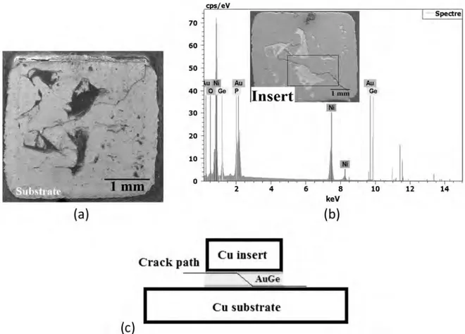
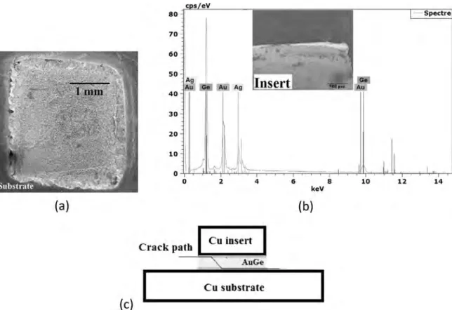
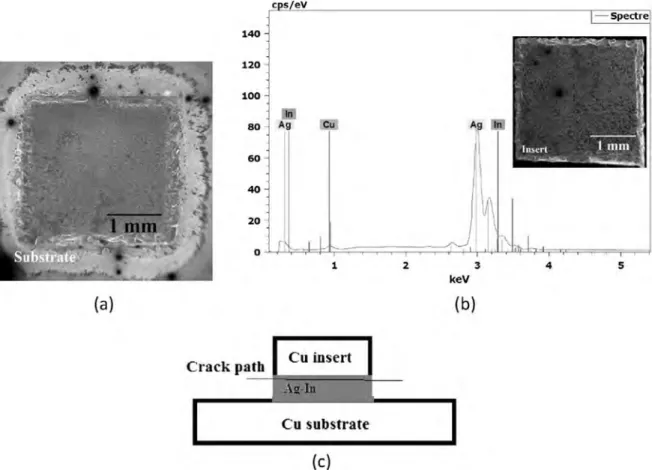
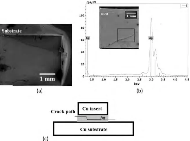
The shear tests are followed by the fractographic analysis of the various junctions. This analysis makes it possible to locate the fracture areas and thus to analyze the damage modes in order to identify the fracture path. The micrograph (Fig. 7(a)) and the EDX analysis of the fracture faces of AuGe specimens on Au finish reveals two distinct zones of different sizes: a Ni-rich area and smaller Au and Ge-rich areas (Fig. 7(b)). These analyses show that the failure first occurred in the AuGe/deposited Ni interface at the Cu substrate side, then propagated in the joint to reach the AuGe/deposited Ni interface at the Cu insert side. Therefore, one can deduce that the rupture is mixed: mainly adhesive at the interfaces between the Ni deposit and the AuGe solder, but also cohesive in the AuGe solder (Fig. 7(c)). In the case of the AuGe junctions on the Ag finish, the micrographic analysis (Fig. 8(a)) and the chemical composition show a substantially cohesive failure in the joint, close to the Cu insert. Indeed, according toFig. 8(b), the EDX analysis shows high proportions of Au and Ge. However, Ag-rich areas are also present on the fracture faces of this junction. The rupture of the AuGe junction is therefore mixed: cohesive in the solder and adhesive at the AuGe/Ag deposit interface of the Cu insert (Fig. 8(c)). No trace of Cu is present on the faces of the two types of junctions. Analysis of the fracture faces of the Ag-In TLPB specimens showed a cohesive fracture in the joint in the case of assemblies with In metallization (Fig. 9(a)) and a mixed rupture in the case of assemblies with In preform (Fig. 11(a)). The fracture is cohesive in the AuGe solder and adhesive in the Ag-In/Ag deposit interface at the insert side. Evaluations of the chemical com-position and the EDX analysis performed on the fracture faces reveal the exclusive presence of Ag and In after rupture in both types of assembly (Figs. 9(b) and11(b)). The evaluation of the fracture faces of the Ag-In assembly with In metallization using 3D optical profilometer showed that rupture occurred at 62
l
m with respect to the surface of the Cu substrate while the total joint has an initial thickness of about 100l
m before loading (Fig. 10).The EDX analyses of the fracture faces of the Ag nanoparticle sintering specimens show the exclusive presence of Ag (Fig. 12(b)). The micrograph analysis (Fig. 12(a)) and evaluation of the chemical compositions of the Ag nanoparticle assem-blies illustrate a mixed mode of failure. The rupture is cohesive in the Ag nanoparticles joint and adhesive at the Ag nanopar-ticles/Ag deposit interface of the Cu insert (Fig. 12(c)). From these various tests, it is concluded that the mechanical strength of the AuGe assembly is better on the Ag deposit. This can be explained in two ways: the solder forms an interphase com-posed of an Au-Ag solid solution at the AuGe/Ag deposit interface. This is possible because the two constituents Au and Ag, are perfectly miscible. Nevertheless, a seemingly fragile AuNiGe compound is formed at the interface between the solder and the Ni deposit because the thin Au deposit dissolves during the reflow of AuGe. The better mechanical strength of the Ag-In junction with the deposited Ag-In compared to that with the Ag-In preform can be explained by the better metallurgical quality of the Ag-In junction performed by deposition which is void-free. Finally, the junction with the Ag nanoparticles has a limited mechanical strength considering the porous structure of the bond. It should be noted that the shear strength of 28 MPa that was obtained with the Ag deposit corresponds to the maximum mechanical strength of 30 MPa recommended by the sup-plier (NBETech).
2.3. Nano-indentation experiments
Additional nano-indentation tests were performed at room temperature on the cross-section of the shear assemblies. Specifically, 15 idents were made in the AuGe and Ag nanoparticles layers. The tip used for the test is a Berkovich indenter with a Dynamic Contact Module (DCM) to determine the force displacement response of the joint materials. The nano-indentation test includes a unique loading unloading cycle with a maximum imposed displacement of the tip of 1 mm. The loading unloading curves are illustrated inFig. 13. Different behaviors are recorded for the two tested materials. The AuGe alloy exhibits more hardening than the Ag nanoparticles as the load reached is 3 times higher than that of Ag. 3. Finite element modeling
The performed nano-indentation and the shear tests are simulated using the finite element code Abaqus/Explicit. The experimental data such as force displacement responses are employed to calibrate the material parameters of the CZM and GTN models. More specifically, the nano-indentation tests are retained as reference results to determine the parameters of the Swift law. Subsequently, the damage parameters including those of the GTN and CZM models are obtained using shear tests with a fixed insert dimension of 3 mm ' 3 mm. Finally, in order to evaluate the robustness of the entire set of model parameters, a finite element simulation of a validation shear test is performed using a different geometry configuration for the assembly.
3.1. Nano-indentation test
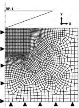
Finite element simulation of a 2-D axisymmetric nano-indentation model was performed as illustrated inFig. 14. The model consists of a rigid conical indenter that moves toward an elastoplastic substrate. A loading and unloading cycle is applied in this model. The indenter reaches a maximal displacement of 1 mm and is then retrieved. The substrate was meshed
with 6874 four-node bilinear axisymmetric quadrilateral, reduced integration elements as shown inFig. 14. For more pre-cision in stress distribution, a fine mesh was used under the contact area and in the vicinity of the tip. However, the mesh is coarser everywhere else to reduce the computational time. The simulations are performed using Abaqus/explicit solver with a nonlinear geometry option. As noted previously, the substrate shows an elastoplastic behavior that obeys the Swift law. No damage is considered in these simulations. The substrate has an ‘‘infinite” thickness (100 mm) compared to the imposed tip displacement.
3.2. Shear test
A simplified finite elements simulation of the tested assembly is performed under the FE code Abaqus. The aim of these computations is to simulate the crack initiation and propagation in the assembly. The fractography results for both the AuGe solder and the Ag nanoparticles based assemblies discussed in Section1, showed a brittle damage in the Cu/solder interfaces. To predict the interfacial and brittle damage behavior observed experimentally, the irreversible and bilinear cohesive zone model[14,15]can be applied. The 2D configuration of the assembly or the elementary packaging shown inFig. 15is com-posed of an OHFC copper insert and an OHFC copper substrate that are bonded together with the different junctions described previously, as well as two cohesive layers and a rigid shear tool. The two cohesive zone layers are placed in the junction/insert and junction/substrate interfaces, where fracture is typically observed. The whole part is subjected to shear within a displacement controlled loading. The imposed tool velocity is 0.2 mm/s for a total time of 1 s. These conditions lead to a maximal insert displacement of 0.2 mm since fracture is initiated at a maximum of 0.15 mm displacement. Thus, the simulations are quasi-static. For the copper insert and substrate, an elastoplastic model with isotropic hardening is adopted
[31]. For the behavior of the junctions, Swift plastic law is retained. Indeed, most of the commonly used solders exhibit vis-coplastic behavior since the temperature of the power electronic assembly is high compared to the melting temperature of the solder. This is the case for many alloys such as tin, lead or leadfree solders that have a melting temperature close to the application temperature. In the present case, the choice of elastoplastic modeling of the junctions is motivated by the fact that the targeted new packaging assemblies were initially designed and tested for temperatures up to 125 #C. This temper-ature represents about one-third of the melting tempertemper-ature of the AuGe solder alloy (Tm: 365 #C). This temperature is also
Fig. 7. Analysis of fracture faces of the Cu-Cu assemblies in the case of the AuGe junction on (b, c) Au finish. (a) SEM micrograph of the substrate fracture faces. (b) EDX chemical composition of the insert fracture faces. (c) Schematic of the crack path in the shear assembly.
very low compared to the melting temperature of silver nanoparticles (Tm: 800 #C). In the case of extreme temperature, the
model needs to be extended to the case of viscoplasticity. A complete description of the viscoplastic modeling of the tin sol-der behavior using unified Chaboche constitutive equations and using the Chaboche-type model combined with the Cocks’s damage law for porous creep can be found in[16,17], respectively. The models have previously been implemented in the FE code Abaqus. The Chaboche-type model is especially interesting as it can capture commonly observed features such as kine-matic hardening as well as voids nucleation and growth in the solders under cyclic shear. It proposes a modified viscoplastic potential based on the Cocks creep law which can be a convenient alternative to incorporating damage in the modeling framework.
Since the main mechanism of initiation and propagation of cracks in the junction is due to the nucleation and growth of voids, this law is then coupled to the GTN damage model to describe degradation in the solder. To determine the moment of strain localization in the junction, a bifurcation approach is used based on the calculation of the preferred orientation of the sliding plane. The thickness of the cohesive and joint layers, measured experimentally, is about 4 and 5 mm, respectively. The two cohesive layers were modeled using a 4-nodes bilinear quadrilateral element of type 2D cohesive (COH2D4). The length of the cohesive elements was 100 mm. In the thickness, the cohesive zone must be discretized with a single layer of cohesive elements[8]. In this case, the path of the cracking is naturally determined by the overall field and the cohesive response. The junction, the insert and the substrate layers were meshed with a 4-node bilinear 2D plane strain quadrilateral elements (CPE4R). The size of the elements in the solder is the same as that of the cohesive elements.
3.3. CZM model
For pure-mode I and pure-mode II or mode III loading, the available traction separation law (TSL) assumes the linear elas-tic behavior followed by the initiation and evolution of damage. A high initial stiffness is used to hold together the top and bottom faces of the debonding element in the linear elastic range. Once the peak values of the normal or shear nominal stress have been reached, the stiffnesses are gradually reduced to zero. The analytical expression of the bilinear cohesive model law relating the traction or the dual stress vector t to the interface’s relative displacement vector d is expressed as follows
[12,32]:
Fig. 8. Analysis of fracture faces of the Cu-Cu assemblies in the case of the AuGe junction on Ag finish. (a) SEM micrograph of the substrate fracture faces. (b) EDX chemical composition of the insert fracture faces. (c) Schematic of the crack path in the shear assembly.
ti¼ Khdi if di6d0i ð1 $ DiÞKhdi if d0i < di< dif 0 if diPdif 8 > > < > > : i ¼ 1; 3 ð1Þ Di¼ dif d max i $ d 0 i % & dmaxi d f i $ d 0 i ' ( ð2Þ
Fig. 9. Analysis of the fracture faces of the Cu-Cu assemblies performed using Ag-In TLPB with In metallization. (a) SEM micrograph of the substrate fracture faces. (b) EDX chemical composition of the insert fracture faces. (c) Schematic of the crack path in the shear assembly.
where d0 i and d
f
i represent the relative displacement at damage initiation and complete failure, respectively. d max
i refers to the
maximum value of the relative displacement attained during the loading history. Khis the cohesive element stiffness. d0i and
dif are given by Alfano[12]:
d0i ¼ t0 i Kh and df i ¼ 2Gc t0 i ð3Þ
Gcrepresents the fracture energy of the cohesive elements. A fundamental aspect in the formulation of the cohesive model is the requirement that the energy dissipated at a fracture propagation must be equal to the fracture energy, so that the fol-lowing relation (Eq.(3)) must be satisfied:
Gi¼
Z dif 0
tiddi¼ Gc ð4Þ
In this paper, only the pure-mode II debonding problem is considered, so that the analysis is simplified by focusing on scalar interface relationships relating one relative-displacement component d to t. In this case, the CZM characteristic param-eters are the cohesive element stiffness Khwhich is related to the cohesive layer modulus Ec, the fracture energy Gcand the
strength t0.Fig. 16illustrates the different variables of the CZM model in the case of a pure-mode II debonding problem.
3.4. GTN model
The original version of the Gurson model[27]was extended by Tvergaard and Needleman[28]and the latter version is referred to as the Gurson, Tvergaard, and Needleman (GTN) model. The GTN model considers ductile failure as a repercussion of nucleation and growth as well as the coalescence of spherical voids. The expression of the yield function is given as follows:
U
GTN¼ q #r
' (2 þ 2 q1f*cosh 3 q2R
m 2 #r
* + $ 1 $ q3f*2¼ 0; ð5ÞFig. 11. Analysis of the fracture faces of the Cu-Cu assemblies performed using Ag-In TLPB with In preform. (a) SEM micrograph of the substrate fracture faces. (b) EDX chemical composition of the insert fracture faces. (c) Schematic of the crack path in the shear assembly.
R is the macroscopic stress vector. The effective stress q and the pressure stressRmare equal to
ffiffiffiffiffiffiffiffiffiffiffiffiffiffiffiffiffiffiffi 3R:R=2 p
and trðRÞ=3, respectively, #
r
is the flow stress of the fully dense matrix, and f*is the modified volume fraction of voids. q1, q2and q3are material constants and take the values of 1.5, 1 and 2.25, respectively[33].
f*is introduced in order to improve the description of the coalescence stage. Its expression is given by the empirical
for-mula introduced by Tvergaard and Needleman[28]:
Fig. 12. Analysis of failure faces of the Cu-Cu assemblies performed using sintering of Ag nanoparticles. (a) SEM micrograph of the substrate fracture faces. (b) EDX chemical composition of the insert fracture faces. (c) Schematic of the crack path in the shear assembly.
f*¼ fcþ dGTNðf $ fcÞ where dGTN¼ 1 if f 6 fc fu$fc fF$fc if fc< f < fF fu if fF6f 8 > < > : : ð6Þ
In the previous equation, fFrepresents the final volume fraction prior to failure, fcis the critical volume fraction of voids,
and fuis mainly expressed as a function of the parameters q1, q2and q3:
fu¼ q1þ ffiffiffiffiffiffiffiffiffiffiffiffiffiffiffiffi q2 1$ q3 q * +/ q3: ð7Þ
For the evolution of the void volume fraction, the porosity rate _f is additively decomposed into the nucleation[34]and growth contributions, denoted as _fnand _fg, respectively:
Fig. 14. Schematic representation of the tip and the sample used in the finite element model.
Fig. 15. 2D finite element configuration of the shear specimen. Cohesive elements (COH2D4) are adopted for the modeling of debonding in the junction interfaces.
_fn¼ An
e
_#p¼ fN sN ffiffiffiffiffiffiffi 2p
p exp $12 #e
p $e
N sN * +2 " # _#e
p ; ð8Þ and _fg¼ ð1 $ f ÞtrðDpÞ; ð9Þ where Dpis related toUGTNby the normality rule:
Dp
¼ _
c
@U
GTN@ R : ð10Þ
_
c
denotes the plastic multiplier. fNrepresents the volume fraction of inclusions that are likely to nucleate,e
Nrefers to theequivalent plastic strain for which half of the inclusions have nucleated, and sNis the standard deviation on
e
N.The expression of the flow stress #
r
of the fully dense matrix is defined by the Swift law:#
r
¼ Kðe
0þ #e
pÞn: ð11ÞThe equivalence between the rates of macroscopic and microscopic (matrix) plastic work is deduced from the following equation:
ð1 $ f Þ#
r
e
_#p¼ R : Dp: ð12Þ
3.4.1. Bifurcation approach
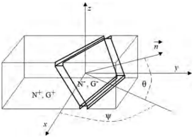
The Rice bifurcation theory[35]is used to predict the onset of plastic strain localization in the sheet metals studied. In this approach, bifurcation should be interpreted as the occurrence of a nonhomogeneous strain mode, in the form of an infi-nite localization band defined by its normal n!0, within a continuous medium that is subjected to a homogeneous strain state
(Fig. 17). Making use of the equilibrium and compatibility conditions, it is possible to derive the following localization criterion, namely the singularity of the acoustic tensor, which only involves the normal n!0 to the localization band and
the analytical tangent modulus L:
Fig. 17. Infinite localization band in the metal sheet at the moment of strain localization and the associated angles that defines the normal in the (X, Y) and (X, Z) plane.
detðn!0:L:n!0Þ ¼ 0: ð13Þ
The normal n!0can be defined geometrically in the (X, Y) and (X, Z) planes by the angles h and w (Fig. 17). In order to
com-pute the determinant of Eq.(13)for every time increment, the normal n!0is swept in the half range of the coordinates system
at intervals of 1#. This obviously implies that h
e
[0,p
) and we
[0,p
/2) due to the plane symmetry are considered for the sheet(finite element). As noted previously, the strain localization is reached when Eq.(13)reaches a global negative minimum which implies that the normal n!0takes a particular orientation defined by the two angles (h
min, wmin).
The analytical tangent modulus L is related to the elastic-plastic tangent modulus Cepby:
L ¼ Cepþ C1$ C2$ C3; ð14Þ
where C1, C2and C3are fourth-order tensors that can be expressed, after some mathematical derivations, as:
C1ijkl¼
R
ijdkl; C2ijkl¼1
2 ð
R
jldikþR
jkdilÞ; C3ijkl¼ 12 ð
R
ikdjl$R
ildjkÞ: ð15ÞNote that if the fourth order elasto-plastic tensor Cepis symmetric, the analytical tangent modulus L is not symmetric because of the contribution of the convective terms in Eq.(14). The elastic-plastic tangent modulus Cepis determined by
expressing the improved GTN yield function and the plastic multiplier in the Kuhn–Tucker form as follows:
U
GTN60;c
_ P0;U
GTNc
_¼ 0: ð16ÞThis form is convenient because it reveals that there is no plastic flow (i.e., _
c
¼ 0) whenUGTN< 0, while a strict plasticloading (i.e., _
c
> 0) necessarily implies that UGTN¼ 0 and _UGTN¼ 0. The latter represents the consistency condition, andcan be developed as follows:
_
U
GTN¼ VR: _Rþ Vr#r
_#þ Vf*_f*¼ 0: ð17ÞThe derivatives VR; Vr#and Vf* are obtained analytically in the following forms:
VR¼2 # r R#rþ q1q2f* 2 sinh 3 q2Rm 2 #r ' ( I ' ( ; Vr#¼ $2#r q # r % &2 þ 3q1q2f*Rm 2#r sinhð 3 q2Rm 2 #r Þ ' ( ; Vf*¼ 2 q1cosh 3 q2Rm 2 #r ' ( $ q3f* ' ( : 8 > > > > < > > > > : ð18Þ
The rate form of the hypo-elastic law allows us to express the stress rate in terms of the plastic multiplier _
c
:_
R¼ Ce:ðD $ _
c
VRÞ ¼ Cep:D: ð19ÞD is the macroscopic strain rate tensor. After some mathematical derivations involving the normality rule(10)and Eqs.(13) and (14), the elastic-plastic tangent modulus is obtained as follows:
Cep¼ Ce$ðC
e
:VRÞ # ðVR:CeÞ
Hc ; ð20Þ
where Hcis defined by the following relation: Hc¼ VR:C e :VR$ V#r @ #r @#ep ð1 $ f Þ R : VR #
r
$ Vf*dGTN An ð1 $ f Þ R : VR #r
þ ð1 $ f Þ VR:I * + : ð21Þ3.4.2. Numerical implementation of the model
The numerical algorithm for the integration of the GTN model is described in this section. The GTN model will be dis-cretized into incremental equations. We selected an implicit integration scheme for the GTN model since it is uncondition-ally stable, so convergence could be obtained for large time increments and therefore, a gain in the computation time could be achieved. The system of nonlinear equations is solved by the Newton-Raphson iterative method according to Ben Bettaieb et al.[36]at the Gauss point level. The procedure involves two steps: elastic predictor and plastic corrector. The total strain is decomposed into elastic and plastic parts:
e
¼e
eþ
e
pð22Þ
The total plastic strain increment is also separated into two parts:
D
e
p¼13
D
e
pI þD
e
qn ð23ÞD
e
p¼D
c
@U
GTN @R
m ð24ÞD
e
q¼D
c
@U
GTN @q ð25Þ n ¼3S2qis the flow direction for the isotropic material. Combining Eqs.(19) and (20)leads to the equality:
D
e
q@U
GTN @R
m þD
e
p@U
GTN @q ¼ 0 ð26ÞFrom the equivalence of the plastic work, one can deduce:
D
#e
p¼
R
mD
e
pþ qD
e
qð1 $ f Þ#
r
: ð27ÞFinally, from the expression of the rate of the void volume fraction, it can be written that
D
f ¼ fN sN ffiffiffiffiffiffiffi 2p
p exp $12 #e
p $e
N sN * +2 " #D
#e
p þ ð1 $ f ÞD
e
p ð28ÞIn the case of isotropic materials, the normal to the yield surface n is collinear to the direction of the deviatoric stress vector S. The system of Eqs.(6), (26)–(28)need to be solved numerically by using the Newton-Raphson iteration scheme. Accordingly, a trial elastic stress is first calculated by assuming that strain increment is purely elastic in the current time step. IfUGTN60,only the trail elastic stress is updated and one can proceed to the next time step. Otherwise, ifUGTN> 0,
the Newton–Raphson scheme is used to solve the set of equations described above. Four scalar variables (D
e
p;De
q;Df ;D#e
p) need to be determined at the end of each time step. Further details on the integration procedure andthe determination of the consistent tangent modulus can be found in[36], where representative benchmarks are fully patented. The relevant algorithm was implemented into the finite element code ABAQUS/Explicit as a user subroutine VUMAT. The state variable controlling the element deletion for the crack propagation is the cubic square of the localization criterion
ffiffiffiffiffiffiffiffiffiffiffiffiffiffiffiffiffiffiffiffiffiffiffiffiffi detðn!0:L:n!0Þ 3
q
. The element is deleted when this variable becomes less than or equal to zero.
3.4.3. Validation of the integration algorithm
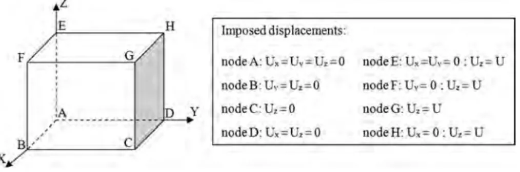
An essential step involves assessing the implemented integration algorithm of the GTN equations. Therefore, the GTN model is used to describe the deformation of one CPE4R finite element. The element is represented as a cube with an edge dimension of 1 mm and is subjected to uniaxial tension. The loading and boundary conditions imposed on the cube are pre-sented inFig. 18.
The material parameters for the Al5754 aluminum material identified in[33]are used in this simulation. In the latter framework, the Swift hardening law has been adopted for the matrix material[33]. The material parameters of the Swift model were fitted on the basis of the experimental stress–strain curve[37]. The material parameters of the GTN model are given inTable 2:
Fig. 19compares the numerical uniaxial response using the Abaqus GTN model and the response using the present GTN model integrated using the previously presented implicit algorithm (VUMAT). As shown in this figure, the responses obtained from implementation closely fit the Abaqus numerical curves. The onset of void coalescence is reached when the void volume fraction f becomes greater than the critical void volume fraction fc(fc= 0.00284) as indicated inFig. 19
(a) and (b). The material then softens and a stress drop is obtained as illustrated inFig. 19(a).
3.4.4. General procedure for parameters calibration
To evaluate the parameters of the CZM and GTN models, the nano-indentation and shear characterization tests of the assembly are related to their finite element models by using a parametric identification algorithm. The algorithm is based on the resolution of the inverse problem using a parametric calibration of the finite element model. First, the adopted method involves performing finite element simulations of the nano-indentation test in order to calibrate the parameters of the Swift law (n, K,
e
0). Then, the optimized values of (n, K,e
0) are fixed and used to simulate the shear tests in orderto calibrate the damage parameters of the GTN and CZM models. For each identification step, the unknown model param-eters vector x is determined in order to ensure good agreement between the numerical response of the model and the exper-imental data. Thus, an error function is defined which corresponds to the difference between the numerical and experimental responses that will be minimized using one or more optimization methods. This identification procedure is summarized inFig. 20. An initial model parameters set can be roughly determined provided that it gives the closest numer-ical response to the experimental data. The aim of this step is to minimize the computation time due to the numerous inverse problem iterations.
Table 2
Material parameters for the Al5754 aluminum material.
Junction E (GPa) m n K (MPa) e0 f0 fc q1 q2 q3 sN eN fN
Al5754 70 0.33 0.177 309.1 0.0017 10$3 0.00284 1.5 1 2.15 0.1 0.32 0.034
Fig. 19. Comparison of the numerical responses for the uniaxial tension issued from the predefined GTN model (Abaqus) and the implemented GTN model (VUMAT). (a) Stress strain curve and (b) evolution of the void volume fraction.
The resolution of the inverse parametric identification problem is performed by the Levenberg-Marquardt algorithm. The measurement of the error between the measured experimental response and the corresponding simulated value using the finite element model is taken through the calculation of the error function I given by Eq.(29).
I¼ ffiffiffiffiffiffiffiffiffiffiffiffiffiffiffiffiffiffiffiffiffiffiffiffiffiffiffiffiffiffiffiffiffiffiffiffiffiffiffiffiffiffiffiffiffiffiffi X Np i¼1 FNumi ðxÞ $ F Exp i FExp i !2 v u u t ð29Þ
FExprepresents the experimental measure of the reaction force and FNumrepresents the force obtained by the FE model. N p
is the number of points for the shear test and x is the vector of model parameters. After obtaining the best set of model parameters, a final verification procedure is performed to assess the accuracy of the parameters. Then, finite element sim-ulations of the shear test are conducted using a different geometry of the assembly. The dimension of the insert and the joint are increased from 3 mm ' 3 mm to 4.7 mm ' 4.7 mm in the case of the AuGe based assembly. Conversely, the metalliza-tions thickness is changed from 5 mm to 50 mm for the Ag nanoparticles assembly. The latter steps are essential as they enable validation of the accuracy of the selected parameters for simulations of assemblies under different geometries and loading conditions. Based on this method, the identified material parameters for the GTN damage model and for the hardening law providing a good fit to the experimental data for the different types of junction are summarized inTable 3.
4. Results and discussion
As abovementioned, the behavior of the system is quasi-static. A solver using an implicit numerical integration scheme is mainly used for the simulations. Nevertheless, the main limits could be the difficulty in converging this solver up to the total rupture of the rupture zone, especially when the fracture energy is small; in other words, brittle damage occurs in the inter-faces. This results in a major disadvantage in the identification procedure since it is not possible to fully construct the force-displacement curve used to form the residual vector. In addition, element deletion cannot be recovered for the solid joint with the implicit solver, and crack propagation therefore cannot be observed. To solve this problem, we used a solver with an explicit numerical integration scheme (Abaqus/Explicit); these solvers have a considerable robustness within strong non-linearities. The explicit solver permits the use of the element deletion technique, which enables the representation of the discontinuity by gradual element deletion from the mesh. The element status is linked to a state variable, of which the default value is 1. When the state variable was equal to 0, the associated element is deleted by prescribing a zero stress state within the element. However, using an explicit solver, excessive computational times and oscillating force due to stress wave propagation in the element may be exhibited. To overcome this obstacles, a time scaling factor of 10$6is adopted.
Fig. 21shows the nano-indentation and shear force-displacement curves obtained for the two types of assemblies. Good agreement between the experimental data and numerical results are recorded. With the set of parameters presented, the explicit solver allow the complete construction of the curve. For the Cu/Cu assembly with the AuGe alloy, the experimental and numerical shear responses are close, provided that the crack is not initiated. Beyond an overall displacement of the order of 0.13 mm and a force of 770 N, the numerical curve drops with a combined interface/solder cracking. The rupture failure with the numerical model is slightly faster than that of the experimental system as the acceleration factor deduced from the critical void volume fraction is slightly overestimated.
For sintered silver nanoparticle joints, the numerical force displacement response closely matches the experiment result since the crack propagates rapidly in the brittle Ag metallization. Therefore, small plasticity is recorded for the silver nanoparticles joint that is concentrated in the nanoparticles layer borders. In this case, the straightforward rupture on the test is fairly well represented by the numerical model.
Fig. 22illustrates the results of the Von Mises equivalent stress distributions at the final state (total failure) in the differ-ent layers of the assemblies studied. Naturally, interest is only focused on layers where damage is observed and/or crack have occurred. This means that only the cohesive elements layers and the joint are represented.Fig. 22(a) illustrates the final crack appearing in the Cu/Cu assembly performed with the AuGe solder. A very short time is recorded between the initiation and total failure of the junction. The crack initiation is produced at the left side of the junction in a small portion of the cohe-sive layer. It then propagates in the middle of the junction inside the solder layer until total failure. Other very small cohecohe-sive delaminations are dispersed along the junction width. This numerical result is in agreement with the experimental observations shown inFig. 7where traces of Au and solder are detected on the insert surface using EDX spectroscopy.
Table 3
Material parameters of GTN model and the cohesive zone model for the studied junctions.
Junction E (GPa) m n K (MPa) e0 f0 fc q1 q2 q3 sN eN fN Ec (GPa) Gc t0 AuGe/Au finish 80 0.32 0.3 960 2.'10$3 10$3 1.147 ' 10$3 1.5 1 2.25 0.1 0.27 0.11 20 0.01 230 Ag nano/Ag finish 70 0.3 0.17 200 2.'10$3 10$1 0.101 1.5 1 2.25 0.1 0.27 0.35 1 0.01 30 Cu 115 0.36 0.19 297 3.7 ' 10$3 –
The experimental result showed a mixed fracture of the solder layer and Au metallization. As shown inFig. 22(b), a crack initiates first at the Ag nanoparticles layer in both the right and left sides of the joint and across the entire thickness. The crack then propagates rapidly in the bottom Ag interface until total failure of the assembly. Therefore, the major part of the crack is located on the Ag interface leaving a small amount of Ag nanoparticles on the top of the substrate. This observed phenomenon corroborates the obtained fracture faces of the Ag nanoparticles/Ag assemblies where the Ag nanoparticles are detected over almost the entire surface of the insert, while only leaving two small Ag areas near the insert borders.
Fig. 23shows the distribution of the volume fraction of voids f in the AuGe and Ag nanoparticles joints. For the AuGe joint, a crack propagates from the left side to the right side of the junction. Elements deletion first acts in the left side of the solder joint along the interface neighbor. Then, the cracking path changes the direction to a privileged orientation (i.e. the middle of the junction), and finally deviates again towards the cohesive layer at the right side of the junction until total failure. For the Ag nanoparticles joint, a small crack occurs at the borders of the layer and evolves towards the bottom interface of the junc-tion (Fig. 23(b)). The Ag nanoparticles layer has a high initial void volume fraction f0(0.1) which is very close to the critical
void volume fraction fc(0.101). Therefore, the early cracking of the joint is due to the rapid increase of the void volume
frac-tion from f0to fc. The volume fraction of voids is high at the borders and at the middle of the joint since a significant amount
of plastic deformation is recorded early at these regions.
Fig. 24corroborates the previously exposed comments and illustrates the evolution of damage or the void volume frac-tion f obtained by finite element simulafrac-tions against the undeformed juncfrac-tion width. The figure shows that most of the dam-age occurs at the left side of the AuGe joint (Fig. 24(a)). The void volume fraction takes a value of 9.5 ' 10$4smaller than f
0
(f0= 10$3) in the right side corner of the solder layer (distance of 3 mm along path). This is due to the compressive stress
generated in this junction area. For the Ag nanoparticles layer, the fracture occurs on the borders of the junction.Fig. 24
(b) also shows that the highest void volume fractions are recorded in these areas. Since the initial void volume fraction is
Fig. 21. Comparison between experimental data and calibrated force displacement responses. (a) Nano-indentation tests and (b) shear tests.
Fig. 22. Final crack configurations of the Cu/Cu assemblies and Von Mises stress distribution in the different junction layers. (a) AuGe/Au finish assembly and (b) Ag nanoparticles/Ag finish assembly.
close to the critical void volume fraction for both the AuGe and Ag nanoparticles junctions, the crack initiates and propagates rapidly, since the coalescence stage appears early.
Fig. 25shows the evolution of the cubic square of the localization criterion against strain for the first failed element of the AuGe and Ag nanoparticles joints. The bifurcation theory needs to be used with a damage model (GTN in this case) in order to obtain softening (stress drop). The localization criterion is the principal indicator of the failure in the material. Indeed, this condition depends on the stress state which, in turn depends of the void volume fraction. In the first stage of loading, the criterion considerably decreases as the stress increases due to the elastic and plastic deformation. Subsequently, the criterion stabilizes rapidly when the stress reaches a steady state, indicating the approach of coalescence. At the moment of the strain localization (onset of coalescence), the material begins to soften, a drop of stress is generated and the localization criterion decreases again until zero value at total failure. At this time, the element is deactivated (fail). Therefore, the localization cri-terion detðn!0:L:n!0Þ is considered as the state variables controlling the element deletion.
Fig. 23. Distribution of void volume fraction in the joint layer during initiation and propagation as well as at the total failure of the joint. (a) AuGe/Au based assembly. (b) Silver nanoparticles based assembly.
Fig. 24. Evolution of the void volume fraction f along a path crossing the joint layer during initiation and propagation as well as at the total failure of the joint. (a) AuGe/Au based assembly. (b) Ag nanoparticles based assembly.
Fig. 26shows the evolution of stress in the first cohesive element undergoing failure. Debonding begins when the stress reaches its maximum value and is completed when the stress reaches a zero value. The evolution of debonding from the ini-tiation to the complete failure is very rapid as demonstrated by the vertical drop of the stress. The Au interfaces response (AuGe solder based assembly) is nonlinear as the fracture energy and the magnitude of the stress vector of the interface ele-ment are high. Subsequently, the Ag interface (Ag nanoparticles based assembly) is very brittle. It undergoes just a small straining before element failure since the magnitude of the stress vector in this case is considerably small.
Some concerns could arise about the accuracy of the identified model parameters and their ability to represent material behavior in a different geometry or configuration of the shear assembly. Therefore, additional shear tests are performed using the two types of junctions previously modeled using finite element simulations. In the present simulations, the same loading and boundary conditions are adopted. Nevertheless, for the AuGe based assembly, the dimension of the insert is
Fig. 25. Strain localization condition until total failure of the material, extracted in the first failed element in the joints.
Fig. 26. Von Mises stress in the first element of the cohesive layer undergoing deletion. The figure shows both cases of AuGe/Au and Ag nanoparticles/Ag assemblies.
increased from 3 mm ' 3 mm to 4.7 mm ' 4.7 mm. Consequently, the associated cohesive layers and joint follow the same change in dimensions. For the Ag nanoparticles based assembly, the thickness of the metallizations is modified. Henceforth, it takes the value of 50 mm instead of 5 mm. Moreover, copper is replaced by a purely elastic diamond as the insert material. This enables the present configuration to be closer to the real configuration. The numerical results and the experimental data are compared in terms of force displacement curves.Fig. 27shows the force displacement curves of the relevant shear tests. The finite element modeling gives correct general trends but slightly underestimates the force level for the two types of assemblies. Higher forces are recorded for these assemblies as the geometric and material configuration changed. For the AuGe based assembly, the surface of contact between the different layers increased considerably leading to an increase of the reaction force. In the Ag nanoparticles assembly, replacing copper with diamond leads to a small increase of the exper-imental shear force from 230 N to 280 N. A small variation of the numerical force is observed which is due to a change in the crack direction. Progressive softening then occurs until total failure of the assembly.
5. Conclusion
To study the crack initiation and propagation in power electronic assemblies, shear lap specimens are manufactured and subjected to micro-shear tests. The specimen consists of an Ni/Au or Ag metallized copper stud which is assembled into an Ni/Au or Ag metallized copper substrate using two types of joints: AuGe alloy joint and Ag nanoparticles joint. The experimen-tal data obtained at room temperature showed that, for the AuGe based junction, the cracks propagate evenly along the sur-face of the joint and the intersur-face, leading to a total break in the middle of the junction. The SEM and EDX fractography analyses show almost a mixed fracture: adhesive in the two Cu/solder interfaces and cohesive in the joint. However, the Ag nanoparticles based junction shows a failure mainly produced at the bottom Ag interface after a small initiation in the Ag nanoparticles joint. The SEM and EDX fractography analyses show a failure face advancing almost along the entire surface of the interface. For the two types of junction, the crack propagation is rapid either in the solder layer or in the Ag interface, as the latter is very brittle. Finally, regarding the obtained results from experiments, it seems that the soldering technique using AuGe alloy is the most convenient solution for power electronic components undergoing temperatures up to 125 #C. Moreover, the deposited Ag metallization performed on the copper stud and substrate is compatible with the solder compo-nents. Therefore, the junction formed with the AuGe solder layer and Ag metallization presents better mechanical behavior compared to the brittle junction formed with Ag nanoparticles and Ag metallization. The fragile aspect of the Ag nanoparti-cles junction is due to the poor quality of the interface between the Ag metallization and the Ag nanopartinanoparti-cles layer, even though the Ag nanoparticles layer presents good mechanical and thermal properties. To take further advantages of this Ag junction, the parameters of the sintering process may need to be better controlled in order to improve the solid diffusion of the Ag present in the substrates and the nanoparticles layer. Finite element modeling of the micro-shear tests is performed by using a bilinear CZM parameters for the Cu/AuGe and the Cu/Ag nanoparticles interfaces. A GTN damage model is coupled to the Rice bifurcation theory to describe damage initiation and propagation in the joints. The interfacial fracture of these assemblies was then simulated using 2D finite element modeling. The models parameters were identified using the inverse method involving the additional nano-indentation data, shear data and iterative finite element simulations. The obtained results show good agreement between the experimental data and the numerical responses. The coupled model demon-strated its ability to describe the mechanical behavior of the junctions until the strain localization. Finally, finite element simulations are needed to assess the behavior of the AuGe and Ag junctions during thermal cycling and to predict the lifetime of the obtained power electronics assemblies. Microstructural changes must be thoroughly studied in order to determine rupture mechanisms under cyclic thermal conditions. The parameters for the elaboration process have a direct influence on the thermomechanical behavior of the packaging. Therefore, an investigation of the effect of these control parameters is required mainly to overcome the causes of cracking in the elaborated electronic devices.
References
[1] Adams P. Thermal fatigue of solder joints in micro-electronic devices [Ph.D. Thesis]. Massachusetts Institute of Technology; 1986. [2]Chelnokov V, Syrkin A. High temperature electronics using SiC: actual situation and unsolved problems. Mat Sci Eng B 1997;46:248–53. [3]Ciappa M. Selected failure mechanisms of modern power modules. Microelectron Reliab 2002;42:653–67.
[4]Yao Y, Vaynman S, Keer LM, Fine ME. Energy-based micromechanics analysis on fatigue crack propagation behavior in Sn-Ag eutectic solder. J Electron Mater 2008;37:339–46.
[5] Müge E. Thermomechanical fatigue failure of interfaces in lead-free solders [Ph.D. Thesis]. Eindhoven University of Technology; 2007. [6]Needleman A. A continuum model for void nucleation by inclusion debonding. J Appl Mech 1987.
[7]Tvergaard V, Hutchinson JW. The relation between crack growth resistance and fracture process parameters in elastic-plastic solids. J Mech Phys Solids 1992;40:1377–97.
[8]Xu XP, Needleman A. Numerical simulations of fast crack growth in brittle solids. J Mech Phys Solids 1994;42:1397–434. [9]Camacho G, Ortiz M. Computational modelling of impact damage in brittle materials. Int J Solids Struct 1996;33:2899–938. [10]Zavattieri P, Espinosa H. Grain level analysis of crack initiation and propagation in brittle materials. Acta Mater 2001;49:4291–311.
[11]Tvergaard V, Hutchinson JW. Two mechanisms of ductile fracture: void by void growth versus multiple void interaction. Int J Solids Struct 2002;39:3581–97.
[12]Alfano G. On the influence of the shape of the interface law on the application of cohesive-zone models. Compos Sci Technol 2006;66:723–30 [Advances in statics and dynamics of delamination. Workshop on Advances in Modeling Delamination in Composite Materials and Structures]. [13]Scheider I. Micromechanical based derivation of traction-separation laws for cohesive model simulations. Procedia Engineer 2009;1:17–21
[14]Ren HH, Wang XS, Jia S. Fracture analysis on die attach adhesives for stacked packages based on in-situ testing and cohesive zone model. Microelectron Reliab 2013;53:1021–8.
[15]Yao Y, Keer LM. Cohesive fracture mechanics based numerical analysis to BGA packaging and lead free solders under drop impact. Microelectron Reliab 2013;53:629–37.
[16]Wippler S, Kuna M. Experimental and numerical investigation on the reliability of leadfree solders. Eng Fract Mech 2008;75:3534–44 [Local Approach to Fracture (1986–2006): Selected papers from the 9th European Mechanics of Materials Conference].
[17]Kuna M, Wippler S. A cyclic viscoplastic and creep damage model for lead free solder alloys. Eng Fract Mech 2010;77:3635–47 [Computational Mechanics in Fracture and Damage: A Special Issue in Honor of Prof. Gross].
[18] Zhang L, Sitaraman R, Patwardhan V, Nguyen L, Kelkar N. Solder joint reliability model vath modified Darveaux’s equations for the micro SMD wafer level-chip scale package family. In: 53rd Electronic components and technology conference, 2003. Proceedings; May 2003. p. 572–7.
[19]Chen S, Sun P, Wei X, Cheng Z, Liu J. Coffin-Manson equation of Sn-4.0Ag-0.5Cu solder joint. Solder Surf Mt Tech 2009;21:48–54. [20] Stolkarts V, Keer LM, Fine ME. Constitutive and cyclic damage model of 63Sn-37Pb solder. J Electron Packag 2000;123:351–5. [21]Ye H, Lin M, Basaran C. Failure modes and FEM analysis of power electronic packaging. Fin Elem Anal Des 2002;38:601–12.
[22]Chan D, Subbarayan G, Nguyen L. Maximum-entropy principle for modeling damage and fracture in solder joints. J Electron Mater 2012;41:398–411. [23]Towashiraporn P, Subbarayan G, Desai C. A hybrid model for computationally efficient fatigue fracture simulations at microelectronic assembly
interfaces. Int J Solids Struct 2005;42:4468–83.
[24]Cocks ACF, Ashby MF. Intergranular fracture during power-law creep under multiaxial stresses. Metal Sci 1980;14:395–402.
[25]Eftis J, Nemes J. Evolution equation for the void volume growth rate in a viscoplastic-damage constitutive model. Int J Plast 1991;7:275–93. [26]Lee Y. Modeling ductile damage evolution in metal forming processes. Cornell University; 1991.
[27]Gurson AL. Continuum theory of ductile rupture by void nucleation and growth: Part I-yield criteria and flow rules for porous ductile media. J Eng Mater Technol 1977;99:2–15.
[28]Tvergaard V, Needleman A. Analysis of the cup-cone fracture in a round tensile bar. Acta Metall Mater 1984;32:157–69.
[29]Hao S, Brocks W. The Gurson-Tvergaard-Needleman-model for rate and temperature-dependent materials with isotropic and kinematic hardening. Comput Mech 1997;20:34–40.
[30] Hornberger J, Mounce S, Schupbach R, McPherson B, Mustain H, Mantooth A, et al. High-temperature integration of silicon carbide (SiC) and silicon-on-insulator (SOI) electronics in multichip power modules (MCPMs). In: 2005 European conference on power electronics and applications; Sept 2005. p. 10 pp–P. 10.
[31] Nagatomo Y, Nagase T. The study of the power modules with high reliability for EV use. In: Conference 17th EVS; 2000.
[32]Camanho PP, Davila CG, De Moura MF. Numerical simulation of mixed-mode progressive delamination in composite materials. J Compos Mater 2003;37:1415–38.
[33]Mansouri LZ, Chalal H, Abed-Meraim F. Ductility limit prediction using a GTN damage model coupled with localization bifurcation analysis. Mech Mater 2014;76:64–92.
[34]Chu CC, Needleman A. Void nucleation effects in biaxially stretched sheets. J Eng Mater Technol 1980;102:249–56. [35] Rice J. Theoretical and applied mechanics; 1976. p. 207–27 [chap. The localization of plastic deformation].
[36]Bettaieb M Ben, Lemoine X, Duchêne L, Habraken AM. On the numerical integration of an advanced Gurson model. Int J Numer Meth Eng 2011;85:1049–72.
[37]Brunet M, Mguil S, Morestin F. Analytical and experimental studies of necking in sheet metal forming processes. J Mater Process Tech 1998;80– 81:40–6.