HAL Id: hal-03200777
https://hal.archives-ouvertes.fr/hal-03200777
Submitted on 16 Apr 2021
HAL is a multi-disciplinary open access
archive for the deposit and dissemination of
sci-entific research documents, whether they are
pub-lished or not. The documents may come from
teaching and research institutions in France or
abroad, or from public or private research centers.
L’archive ouverte pluridisciplinaire HAL, est
destinée au dépôt et à la diffusion de documents
scientifiques de niveau recherche, publiés ou non,
émanant des établissements d’enseignement et de
recherche français ou étrangers, des laboratoires
publics ou privés.
coupler based on Focused Ion Beam Milled Bragg
reflectors
Kamal Ghoumid, Badr-Eddine Benkelfat, Richard Ferriere, Gwenn Ulliac,
Tijani Gharbi
To cite this version:
Kamal Ghoumid, Badr-Eddine Benkelfat, Richard Ferriere, Gwenn Ulliac, Tijani Gharbi.
Wavelength-selective Ti:LiNbO3 multiple Y-Branch coupler based on Focused Ion Beam Milled Bragg reflectors.
Journal of Lightwave Technology, Institute of Electrical and Electronics Engineers (IEEE)/Optical
Society of America(OSA), 2011, 29 (23), pp.3536 - 3541. �10.1109/jlt.2011.2170056�. �hal-03200777�
Wavelength-Selective Ti:LiNbO Multiple
Y-Branch Coupler Based on Focused Ion
Beam Milled Bragg Reflectors
Kamal Ghoumid, Badr-Eddine Benkelfat, Senior Member, IEEE, Richard Ferriere, Gwenn Ulliac, and Tijani Gharbi
Abstract—This paper described a wavelength-selective couplers
dedicated to drop functionality (spectral-selective couplers dedi-cated to wavelength demultiplexing). It is consist of two Y junc-tions: an input two drop channels and an output. The Y-branches distributors of optical power were carried out by a specific geom-etry of Ti:LiNbO waveguides. Each Y junction is composed by two identical bends jointed at one with a weak inclination angle to decrease losses. On each arm of the Y-branches, a Bragg grating (BG) is etched by Focused Ion Beam (FIB) in order to extract a specific wavelength band. A two-channel configuration is adopted which demonstrate a drop functionality of two spectral bands cen-tered at 1123 nm and 1527 nm. The complementary spectrum is avalaible at the coupler output.
Index Terms—Bragg reflectors, drop channels, wavelength
fil-tering devices, Y-branch coupler.
I. INTRODUCTION
D
ENSE and Coarse Wavelength Division Multiplexing (WDM) technologies, for metro and access networks, are some applications based on the use of specific optical devices. In the last decade, these optical networks are rapidly evolved from static to dynamic architectures. The critical component in a reconfigurable network is the Reconfigurable Optical Add/Drop (ROADM) which require flexibility in the optical wavelength domain, based on Wavelength Selective Switching (WSS).A wavelength selective switch is an optical device that routes different spectral components from an input port to the desired output ports without optical-to-electrical-to-optical conversion. In this context, several approaches have been proposed for implementation of the WSS subsystem. Most of them have
Manuscript received February 03, 2011; revised June 21, 2011; accepted September 21, 2011. Date of publication September 29, 2011; date of current version November 25, 2011.
K. Ghoumid is with École Nationale des Sciences Appliquées d’Oujda, ENSAO, 60000 Oujda, Morocco, and also with Institut Femto-ST Dé-partement (LOPMD) UMR CNRS 6174, Université de Franche-Comté, 25030 Besançon Cedex, France (e-mail: kghoumid@ensa.univ-oujda.ac.ma; kamal.ghoumid@univ-fcomte.fr).
B.-E. Benkelfat is with Institut TELECOM, TELECOM Sud-Paris, Samovar UMR, INT-CNRS 5157, 91011 Evry Cedex, France (e-mail: Badr-Eddine.Benkelfat@int-edu.eu).
R. Ferriére, G. Ulliac, and T. Gharbi are with Institut Femto-ST Dé-partement d’Optique P.M. Duffieux (LOPMD) UMR CNRS 6174, Univer-sité de Franche-Comté, 25030 Besançon Cedex, France (e-mail: richard. ferriere@univ-fcomte.fr; gwenn.ulliac@univ-fcomte.fr; tijani.gharbi@univ-fcomte.fr).
Digital Object Identifier 10.1109/JLT.2011.2170056
mainly focused on Liquid Crystal on Silicon (LCoS) and Micro-Electro-Mechanical-System (MEMS) technologies [1], [2].
In a conventional WSS, the optical performance (e.g., channel spacing, filter shape, etc.) is determined by the physical design of the optical structure through which the light passes. More recently, an add/drop filter based on coupled vertical gratings on silicon has been proposed to implement 1 by 4 WDM functionality [3]. The realization of such applications in integrated optics opens several applications.
Integrated optical components using Y-branch structures are used in such applications, are commonly employed in recent years like, for example, to realized Mach–Zehnder modulators [4], [5], or 1 2 digital optical switch known as “Y-branch dig-ital optical switch” (DOS) [6]–[8]. Specific function, like vari-able power ratio division or TE/TM mode conversion, can be realized by using the electro-optic properties of lithium niobate (LN, LiNbO ) [9]. Wavelength filtering can also be obtained by surface acoustic wave (SAW) on LN. Furthermore, with an asymmetrical Y-junction structure fabricated by diffusing dif-ferent materials into Y-cut LN, the incident TE and TM modes can be split by two output arms due to their different preferences of polarizations [10]. More recently the propagation in two-di-mensional photonic crystal slabs allows an amplitude division of a guided beam [11].
The lithium niobate crystal stays a popular material for inte-grated optics, mainly due to its electro-optical, acousto-optical and non-linear properties that are exploited on various com-mercial devices [12]–[15]. It needs relatively simple techniques to obtain good performances compared with the sophisticated technologies used for semiconductor materials. The use of such a material is recommended in several integrated components.
The micro/nano-structuring of LiNbO for the manufacture of BGs represents however a challenging task, due to the well known resistance of the material to standard machining methods [16]–[20]. Different approaches have been conducted for achieving nanostructures are employed [21]–[23]. The possibility of realizing miniature LiNbO components arises with these fabrication methods.
In this article, FIB method is implemented to etch BGs on Ti:LiNbO waveguides [24], [25] whose geometrical structure is composed by Y-branch junctions, in order to extract spectrum bands in awideband optical source. We chose this technique be-cause we have already shown its effectiveness in achieving the proper Bragg reflectors with reflection coefficients that reach 97%, associated with bandwidth midheight width of about 0733-8724/$26.00 © 2011 IEEE
Fig. 1. Wavelength selectif coupler composed by two Y junctions cascading: an input , two drop channels , and output , including two Bragg gratings and on each arm.
100 nm [21], [22]. This method has already been employed to etch sub-micrometric one-dimensional structures in LiNbO or 2D-photonic crystals. In comparison with more standard methods, FIB milling the advantage concerne the direct etching without any additional technological steps. Indeed FIB is a high capacity tool providing direct, local and controlled waveguide property modifications [24], [25].
Here we show the feasibility and the realization of a spe-cific coupler using as a wavelength filter which consist of two Y-branches and two BGs in order to extract spectrum bands in a wideband optical source. Our idea was based on the properties of BGs that are used generally to achieve very high reflection around a given central wavelength. Thus, at the first two out-puts, two spectral bands around 1123 nm and 1527 nm are ex-tracted by the mean of BGs. At the output, the complementary spectrum of the input source is available. This component could have a significant interest in convenient and reproducible fab-rication technologies, ‘The benefit of the proposed structure is that can be used as the switching element for wavelength routing in a wavelength selective switch.
We will consider as the future prospects will be to benefit from eletro-optical properties of LN for realizing tunable devices, that would be very useful and convenient for the switching element for wavelength routing in a Wavelength Selective Switch.
II. PRINCIPLE OFWAVELENGTHDEMULTIPLEXING BY MULTIPLEY-BRANCHCOUPLER
We present a wavelength-selective coupler; the common property desired in this type of device is the extraction of pecu-liar wavelengths from a continuum. Its basic scheme is given in Fig. 1; it consists in an input E and three outputs and . Two Bragg gratings noted and were etched in each arm of the Y junctions, they reflect the wavelengths around and respectively. The other wavelengths are transmitted and not affected by the BG.
If a continuous spectrum is injected at E, a wavelength bands reflected around and are recovered at and due to and respectively. It is obtained by the mean of a “white” fiber laser. At output, the entire spectrum is transmitted, except for the reflected bands. It should be noted
that the wavelengths reflected around and recovered at have a power less than those recovered at , this is due to the alignment losses. We also note that the output , the presence a small portion of the spectrum reflected wavelengths around due to .
We recall that the wavelengths reflected obey the Bragg con-dition given by following equation [26]–[28]:
(1) where is the effective index of the propagating mode in the waveguide, and are respectively the Bragg order and period. is the Bragg wavelength.
III. FABRICATIONPROCESS
The preliminary experiments were carried out on a LiNbO chip with a thickness of 0.5 mm and X-cut Z-propagation is used as substrate. In this configuration the two polarizations TE/TM of incident wave are affected by the same index
nm during its propagation. A Titanium layer (90 nm thickness) is deposited on the crystal surface by means of an Alliance Concept Eva 450 sputtering. The evaporation speed in the chamber is controlled by an Inficon quartz oscillator which assures a homogenous deposition of the metal. The geo-metric pattern of waveguides is realized by classical photolitho-graphic techniques and chemical etching of the titanium layer. The optical waveguides are obtained by standard thermal indif-fusion (1020 C during 8 h) of titanium ribbons (90 nm-thick and 7 m wide). The thermal diffusion of the titanium layer causes a variation of the refractive index of LN proportional to the con-centration of Ti. Therefore, we obtain an increase in ordinary and extraordinary indexes of LiNbO . Thus, the resulting layer is described as an index which is greater relatively to those of adjacent layers. It allows the confinement of light, and hence the realization of the waveguide Ti:LiNbO . The guiding layer is of an index gradient, it is designed to reduce scattering losses due to interface roughness, and also to minimized the modal and polarization dispersion of the optical mode traveling in the waveguide.
With these experimental parameters the refractive in-dexes of the waveguide and the adjacent layers are:
nm
nm nm
nm . In addition, it is worth noting that the waveguide is single mode obtained in the range of wavelengths [1050–1600] nm (with cutoff wave-length nm). The profile observed on a monitor via an infrared camera is shown in Fig. 2. These dimensions measured at relatively to its maximum are m and
m, and its maximum is measured at m.
A top views of Ti:LiNbO waveguide and the two Y-branches are represented on the Fig. 3. It is noted that the two Y junc-tions are designed with an inclination angle in order to avoid significant propagation losses in the waveguide splitter [29]–[31]. In our conception, the angle of inclination of the arms is even lower than this value, it is 0.6 .
Once the waveguides were manufactured, the following step deals with the etching of and . The FIB method was
Fig. 2. The profile of the mode propagated in the plan of Ti:LiNbO waveguide observed on a monitor TV via an infrared camera. It is single-mode at the wavelength 1550 nm.
Fig. 3. (a) First junction Y, (b) second junction Y, (c) Ti:LiNbO waveguide obtained by standard diffusion (90 nm thick and 7 m wide titanium layers at 1020 C during 8 h).
adopted to realize a micro-structuration of the waveguides. FIB technique produces a localized sputtering of the material. Consequently it induces significant transformations of the guide structure and a strong modification of the propagation prop-erties. In these experimentations a dual beam Orsay Physics
Canion 31 LEO 4400 FIB was used, the command of the beam deflection was realized by a Raith Elphy Quantum 4.0 driver. Starting with the sputtering of a Chromium Cr layer whose main role is to prevent the accumulation of Ga ions, with a thickness of 12 nm on the substrate, which was then inserted into the FIB chamber and exposed to a Ga liquid metal ion source (LMIS) with ion acceleration energy of 30 keV.
For the design of both BGs, we used (1), with the Bragg order and nm. As a result, we obtain the following parameters: the first has a period m, a period number and an etching depth m, whereas the second (with
and nm) has a period m, a period number and an etching depth m. The BG obtained by FIB etching is illustrated in Fig. 4.
It should be noted the etching depth of the FIB process ( m) doesn’t match the modal depth of the Ti diffused waveguides (about 2.2 m evaluated at of maximum mode intensities [21]). This means for sure reduced grating effective-ness and additional out of plane losses. At this etching depth m, we expect an improvement of losses of in order of about 2.2 dB compared to the same BG the same quality but etched up to a depth of m.
IV. RESULTS ANDDISCUSSIONS
To assess the spectral responses in each output, a continuous spectrum source with a wavelength range of nm is launched at the coupler input. This continuum laser uses a strong nonlinear effect induced by a picosecond pulse (1064 nm) in-jected in a photonic crystal fiber specially designed [32]. It al-lows to obtain radiation with a flat broadband spectrum from nm. The measurement setup included: The mea-surement setup included: elements (V-grooves : ) for the injection and recovery of transmitted and reflected tical signals, waveguide + selectif coupler, as well as three op-tical spectrum analysers and to measure reflectivities and the transmittances respectively (Fig. 5).
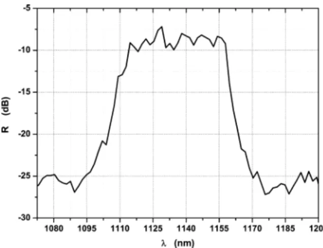
Figs. 6 and 7, illustrate the reflectivities curves versus wave-lengths measured at the outputs and respectively, they were centered around nm and nm. The coefficients of reflection of each curve were measured and found about 95%. The bandwidth at half maximum are respectively
nm and nm.
Fig. 8 shows the measured transmission spectrum at the output versus wavelengths of the signal of our device, and the whole transmitted spectrum was obtained except for the reflected wavelengths. It should be noted that the reflectance PSD and transmittance PSD are not the exact reciprocal of each other (because of the loss, absorption ).
This study of experimental measurements implies the an-nouncement of the existence of various types of losses which is related to: the injection and alignment process, material absorp-tion, Y-junctions (inclination) and Bragg gratings corrugations. In the absence of corrugations, the three first types of front losses mentioned, can be estimated from Fig. 8 to be around 6 dB (this value is found to be the mean difference between curves (a) and (b)). The losses due to etching can be estimated
Fig. 4. (a) m, m) etched in a Ti:LiNbO waveguide by FIB, (b) zoom of and Ti:LiNbO waveguide.
between 2 and 2.5 dB (the mean difference between curves (b) and (c)) [21].
A good results should be pointed out, a nice and non trivial feature of the presented experimental results is the absence of parasitic coupling to cladding modes, that usually induce un-wanted losses at wavelengths shorter than the nominal one.
A significant remark concerning the existence of the parasitic peaks in the spectra of the reflectivities or of the transmittance measured at the exits and , which are due to the rough-ness of the holes obtained after etching by FIB [21]. Indeed, by the engraving of a material by the mean of the FIB, the later is
Fig. 5. Experimental setup : continuous spectrum [850–1750] nm, V-grooves , optical fibers (O.F.), waveguide + selectif coupler and
and .
Fig. 6. Reflectivity versus wavelengths measured at the output : peak cen-tered around nm with nm.
Fig. 7. Reflectivity versus wavelengths measured at the output : peak cen-tered around nm with nm.
insulated by Ga ions, these induced modifications by the ionic insulation seems to be insignificant and the reason of the imper-fections in the transmitted spectra and the Optical propagations is certainly due to the conical shape of the engraved BGs [33] and does not seem to be a modification of the substrate from the insulation.
Fig. 8. Transmission versus wavelengths measured at the output . The peak at 1064 nm corresponds to the pump of the ‘white’ laser employed to provide the wide spectrum at E input. (a) Source ‘white’ laser, (b) Ti:LiNbO waveguide, (c) measured spectrum at the output .
V. CONCLUSION
A concrete application for extraction of wavelength bands by using Ti:LiNbO waveguides with two Y junctions, com-prising an input and a several outputs had been clearly demon-strated. The waveguides were manufactured by thermal diffu-sion process, and the Bragg gratings were etched by FIB in each Y-branch. Thus, a successful extraction from the bands around 1123 nm and 1527 nm was achieved. The principal advantages of this directional coupler, is that it can be used in both direc-tions. Moreover, it can contain several Y junctions and sev-eral BGs, in order to extract other wavelengths. Nevertheless, we noted that the milling process of BGs was very long (eight hours).
Our perspective is to design, manufacture and characterize this kind of components suited for applications like DWDM. We will seek to remove wavelengths below 1 nm by changing the BGs parameters used for obtaining highly selective filters. Another objective will be to benefit from eletro-optical prop-erties of LN for realizing tunable devices that would be very useful and convenient in practical applications. Also, we note that this structure can be used in an application in the field of optical networks.
ACKNOWLEDGMENT
The authors wish to acknowledge R. Salut, B. Guichardaz, D. Bitschene, J.-Y. Rauch, V. Petrini for technical assistance, and all personnel of the MIMENTO technology centre of the Institut FEMTO-ST, Besançon, France.
REFERENCES
[1] Y. Sakurai, M. Kawasugi, Y. Hotta, S. Khan, H. Oguri, K. Takeuchi, S. Michihata, and N. Uehara, “LCOS-based 4 4 wavelength cross-con-nect switch for flexible channel management in ROADMs,” in Proc.
Opt. Fiber Commun. Conf., Los Angeles, CA, Mar. 6, 2011, pp. 1–3.
[2] T. A. Strasser and J. L. Wagener, “Wavelength-selective switches for ROADM applications,” IEEE J. Sel. Topics Quantum Electron., vol. 6, no. 5, pp. 1150–1157, 2010.
[3] D. T. H. Tan, K. Ikeda, S. Zamek, A. Mizrahi, M. P. Nezhad, A. V. Krishnamoorthy, K. Raj, J. E. Cunningham, X. Zheng, I. Shubin, Y. Luo, and Y. Fainman, “Wide bandwidth, low loss 1 by 4 wavelength division multiplexer on silicon for optical interconnects,” Opt. Exp., vol. 19, no. 3, pp. 2401–2409, 2011.
[4] Q. Zhou, J. Yang, Z. Shi, Y. Jiang, B. Howley, and R. T. Chen, “Perfor-mance limitations of a Y-branch directional coupler-based polymeric high-speed electro-optical modulator,” Opt. Eng., vol. 43, no. 4, pp. 806–811, 2004.
[5] D. An, Z. Shi, L. Sun, J. M. Taboada, Q. Zhou, X. Lu, R. T. Chen, S. Tabg, H. Zhang, W. H. Steier, A. Ren, and L. R. Dalton, “Polymeric electro-optic modulator based on 1A2 Y-fed directional coupler,” Appl.
Phys. Lett., vol. 76, no. 15, pp. 1972–1974, 2000.
[6] W.-C. Chang and H.-C. Hou, “Switching characteristics of Ni:LiNbO directional couplers with two types of waveguide structures,” J. Micro
Opt. Tech. Let., vol. 23, no. 6, pp. 331–334, 1999.
[7] Y. Sakamaki, T. Saida, M. Tamura, T. Hashimoto, and H. Takahashi, “Low-loss y-branch waveguides designed by wave front matching method and their application to a compact 1 32 splitter,” Electron.
Lett., vol. 43, no. 4, pp. 217–219, 2007.
[8] T. Erdogan, “Optical add-drop multiplexer based on an asymmetric Bragg coupler,” Opt. Commun., vol. 157, pp. 249–264, 1998. [9] Y. Hida, H. Onose, and S. Imamura, “Polymer waveguide thermooptics
switch with low electric power consumption at 1.3 m,” IEEE Photon.
Technol. Lelt., vol. 5, no. 7, pp. 782–784, Jul. 1993.
[10] C.-H. Chang and W.-S. Wang, “A novel Y-branch waveguide for power dividing and mode splitting,” Opt. Quantum Electron., vol. 28, pp. 1371–1377, 1996.
[11] Y. Sugimoto, N. Ikeda, N. Carlsson, and K. Asakawa, “Light-propaga-tion characteristics of Y-branch defect waveguides in AlGaAs-based air-bridge-type two-dimensional photonic crystal slabs,” Opt. Lett., vol. 27, no. 6, 2002.
[12] D. K. Pant, R. D. Coalson, M. I. Hernndez, and J. Campos-Martinez, “Optimal control theory for optical waveguide design: Application to Y-branch structures,” Appl. Opt., vol. 38, no. 18, pp. 3917–3923, 1999. [13] R. R. A. Syms, “Optical directional coupler with a grating overlay,”
Apl. Opt., vol. 24, no. 5, pp. 717–726, 1985.
[14] P. Ganguly, J. C. Biswas, and S. K. Lahiri, “Analysis of Ti:LiNbO zero-gap directional coupler wavelength division multiplexer/demulti-plexer,” Opt. Commun., vol. 281, pp. 3269–3274, 2008.
[15] R. Schiek, L. Friedrich, H. Fang, G. I. Stegernan, K. R. Parameswaran, M.-H. Chou, and M. M. Fejer, “Nonlinear directional coupler in period-ically poled lithium niobate,” Opt. Let., vol. 24, no. 22, pp. 1617–1619, 1999.
[16] R.-H. Kim, J. Zhang, O. Eknoyan, H. F. Taylor, and T. L. Smith, “Nar-rowband Bragg reflectors in Ti:LiNbO optical waveguides,” Appl.
Opt., vol. 45, no. 20, pp. 4927–4932, 2006.
[17] Y. Sidorin and A. Cheng, “Integration of Bragg gratings on LiNbO channel waveguides using laser ablation,” Electron. Lett., vol. 17, no. 5, pp. 312–314, 2001.
[18] J. Schtig, “Ti:LiNbO stripe waveguide Bragg reflector gratings,”
Electron. Lett., vol. 24, no. 14, pp. 844–845, 1988.
[19] B. Wu, P. L. Chu, H. Hu, and Z. Xiong, “UV-induced surface-relief gratings on LiNbO channel waveguides,” IEEE. J. Quantum
Elec-tron., vol. 35, pp. 1369–1373, 1999.
[20] N. Takeshima, Y. Kuroiwa, Y. Narita, S. Tanaka, and K. Hirao, “Fabri-cation of a periodic structure wit a high refractive-index difference by femtosecond laser pulses,” Opt. Exp., vol. 14, no. 17, pp. 4019–4021, 2004.
[21] K. Ghoumid, R. Ferrière, B.-E. Benkelfat, B. Guizal, and T. Gharbi, “Optical performance of Bragg gratings fabricated in Ti:LiNbO waveguides by focused ion beam milling,” J. Lightw. Technol., vol. 28, no. 23, pp. 3488–3493, Nov. 2010.
[22] K. Ghoumid, R. Ferrière, B.-E. Benkelfat, G. Ulliac, R. Salut, J.-Y. Rauch, and T. Gharbi, “Effect of depth etching on Bragg reflectors re-alized by focused ion beam in Ti:LiNbO waveguide,” in Proc. SPIE, 2009, vol. 7386, pp. 738613–1.
[23] R. Ferrière, B.-E. Benkelfat, J. Dudley, and K. Ghoumid, “Bragg miroir inscription on LiNbO waveguides by index microstructuration,” J.
Appl. Opt., vol. 45, no. 15, pp. 1–9, 2006.
[24] K. Chaganti, I. Salakhutdinov, I. Avrutsky, G. W. Auner, and J. Mans-field, “Sub-micron grating fabrication on hafnium oxide thin-film waveguides with focused ion beam milling,” Opt. Exp., vol. 14, no. 4, pp. 1505–1511, 2006.
[25] S. Yin, “Fabrication of high-aspect-ratio submicron-to-nanometer range microstructures in LiNbO for the next generation of integrated optoelectronic devices by focused ion beams (FIB),” Microw. Opt.
Tech. Let., vol. 22, no. 22, pp. 396–398, 1999.
[26] T. Erdogan, “Fiber grating spectra,” J. Lightw. Technol., vol. 15, no. 8, pp. 1277–1294, 1997.
[27] K. O. Hill, T. Fujii, D. C. Johnson, and B. S. Kawasaki, “Photosensi-tivity in optical fiber waveguides: Application to reflection filter fabri-cation,” Appl. Phys. Let., vol. 32, no. 10, pp. 647–649, 1978. [28] N. Matuschek, F. X. Krtner, and U. Keller, “Exact coupled-mode
the-orys for multilayer interference coatings with arbitrary strong index modulations,” IEEE. J. Quantum Electron., vol. 33, no. 3, pp. 295–302, Mar. 1997.
[29] J.-M. Lee, K.-J. Kim, and G. Kim, “Enhacing alignment tolerance of silicon waveguide by using a wide grating coupler,” Opt. Exp., vol. 16, no. 17, pp. 13024–13031, 2008.
[30] S. Lardenois, D. Pascal, L. Vivien, E. Cassan, S. Laval, R. Orobtchouk, M. Heitzmann, N. Bouzaida, and L. Mollard, “Low-loss submicrom-eter silicon-on-insulator rib waveguides and corner mirrors,” Opt. Lett., vol. 28, no. 13, pp. 1150–1152, 2003.
[31] I. Papakonstantinou, D. R. Selviah, and K. Wang, “Insertion loss and misalignment tolerance in multimode taperedwaveguide bends,” IEEE
Photon. Technol. Lett., vol. 20, no. 12, pp. 1000–1002, Dec. 2008.
[32] J. Dudley, G. Genty, and S. Coen, “Supercontinuum generation in pho-tonic crystal fiber,” Rev. Mod. Phys., vol. 78, pp. 1135–1184, 2006. [33] G. W. Burr, S. Diziain, and M.-P. Bernal, “The impact of finite-depth
cylindrical and conical holes in lithium niobate photonic crystals,” Opt.
Exp., vol. 16, no. 9, pp. 6302–6316, Sep. 2008.
Kamal Ghoumid received the Ph.D. degree from the Institut TELECOM,
TELECOM Sud-Paris, Evry, France, and the University of Franche-Comté, Besanon, France), in 2008.
He has worked as postdoctoral researcher at Institut Jean Lamour of Uni-versity of Henri Poincaré, Nancy, France, during 2009. His area of research work was to study Pirani Vacuum SAW sensor. He has taught at the ENSAO School, Oujda, Morocco. Since 2010, he has been working in LOPMD Labo-ratory of Institut FEMTO-ST, France. He has also the experience in research areas of electro-optic modulator, optical devices for high-speed WDM, signal processing and integrated optic components in the field of telecommunications.
Badr-Eddine Benkelfat (SM’03) was born on August 18, 1958. He received
the Ph.D. degree from the University of Franche-Comté, Besanon, France, in 1983.
He presently holds a position of Professor at Institut TELECOM—TELECOM Sud-Paris, Evry, France. His currently research interest include optoelectronic systems for optical signal processing, optical devices for high-speed WDM optical fiber communications.
Richard Ferriere was born in 1947. He received the Doctorat de 3eme cycle
in 1975 and the Doctorat d’Etat degree from the University of Franche-Comté, Besancon, France, in 1982.
In 1978, he joined the Centre National de la Recherche Scientifique (CNRS) as a Physicist, where he was involved with optical processing in polychromatic light and holographic optical elements. He current research deals with telemetry, femto-second laser milling, electroptic signal processing and integrated optics components in the field of telecommunications
Gwenn Ulliac received the M.Sc. and Ph.D. degrees in microwave and
mi-crotechnology from Lille University, France, in 2001 and 2005, respectively. In 2006, he joined the FEMTO-ST Institute, where he is currently a research engineer in the clean room MIMENTO. His research interests include the fab-rication and the technological developments of opto-electronic and acousto-op-tical components on lithium niobate material (waveguides, bragg gratings, pho-tonic crystals, phononic crystals, acoustic resonator.
Tijani Gharbi received the D.Sc. degree in state molecular physics from the
University of Franche-Comté, Besancon, France, in 1982.
He has extensive experience in research, training and valorization from the medical sector. He served for 30 years in the biomedical field. He is responsible for the team “Microsystems for Life Sciences” in the Optics Laboratory of Be-sancon, then head of the team “Biophotonics” of the FEMTO-ST UMR CNRS 6174. He assured the management of 20 Ph.D. theses. On the education side, it was the precursor of the rapprochement of the engineering and the medical technology in the region of Franche-Comté. As such, he is one of the founding members of the Higher Institute of Engineers of Franche-Comté (ISIFC). He is the author of numerous scientific papers published in major international jour-nals. He is also an inventor of some 30 patents related to biomedical applica-tions.