HAL Id: hal-02966569
https://hal.archives-ouvertes.fr/hal-02966569
Submitted on 14 Oct 2020
HAL is a multi-disciplinary open access archive for the deposit and dissemination of sci-entific research documents, whether they are pub-lished or not. The documents may come from teaching and research institutions in France or abroad, or from public or private research centers.
L’archive ouverte pluridisciplinaire HAL, est destinée au dépôt et à la diffusion de documents scientifiques de niveau recherche, publiés ou non, émanant des établissements d’enseignement et de recherche français ou étrangers, des laboratoires publics ou privés.
Homogeneity characterization in AgGaGeS4, a single
crystal for nonlinear mid-IR laser applications
Jérémy Rame, Johan Petit, Denis Boivin, Nicolas Horezan, Jean Michel
Melkonian, Antoine Godard, Bruno Viana
To cite this version:
Jérémy Rame, Johan Petit, Denis Boivin, Nicolas Horezan, Jean Michel Melkonian, et al.. Homogene-ity characterization in AgGaGeS4, a single crystal for nonlinear mid-IR laser applications. Journal of Crystal Growth, Elsevier, 2020, 548 (125814), pp.1-7. �10.1016/j.jcrysgro.2020.125814�. �hal-02966569�
Journal Pre-proofs
Homogeneity characterization in AgGaGeS4, a single crystal for nonlinear
mid-IR laser applications
Jérémy Rame, Johan Petit, Denis Boivin, Nicolas Horezan, Jean Michel Melkonian, Antoine Godard, Bruno Viana
PII: S0022-0248(20)30337-7
DOI: https://doi.org/10.1016/j.jcrysgro.2020.125814
Reference: CRYS 125814
To appear in: Journal of Crystal Growth Received Date: 17 February 2020
Revised Date: 16 July 2020 Accepted Date: 18 July 2020
Please cite this article as: J. Rame, J. Petit, D. Boivin, N. Horezan, J. Michel Melkonian, A. Godard, B. Viana, Homogeneity characterization in AgGaGeS4, a single crystal for nonlinear mid-IR laser applications, Journal of
Crystal Growth (2020), doi: https://doi.org/10.1016/j.jcrysgro.2020.125814
This is a PDF file of an article that has undergone enhancements after acceptance, such as the addition of a cover page and metadata, and formatting for readability, but it is not yet the definitive version of record. This version will undergo additional copyediting, typesetting and review before it is published in its final form, but we are providing this version to give early visibility of the article. Please note that, during the production process, errors may be discovered which could affect the content, and all legal disclaimers that apply to the journal pertain.
Homogeneity characterization in AgGaGeS
4, a single crystal for nonlinear
mid-IR laser applications
Jérémy Rame1, Johan Petit1,*, Denis Boivin1, Nicolas Horezan1, Jean Michel Melkonian1, Antoine Godard1, Bruno Viana2
1DMAS, ONERA, Université Paris-Saclay, F-92320 Châtillon, France
2 IRCP Chimie ParisTech, 11 rue Pierre et Marie Curie, 75231 Paris Cedex 05, France
*Corresponding author: [email protected]
Keywords: A1 Volume defects; A2 Bridgman technique; B1 sulfides; B2 nonlinear optic materials;
Abstract
Single crystal quality is a key issue for optical applications. Indeed, in optical frequency conversion processes, defects in single crystals can drastically decrease the conversion yield. The study of the quality of an AgGaGeS4 single crystal is presented in this work. Scanning Electron Microscopy (SEM) combined with Energy Dispersive X-Ray Spectroscopy (EDS) was used to perform a chemical analysis mapping of a large size single crystal cut (surface 26 x 20 mm2). Chemical inhomogeneity was found along the crystal growth axes and confirmed by optical characterization showing laser beam perturbations. Compounds volatility, lack of melt homogenization and instability of crystallization front might explain this chemical inhomogeneity. Solutions to improve the crystal growth process and enhance the crystal’s quality are finally proposed.
1. Introduction
Single crystals are used in various laser-based optical devices for a wide range of applications such as medical surgery or metals welding for example. Particular applications such as long range chemical sensing and counter-measure (missile jamming) require to have laser sources emitting in the atmosphere transparency bands between 3-5 µm (band II) and 8-12 µm (band III) [1,2,3,4,5,6]. Non centrosymmetric optical crystals with a broad transparency are a key technology for these applications. Particularly, crystals able to convert efficiently the emission of a commercial 1.064 µm Nd:YAG laser source are of great interest to develop compact and tunable high power mid-IR laser sources. However, commercial crystals compatible with such pumping source, such as Periodically-Poled LiNbO3 (PPLN) for example, have a transparency limited to 4-5 µm due to intrinsic multiphonon absorption (oxygen bonding). Thus, non-oxide materials (sulfides, selenides, phosphides…), have been studied to go beyond this limit. In particular, AgGaS2, AgGaSe2 and ZnGeP2, have been extensively studied the last decades. AgGaS2 is suitable for frequency conversion from 3 to 12 µm due to its large transparency range (0.53 à 12 μm) [7,8,9], good nonlinear coefficient (d36=18 pm.V-1), [10] its compatibility with 1 µm pumping and the good quality of the available crystals. AgGaS2 is used in several frequency conversion systems [11,12,13] for counter-measure or second harmonic generation (SHG) applications [14]. Its major drawbacks are its low laser damage threshold (low thermal shock resistance) mainly due to its low thermal conductivity (1.4 W.m−1.K−1) and the anisotropy of its thermal expansion coefficient.
2
AgGaSe2 crystals have a broader transparency, from 0.78 to 18 µm. Thus, it is suitable for frequency conversion in band III. The major weakness of AgGaSe2 is its low thermal shock resistance similar to AgGaS2 with a weak thermal conductivity of 1.2 W.m−1.K−1, which limits its use for high power applications [15,16,17,18,19,20,21,22,23].
For high power applications, ZnGeP2 is the crystal of choice due to its high thermal conductivity (35 W.m−1.K−1), high nonlinear coefficient (d = 75 pm.V-1) and its high laser damage threshold (1.4 J.cm−2, τ = 15 ns) [24,25,26,27,28,29,30]. It has been largely studied for counter-measure applications or remote gas sensing. Its major drawbacks are, on the one hand, its weak transparency below 2 µm which makes it non suitable for a 1 µm pumping. On the other hand, multiphonon absorption bands above 9 μm limit its application beyond this wavelength. Thus, there is a lack of material appropriate for high power applications in the entire middle infrared range. Recently, AgGaGeS4 crystal has shown interesting properties with a wider transparency range than ZnGeP2 (0.5 to 11.5 µm), a good nonlinear coefficient (d31 = 15 pm.V -1) [31] and a low residual absorption coefficient (0.05 cm-1) at 1.064 µm making it suitable for a Nd:YAG laser pumping. Moreover, this material has shown a higher laser damage threshold than AgGaS2, 50 MW.cm-2 at 1.064 µm (τ= 10 ns) [32], 73 MW.cm-2 at 2.05 µm (τ =15 ns; 10 kHz) [33] and 230 MW.cm-2 (τ =30 ns) at 9.55 µm [34], making it promising for applications above the current power limitation of AgGaS2 and AgGaSe2. AgGaGeS4 crystals were obtained by crystal growth methods based on melting such as the Bridgman-Stockbarger process [32,33,35,36,37,38,39]. Given the strategic interest related to the processing of this kind of crystal, work has been undertaken in order to produce large size of high quality AgGaGeS4 crystals. However, several difficulties were outlined relative to the growth of high quality AgGaGeS4 crystals [40]. Indeed, AgGaGeS4 phase has a narrow stability whose range is comprised between 48-55 mol % GeS2 [41]. Moreover, it has been outlined that volatility of AgGaGeS4 derivatives compounds and particularly germanium sulfide (GeS2) induces stoichiometry deviations in the melt during the growth process which move crystal composition away from the stoichiometry and decreases its optical quality [42,43,44]. Consequently, this can drastically reduce the conversion efficiency of the sample [45,46,47]. Recently, several works were focused on improving polycrystalline synthesis, crystal growth and annealing conditions of the AgGaGeS4 crystal [43,44,48,49,50,51]. In the present work, a new approach is proposed in complement to these works to assess the quality of an AgGaGeS4 single crystal grown by the Bridgman-Stockbarger method. A direct method using SEM/EDS is used to quantify crystal chemistry on a large scale. The underlined target of this work is to link the crystal chemistry with the crystal growth process in order to further improve the quality of the single crystals.
2. Materials and method
2.1. Single crystal growth
AgGaGeS4 single crystals were processed in two steps. The first step was a chemical synthesis allowing to obtain AgGaGeS4 polycrystals from pure silver, gallium, germanium and sulfur elements (>99.999 at%). Due to the high reactivity with oxygen and volatility of some chemical components, the reaction was performed in vacuum sealed quartz ampoules (10-4 mbar) where a stoichiometric amount of starting elements (total mass = 120 g) was introduced
3
before sealing. As sulfur and derivatives are volatile components, the pressure increases inside the ampoule during heating which can lead to the ampoule explosion. Thus, the synthesis process was carried out using the two zones temperature method as described in [42]. First, temperature was raised in the lower zone up to 950°C were the compounds are melted and the chemical reaction takes place. Volatile compounds (S, GeS2) are condensed in the upper colder zone (around 450 °C) which allows to control pressure rise in the ampoule. Then, temperature was slowly raised in the upper zone (up to 1000°C) to promote reaction between the condensed compounds and the melt. Finally, temperature of both zones was cooled down to room temperature. This process allowed to successfully synthesizing AgGaGeS4 polycrystals by controlling pressure rise.
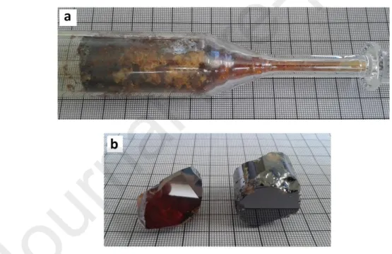
The crystal growth step was carried out using the Bridgman-Stockbarger method (vertical tube furnace manufactured by Cyberstar Inc.). A vacuum sealed quartz ampoule containing the previously synthesized AgGaGeS4 polycrystals (120 g) was used and a single-crystal seed, oriented along (001) direction, was placed at the ampoule's bottom. The ratio between starting elements and the ampoule volume was optimized to moderate stoichiometry deviation during the crystallization process due to GeS2 vaporization. The free ampoule volume above the growing crystal was about 36 cm3. The ampoule was then translated in a 12°C.cm-1 thermal gradient at the rate of 0.4 mm.h-1. At the end, the temperature was decreased to room temperature at 20°C.h-1. Finally, the ampoule was broken in order to get the brown/orange single crystals (Figure 1).
Figure 1 - Growth ampoule containing an as-grown ingot after the Bridgman process (a) and extracted single crystals (b).
2.2. SEM/EDS Characterization
An as-grown single crystal was cut to carry out homogeneity characterizations. Before cutting, the crystal was coated with an epoxy resin in order to facilitate the cutting process and prevent cracks formation. Samples were then polished and the crystal (Figure 2) was placed on a sample holder to perform SEM/EDS characterizations
4
Figure 2 - Picture of the polished crystal used for the chemical mapping
The SEM/EDS method was used to achieve a mapping of the chemical composition of the sample. Such method allows measurements on field size limited to 2x2 mm² maximum, due to limited scan electron beam deflection amplitude. For larger field, as required for the present sample sizing 26x20 mm2, instead of moving the electron beam on the sample surface, the electron beam was fixed and the sample was translated in order to perform an EDS analysis on the whole crystal.
First spectral mapping characterizations (acquisition of an EDS spectrum on each analysis pixel of the map) were performed using a ZEISS DSM962 SEM. The analyses were carried out with a low step stage acquisition (550 µm) on a matrix of 41x50 pixels to cover the whole sample. On each pixel, an EDS spectrum was acquired at 20 kV during 2 s and quantified with standardless method.
In order to determine with a higher precision the chemical composition of the single crystal, other quantitative EDS characterizations with reference samples were realized. These analyses were performed at 15 kV with a spot area of 800x800 µm2, instead of a local point. FeS2, GaP, pure Ge and Ag were used as reference samples for sulfur, gallium, germanium and silver respectively. The sample was divided into two zones (top and bottom), in which several spectra were extracted for each zone from the spectral map for statistical comparison. Finally, a finer view of the chemical homogeneity of the sample was obtained using a ZEISS Merlin SEM (number of matrix pixels in the field = 117x129). A higher resolution with a spot zone of 200x200 µm2 was used. The analyses were performed at 15 kV. The scanning was set in order to get a quantitative measurement on each pixel, using previously cited references samples. The acquisition time was increased to 10 s for each spectrum.
2.3 Thermal annealing treatments
Thermal annealing experiments were performed in order to improve the quality of the as-grown crystals. Annealing was performed under static vacuum (the principle is described in
5
[52]). AgGaGeS4 single crystals and polycrystalline powder (grinded AgGaGeS4) were introduced in the annealing ampoule which was then closed and evacuated. Temperature was raised from room temperature to 600 °C at 3 °C.min-1. Annealing was carried out for 500 h at 600 °C. After this step, temperature was cooled down to room temperature at 0.5 °C.min-1 and the crystal was recovered.
2.4. Optical characterizations
Optical transmission of annealed samples was determined using a Cary 6000 (Varian Inc.) spectrometer for the visible and near-infrared range (0.4-1.7 µm) and a Nicolet 5700 FT- IR spectrometer in the 1.6-14 µm range. Samples were cut and oriented along φ=0° and Ɵ=58 ° for further use in sum frequency generation experiments and polished. Fresnel losses at the air/crystal interfaces were taken into account using Sellmeier equations for the refractive indexes provided by Das et al [53]. In addition, the optical transmission was measured at 1.064 µm using a Nd:YAG laser and at 2.05 µm using a thulium doped fiber CW laser (20 kHz, 100-400 ns, peak power 1 kW [54]) for comparison.
Then, an optical method was used in order to determine the presence of defects or inhomogeneity in the AgGaGeS4 single crystal. The analyses were performed on a sample extracted from the single crystal used for the previous SEM/EDS analysis. A Tm laser emitting at 2 µm was used as a laser source and placed in front of the crystal sample. An infrared camera was placed behind the crystal to analyze the laser beam shape after passing through the crystal.
3. Results and discussion
3.1. SEM/EDS characterizations
The first chemical maps were performed in order to obtain a quick view of the chemical homogeneity of the sample using a ZEISS DSM962 SEM. The results of this qualitative analysis outlined chemical inhomogeneity in the crystal (Figure 3). First, on silver and gallium maps, one can see a color change from blue/green to yellow/red from the bottom to the top of the sample. In opposite, on the same direction, one can see a color change from red/yellow to green/blue on sulfur and germanium maps. This clearly indicates that the phase is depleted in germanium and sulfur and enriched in gallium and silver during the solidification process. Thus, this experiment highlighted a continuous composition change during the crystal growth process leading to inhomogeneity in the final crystal. Furthermore, on the different chemical maps, another kind of inhomogeneity appears as “spots” on the entire sample surface. The origin of these spots was hard to determine according to the scanning SEM resolution and required another chemical map with a higher resolution. This was then performed with quantitative analysis and presented in the following part.
6
Figure 3 – SEM chemical maps with low resolution showing the variation of chemical content for Ag, Ga, Ge and S elements, in weight percentage.
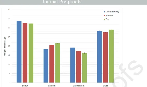
However, to confirm these qualitative results and quantify the observed chemical variations, a quantitative analysis was first performed with the reference samples. Thus, composition on the top and bottom zones of the crystal were determined (Figure 4). First, the sum of mass percentage of each elements is around one hundred percent (and standard deviation is low) which confirmed the measurement's reliability. Then, crystal's bottom appears to be gallium rich and silver, germanium and sulfur poor with mass percentages which are respectively 20.7% (Ga), 27.7% (Ag), 17.4% (Ge) and 32.8% (S) comparing to the stoichiometric composition: 18.4% (Ga), 28.5% (Ag), 19.2% (Ge) and 33.9% (S) respectively. Otherwise, crystal's top appears to be gallium and silver rich but germanium and sulfur poor with mass percentages which are respectively 21.7%, 29%, 16.3% and 32.5%. On average, calculated chemical formulas from the chemical analysis for crystal’s bottom and top are respectively Ag1.00Ga1.10Ge0.90S3.95. and Ag1.00Ga1.10Ge0.80S3.75 taking into account the neutrality rule.
7
Figure 4 - Concentration for each element in w% (Ag, Ga, Ge, S) in the bottom and top zones of the single crystal compared to stoichiometry; standard deviation shown on the bars is an
experimental deviation on six experimental measurements indicating the local chemical homogeneity of the area.
These results confirm the trend observed in the previous experiment, with an increase of gallium and silver concentrations in the crystal along the growth direction and a decrease of the germanium and sulfur contents during the growth process. Otherwise, one can see that germanium and sulfur concentrations are below the stoichiometric point on the entire sample. This is due to the volatility of GeS2 whose influence was enlightened by several authors [41,55]. Indeed, AgGaGeS4 decomposes at high temperature to form AgGaS2 and GeS2 phases. GeS2 vapor pressure increases quickly above 700°C and is about 0.7 bar around the melting point temperature of AgGaGeS4. Thus, this vaporization leads to a deviation in the melt with germanium and sulfur depletion.
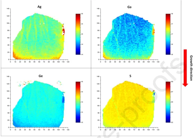
Furthermore, in order to better characterize the local inhomogeneity observed in the first map, another experiment was performed on the Merlin SEM where higher resolution with a spot zone of 200x200 µm2 can be used. Compared to the first one, these new experimental conditions were set in order to get a quantitative measurement on each pixel, using reference samples. The sum of at% for each element was close to 100 % showing the reliability of the measurements. Results of this mapping are shown on Figure 5. First, the same trend as the one obtained in the first mapping is observed, with germanium and sulfur depletions and enrichment in gallium and silver along the solidification direction. This experiment confirmed composition gradients inside the crystal and the deviation from the AgGaGeS4 desired composition.
In addition to the GeS2 volatility, this inhomogeneity comes from chemical instability at the crystallization front. Indeed, in the Bridgman-Stockbarger process, the thermal profile, hotter in the upper part of the furnace, does not lead to efficient convection into the melt. Then, homogenization is also not so efficient.
8
Figure 5 - High resolution map showing the variation of chemical content for Ag, Ga, Ge and S elements, in at%.
Otherwise, with the better scanning resolution, the previously observed “spots” look like “trails” (Figure 5). According to EDS mapping, the observed trails appears poor in GeS2 and are the result of
the decomposition of the liquid at its surface following the chemical reaction: 𝐴𝑔𝐺𝑎𝐺𝑒𝑆4(𝑙) → 𝐴𝑔𝐺𝑎𝑆2(𝑙)+ 𝐺𝑒𝑆2(𝑔)
We can propose the mechanism: on the surface, GeS2 is vaporized and the liquid is locally enriched in
AgGaS2. The higher density of this component makes it sink in the melt as liquid trails. Otherwise,
according to Olekseyuk and al.’s phase diagram [41], the liquidus temperature rises when AgGaS2
concentration increases. So, when it sinks passing through less hot layers (according to the Bridgman process principle) the AgGaS2 rich liquid trails solidify before the rest of the liquid. In parallel, during
the growth, average AgGaS2 concentration increases as well as crystallization temperature that
reduces trails formation and increases solid homogeneity at the top of the ingot as observed on EDS mapping. CFD simulations could help to confirm such a mechanism.
This kind of solute trails which are parallel to the growth direction were observed in other compounds such as ZnGeP2 [26,27]. In some cases, concavity of the crystallization front is also responsible of solute trails formation in the center of the crystals because the growth starts from the edges and excess compounds are rejected to the center of the crucible. Thus, three parameters are responsible for the solute trails formations: (i) lack of melt homogeneity, (ii) GeS2 volatility, (iii) concavity of the solidification front. In order to improve the quality of the grown crystals, it is necessary to control these parameters. First, to increase melt homogeneity, it has be shown that Accelerated Crucible Rotation Technique (ACRT) [56,57] is
9
an interesting solution. This method allows forcing convection by rotation acceleration cycles improving chemical homogenization and allowing controlling the solid/liquid interface shape by thermal homogenization. We simulated ACRT impact on melt homogeneity [58]. The results show that choosing a good set of ACRT parameters, the convection is obviously increased. Simulations of impact on thermal gradient are under progress as well as the trails formation.
Otherwise, it has been shown that germanium and sulfur were below stoichiometry in the crystal. This lack due to germanium sulfide volatility could be limited by adding a controlled excess of these elements.
3.2 Thermal annealing treatments
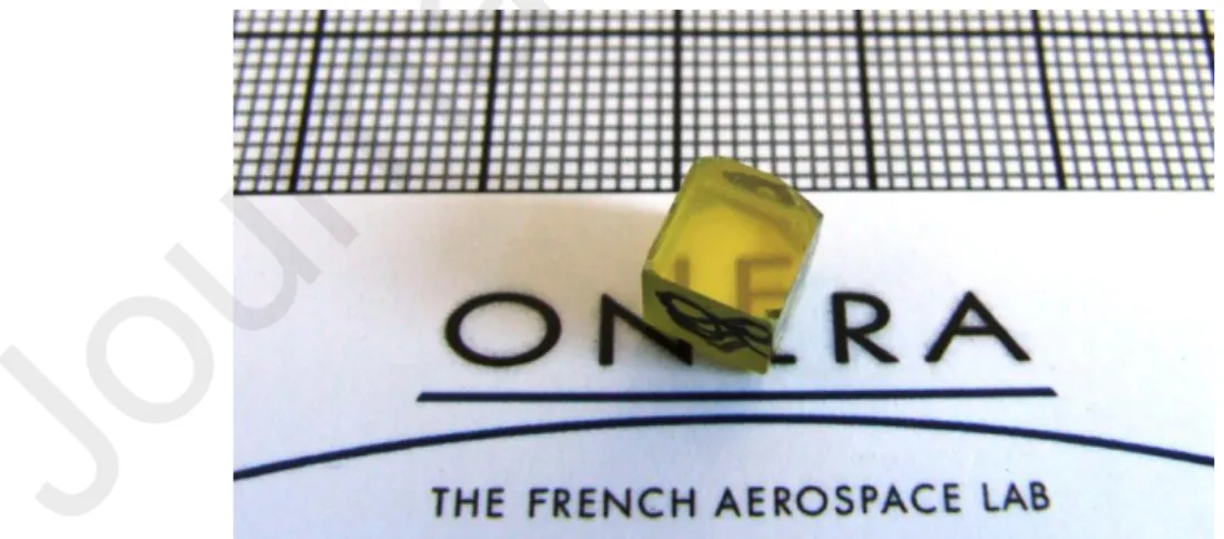
In previous part, crystal’s inhomogeneities were outlined and solutions to improve growth process and crystal quality were presented. However, another way to improve crystal quality is to perform thermal annealing treatments post-growth process [25,52,59]. In the present work, annealing was performed under static vacuum with addition of polycrystalline powder because of volatility of GeS2. Indeed, as previously shown [42,60], volatility of GeS2 can lead to stoichiometry deviation in the melt which increases the final optical absorption coefficient of the crystal. In consequence, annealing under vacuum would increase GeS2 depletion and deteriorate crystal quality. This was recently confirmed by Huang et al. [50] experiments showing that above 500°C (550°C to 700°C), annealing in vacuum drastically reduced transmittance of annealed AgGaGeS4 wafers. Thus, AgGaGeS4 powder was introduced in order to saturate the atmosphere in volatiles as GeS2 and so to limit vaporization from single crystals. After 500 h at 600 °C, crystal color changed from brown/orange to yellow as shown on the Figure 6. Measurements of absorption coefficient before and after annealing presented in [42] showed blue shift of the cut-off wavelength, from 0.49 µm to 0.45 µm, before and after annealing respectively which explains the color change.
Figure 6 - Picture of the oriented crystal used for the optical characterizations
3.3. Optical Characterizations
Real composition of the ingot is not easy to measure with a good accuracy on the entire volume. This is why we outlined chemistry deviations by optical absorption data as well as results of laser beam
10
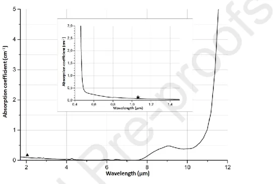
experiment. The aim was to evaluate if the annealing step was efficient to suppress the chemical inhomogeneities observed in the chemical mapping experiments and to provide a crystal suitable for optical applications. First, the optical transmission of the annealed crystal in the middle infrared range was measured (see Figure 7). The absorption coefficient was around 0.1 cm-1 from 1 to 8 µm using a FTIR spectrometer. Moreover, more accurate laser measurements at 1.064 µm and 2.05 µm resulted in 0.12±0.02 and 0.17±0.08 cm-1 absorption coefficients respectively. These data indicate that the crystal is suitable in term of optical absorption for further optical experiments.
Figure 7 – Optical absorption in the mid-IR range of cut and polished sample (thickness: 6 mm): with a FTIR spectrophotometer (solid curve); and with a Nd: YAG laser (star) and a
thulium doped fiber laser (triangle).
Then, homogeneity of the crystal was evaluated using an optical method. The shape of a laser beam was analyzed after going through the crystal. The initial shape of the laser beam is shown on the Figure 8-a. One can see that the beam is circular, with a 5 mm diameter and a Gaussian profile. The size of the beam is larger than the crystal which allows fully illuminating the sample. After passing through the crystal, the shape is slightly disturbed. Fringes due to inhomogeneous optical properties appear as seen on the Figure 8-b,c. These fringes are linked to the chemical inhomogeneity in the crystal as observed in the previous SEM/EDS analysis. Thus, the annealing post-treatment do not fully restore crystal stoichiometry. Further experiments must be carried out with GeS2 excess in order to improve the annealing process. At least, the laser beam was focused using a converging lens in order to locally scan the different parts of the crystal. Figure 8-a’ shows the shape of the focused laser beam which is circular with a 1.6 mm diameter (on the IR camera). By scanning the different parts of the crystal, one can see that the beam can pass through the crystal without (Figure 8-b’) or with (Figure 8-c’) distortion.
11
Figure 8 – Spatial characterization of a 2.05 µm laser: with a non-focused beam [(a) = before sample; (b) and (c) = after sample depending on the polarization]; with a focused beam [(a’)
= before sample; (b') and (c') after sample]. Sample thickness = 6 mm.
One relevant application of these new crystals can be the control of ultrafast lasers in the middle infrared spectral range. In fs regime in the middle infrared range, the AgGaGeS4 can efficiently replace lithium niobate based compounds whose transparency limits it uses beyond 5 µm. First tests developed at the LOB Laboratory (Ecole Polytechnique, France) are promising and showed conversion efficiency at 5.9 µm four times higher for AgGaGeS4 crystal than for MgO:PPLN with better beam stability. Furthers characterizations are still in progress and results will be published elsewhere.
4. Conclusion
The crystal quality of an AgGaGeS4 single crystal grown by the Bridgman-Stockbarger method was studied. SEM, combined with EDS, was first used to perform a chemical mapping of a large single crystal surface. It has shown an increase of gallium and silver concentration and a decrease of germanium and sulfur content along the crystal growth direction. GeS2 volatility, lack of melt homogenization and instability of the crystallization front are responsible of these issues. However, EDS mapping showed trails in the crystal whose origin is a mixing between thermodynamics and kinetics phenomena. That direct observation of trails is particularly interesting for computational fluid dynamics (CFD) simulations giving target for such calculations. Simulations are currently in progress to understand the trails formation mechanism.
Then, that was confirmed by an optical method consisting of an analysis of a laser beam shape after going through the sample.
Now, knowing the nature of the defects, better crystals can be obtained. Particularly by forcing the convection in the crucible and adding an excess of germanium sulfide which open the path to new applications in the MIR range.
12
Acknowledgements
The authors would like to thank V. Kemlin, A. Bonvaler and M. Joffre from LOB at Ecole Polytechnique (France) for optical testing of AgGaGeS4 crystal.
References
J. Rame : Conceptualization, investigation J. Petit : methodology, funding acquisition D. Boivin : validation, ressources
N. Horezan : investigation JM Melkonian : investigation A. Godard : project administration B. Viana : validation, supervision
Highlights :
A precise, large crystal area, high resolution, chemical analysis helps to understand volume defects origins.
Bridgman grown AgGaGeS4 shows chemical trails
Depletion of GeS2 is responsible of chemical gradients in AgGaGeS4
[1]D. M. Bubb, J. S. Horwitz, M. R. Papantonakis and R. F. Haglund, "Resonant infrared pulsed laser deposition of polymers using a picosecond tunable free-electron laser," Summaries of Papers Presented at the Lasers and
Electro-Optics. CLEO '02. Technical Diges, Long Beach, CA, USA, 2002, pp. 94-95 vol.1
[2] A. Godard, “Infrared (2–12 μm) solid-state laser sources: a review,” Comptes Rendus Phys. 8, (2007) 1100– 1128
[3] V. Petrov, “Parametric down-conversion devices: The coverage of the mid-infrared spectral range by solid-state laser sources,” Opt. Mater. 34 (2012) 536–554.
[4] G. Overton, “Photonics Applied - Defense:: IR countermeasures aim for safer flights,” Laser Focus World, 47 (2011).
[5] J. Hecht, “Photonic Frontiers: Laser Countermeasures: Scaling down mid-IR laser countermeasures for smaller aircraft,” Laser Focus World, 50 (2014) 31–38.
[6] T. Day, M. Pushkarsky, D. Caffey, K. Cecchetti, R. Arp, A. Whitmore, M. Henson, E. B. Takeuchi, “Quantum cascade lasers for defense and security,” Proc of SPIE Technologies for optical countermeasures X ; High power laser, 8898 (2013). 889802.
[7] K. Regelskis, J. Želudevičius, N. Gavrilin, and G. Račiukaitis, “Efficient second-harmonic generation of a broadband radiation by control of the temperature distribution along a nonlinear crystal,” Opt. Express 20 (2012) 28544.
13
[8] G. Bhar and R. Smith, “Silver thiogallate (AgGaS 2 ) - Part II: Linear optical properties,” IEEE J. Quantum Electron. 10 (1974) 546–550.
[9] P. Canarelli, Z. Benko, A. K. Hielscher, R. F. Curl, and F. K. Tittel, “Measurement of nonlinear coefficient and phase matching characteristics of AgGaS2”, IEEE J. Quantum Electron. 28 (1992) 52–55.
[10] G. Boyd, H. Kasper, J. McFee, “Linear and nonlinear optical properties of AgGaS2, CuGaS2, and CuInS2, and theory of the wedge technique for the measurement of nonlinear coefficients”, IEEE J. Quantum Elect. 7 (1971), 563-573.
[11] G. C. Bhar, S. Das, D. K. Ghosh, and L. K. Samanta, “Phasematching of infrared nonlinear laser devices using AgGaS2”, IEEE J. Quantum Electron. 24 (1988) 1492–1494.
[12] T. Dahinten, U. Plodereder, A. Seilmeier, K. L. Vodopyanov, K. R. Allakhverdiev, and Z. A. Ibragimov, “Infrared pulses of 1 picosecond duration tunable between 4 mu m and 18 mu m,” IEEE J. Quantum Electron. 29 (1993) 2245–2250.
[13] K. Kato, “High-power difference-frequency generation at 5-11 µm in AgGaS2”, IEEE J. Quantum Electron., 20 (1984) 698–699.
[14] P. Kupecek, C. Schwartz, and D. Chemla, “Silver thiogallate (AgGaS 2 ) - Part 1: Nonlinear optical properties,” IEEE J. Quantum Electron. 10 (1974) 540–545.
[15] R. C. Eckardt, Y. X. Fan, R. L. Byer, R. K. Route, R. S. Feigelson, J. van der Laan, “Efficient second harmonic generation of 10‐μm radiation in AgGaSe 2,” Appl. Phys. Lett., 47 (1985) 786–788.
[16] G. Anandha Babu, R. Subramaniyan, N. Karunagaran, R. Perumal Ramasamy, P. S. Ganesamoorthy, P. K. Gupta, “Growth improvement of AgGaSe2 single crystal using the vertical Bridgman technique with steady ampoule rotation and its characterization,” J. Cryst. Growth, 338 (2012) 42–46.
[17] J.-J. Zondy, “Experimental investigation of single and twin AgGaSe2 crystals for CW 10.2 μm SHG,” Opt. Commun. 119 (1995) 320–326.
[18] N.-H. Kim, D. H. Shin, and R. S. Feigelson, “Heat treatment studies on silver gallium diselenide (AgGaSe2) crystals,” Mater. Sci. Eng. B, 38 (1996) 229–235.
[19] K.-M. Nigge, F. P. Baumgartner,E. Bucher, “CVT-growth of AgGaSe2 single crystals: Electrical and photoluminescence properties,” Sol. Energy Mater. Sol. Cells, 43 (1996) 335–343.
[20] R. K. Route, R. S. Feigelson, R. J. Raymakers, M. M. Choy, “Elimination of optical scattering defects in AgGaS2 and AgGaSe2,” J. Cryst. Growth, 33 (1976) 239–245.
[21] W. Z. Shen, S. C. Shen, Y. Chang, W. G. Tang, G. C. Chen, L. Yang, “Identification of near-infrared absorption bands in AgGaSe2,” Infrared Phys. Technol., 38 (1997) 113–116.
[22] B. J. Zhao, S. F. Zhu, S. S. Fu, Q. F. Li, Y. R. Jin, Z. H. Li, “New way of preparation and orientation processing of AgGaSe2 crystals,” Mater. Res. Bull., 35 (2000) 1525–1532.
[23] S. Zhu, B. Zhao, J. Liu, Z. Li, and W. Li, “Heat treatment and its effects on the optical quality of AgGaSe2 single crystals,” Mater. Chem. Phys., 50 (1997) 94–97.
[24] J. Petit, S. A. Said Hassani, P. Galtier, A. Godard, M. Raybaut, M. Lefebvre, “Progress in ZnGeP 2 and AgGaS 2 crystal growth: first results on difference-frequency generation and optical parametric oscillation”, Proc of SPIE, 7487 (2009) 748701.
[25] Z. Lei, C. Zhu, C. Xu, B. Yao, C. Yang, “Growth of crack-free ZnGeP2 large single crystals for high-power mid-infrared OPO applications,” J. Cryst. Growth, 389 (2014) 23–29.
[26] G. A. Verozubova, A. O. Okunev, A. I. Gribenyukov, A. Y. Trofimiv, E. M. Trukhanov, A. V. Kolesnikov, “Growth and defect structure of ZnGeP2 crystals,” J. Cryst. Growth, 312 (2010) 1122–1126.
[27] G. A. Verozubova, A. I. Gribenyukov, V. V. Korotkova, A. W. Vere, C. J. Flynn, “ZnGeP2 growth: melt non-stoichiometry and defect substructure,” J. Cryst. Growth, 237–239 (2002) 2000–2004.
[28] G. A. Verozubova, A. I. Gribenyukov, V. V. Korotkova, M. P. Ruzaikin, “ZnGeP2 synthesis and growth from melt,” Mater. Sci. Eng. B, 48 (1997) 191–197.
[29] J. Cheng, S. Zhu, B. Zhao, B. Chen, Z. He, Q. Fan, T. Xu, “Synthesis and growth of ZnGeP2 crystals: Prevention of non-stoichiometry,” J. Cryst. Growth, 362 (2013) 125–129.
[30] P. G. Schunemann, K. L. Schepler, P. A. Budni, “Nonlinear Frequency Conversion Performance of AgGaSe2, ZnGeP2, and CdGeAs2,” MRS Bull., 23 (1998) 45–49.
[31] W. Huang, Z. He, S. Zhu, B. Zhao, B. Chen, S. Zhu, “Polycrystal Synthesis, Crystal Growth, Structure, and Optical Properties of AgGaGenS2(n+1) (n = 2, 3, 4, and 5) Single Crystals for Mid-IR Laser Applications.”, Inorg. Chem. 58 (2019) 5865-5874.
[32] V. Badikov, A. Tyulyupa, G. Shevyrdyaeva, S. G. Sheina, « Solid solutions in the AgGaS2-GeS2 and AgGaSe2-GeSe2 systems », Inorg. Mater. 27 (1991) 177-180.
[33] P. G. Schunemann, K. T. Zawilski, T. M. Pollak, « Horizontal gradeint freeze growth of AgGaGeS4 and AgGaGeSe12 », Journal of Crystal Growth, 287 (2006) 248-251.
14
[34] Y. M. Andreev, P. P. Geiko, V. V. Badikov, G. C. Bhar, S. Das, A. K. Chaudhury, « Nonlinear optical properties of defect tetrahedral crystals HgGaS4 and AgGaGeS4 and mixed chalcopyrite crystal Cd(0.4)Hg(0.6)Ga2S4 », Nonl. Opt. 29 (2002) 19-27.
[35] V. Petrov, V. Badikov, G. Shevyrdyaeva, V. Panyutin, V. Chizhikov, “Phase-matching properties and optical parametric amplification in single crystals of AgGaGeS4,” Opt. Mater., 26 (2004) 217–222.
[36] K. Miyata, V. Petrov, K. Kato, “Phase-matching properties for AgGaGeS4” Appl Opt., 46 (2007) 6848–6848. [37] Y. Ni, H. Wu, Z. Wang, M. Mao, G. Cheng, H. Fei, “Synthesis and growth of nonlinear infrared crystal material AgGeGaS4 via a new reaction route,” J. Cryst. Growth, 311 (2009) 1404–1406.
[38] O. M. Yurchenko, I. D. Olekseyuk, O. V. Parasyuk, and V. Z. Pankevich, “Single crystal growth and properties of AgGaGeS4,” J. Cryst. Growth, 275 (2005) 1983–1985.
[39] M. V. Shevchuk , V. V. Atuchin, A. V. Kityk, A. O. Fedorchuk, Y. E. Romanyuk, S. Catus, O. M. Yurchenko, O. V. Parasyuk, “Single crystal preparation and properties of the AgGaGeS4–AgGaGe3Se8 solid solution,” J. Cryst. Growth, 318 (2011) 708–712.
[40] H. Wu, Y. Ni, C. Lin, M. Mao, G. Cheng, and Z. Wang, “Growth of large size AgGaGeS4 crystal for infrared conversion,” Front. Optoelectron. China, 4 (2011) 137–140.
[41] I. Olekseyuk, G. Gorgut, M. Shevtchuk, “Phase equilibria in the AgGaS2-GeS2 systems”, Polish J. Chem. 76 (2002) 915-919.
[42] J. Rame, B. Viana, Q. Clement, J. M. Melkonian, and J. Petit, “Control of Melt Decomposition for the Growth of High Quality AgGaGeS 4 Single Crystals for Mid-IR Laser Applications,” Cryst. Growth Des., 14 (2014) 5554–5560.
[43] C. Huang, M. Mao, H. Wu, J. Ma, « Pressure-Assisted Method for the Preparations of High-Quality AgGaS2 and AgGaGeS4 Crystals for Mid-Infrared Laser Applications”, Inorg. Chem., 57 (2018) 14866-14871
[44] W. Huang, Z. He, B. Zhao, S. Zhu, B. Chen, « Crystal growth structure and optical properties of new quaternary chalcogenide nonlinear optical crystal AgGaGeS4 », Journal of Alloys and Compounds 796 (2019) 138-145
[45] A. Sodeika, Z. Silevičius, Z. Januškevičius, A. Sakalas, “The Influence of Intrinsic Defects on the Electrical Properties of Single Crystals of CdSiP2 and ZnGeP2,” Phys. Status Solidi A, 69 (1982) 491–495.
[46] L. E. Halliburton, G. J. Edwards, M. P. Scripsick, M. H. Rakowsky, P. G. Schunemann, T. M. Pollak, “Electron-nuclear double resonance of the zinc vacancy in ZnGeP2,” Appl. Phys. Lett., 66 (1995) 2670, 1995.
[47] Y. Shimony, R. Fledman, I. Dahan, and G. Kimmel, “Anti-phase domain boundaries in ZnGeP2 (ZGP),” Opt. Mater., 16 (2001) 119–123.
[48] W. Huang, B. Zhao, S. Zhu, Z. He, B. Chen, Y. Pu, L. Lin, Z. Zhao, Y. Zhong, « Synthesis of AgGaGeS4
polycrystalline materials by vapor transporting and mechanical oscillation method », Journal of Crystal Growth 468 (2017) 469-472
[49] J. Wu, W. Huang, H-G. Liu, Z. He, B. Chen, S. Zhu, B. Zhao, Y. Lei, X. Zhou, « Investigation of the thermal properties and crystal graowth of the nonlinear optical crystals AgGaS2 and AgGaGeS4 », Crystal Growth and Design XX (2020) XXXX
[50] W. Huang, Z. He, B. Zhao, S. Zhu, B. Chen, Y. Wu, « Effect of thermal annealing treatment and defect analysis on AgGaGeS4 single crystals », Inorg. Chem 58 (2019) 10846-10855
[51] W. Huang, Z. He, S. Zhu, B. Zhao, B. Chen, S. Zhu, “Polycrystal Synthesis, Crystal Growth, Structure, and Optical Properties of AgGaGenS2(n+1) (n = 2, 3, 4, and 5) Single Crystals for Mid-IR Laser Applications.”, Inorg. Chem. 58 (2019) 5865-5874.
[52] J. Petit, M. Bejet, J-C. Daux, « Highly transparent AgGaS2 single crystals, a compound for mid IR laser sources, using a combined static/dynamic vacuum annealing method », Materials Chemistry and Physics 119 (2010) 1-3
[53] S. Das, C. Ghosh, S. Gangopadhyay, Y. M. Andreev, and V. V. Badikov, “AgGaGeS4 Crystals for Nonlinear Laser Device Applications,” Jpn. J. Appl. Phys., 45 (2006) 5795–5797.
[54] E. M. D. Lucas, G. Canat, L. Lombard, Y. Jaouën, and S. Bordais, “Pulsed kW-peak power and integrated all fiber MOPA single-frequency source at 2050nm,” in Proc. SPIE 9135, Laser Sources and Applications II, Brussels, Belgium, 9135 (2014) 91350M–91350M–7.
[55] R. E. Nikolaev and I. G. Vasilyeva, “A new way of phase identification, of AgGaGeS4,nGeS2 crystals,” J. Solid State Chem., 203 (2013) 340–344.
[56] L. Juncheng, “ACRT forced convection and its effects on solute segregation and heat and mass transfer during single crystal growth,” Cryst. Res. Technol., 43 (2008) 396–408.
[57] Y.-B. Xu and S.-J. Fan, “Accelerated crucible rotation technique: Bridgman growth of Li2B4O7 single crystal and simulation of the flows in the crucible,” J. Cryst. Growth, 133 (1993) 95–100.
15
[58] V. Tabouret, J. Petit, B. Viana, « Melt homogenization improvement during the Bridgman crystal growth optimizing the rotation profile », Proceeding of COMSOL Conference (October 2016) Munich, Allemagne [59] K. T. Zawilski, P. G. Schunemann, S. D. Setzler, T. M. Pollak, “Large aperture single crystal ZnGeP2 for high-energy applications”, Journal of Crystal Growth, 310 (2008) 1891–1896
[60] I. G. Vasilyeva and R. E. Nikolaev, “Saturated vapor pressure over AgGaGeS4 crystals,” Inorg. Mater. 42 (2006) 1299–1301.


![Figure 8 – Spatial characterization of a 2.05 µm laser: with a non-focused beam [(a) = before sample; (b) and (c) = after sample depending on the polarization]; with a focused beam [(a’)](https://thumb-eu.123doks.com/thumbv2/123doknet/7766974.256132/13.892.252.757.111.428/figure-spatial-characterization-focused-sample-depending-polarization-focused.webp)
