To link to this article: DOI: 10.1063/1.3616147
URL :
http://dx.doi.org/10.1063/1.3616147
This is an author-deposited version published in:
http://oatao.univ-toulouse.fr/
Eprints ID: 5666
To cite this version:
Mahfoud, Tarik and Molnar , Gabor and Cobo , Saioa and Salmon, Lionel
and Thibault, Christophe and Vieu, Christophe and Demont , Philippe and
Bousseksou, Azzedine Electrical properties and non-volatile memory
effect of the [Fe(HB(pz)3)2] spin crossover complex integrated in a
microelectrode device. (2011) Applied Physics Letters , vol. 99 (n° 5). pp.
053307(1)-053307(3). ISSN 0003-6951
O
pen
A
rchive
T
oulouse
A
rchive
O
uverte (
OATAO
)
OATAO is an open access repository that collects the work of Toulouse researchers
and makes it freely available over the web where possible.
Any correspondence concerning this service should be sent to the repository
administrator:
staff-oatao@listes.diff.inp-toulouse.fr
Electrical properties and non-volatile memory effect of the [Fe(HB(pz)
3)
2]
spin crossover complex integrated in a microelectrode device
Tarik Mahfoud,1Ga´bor Molna´r,1Saioa Cobo,1Lionel Salmon,1Christophe Thibault,2 Christophe Vieu,2Philippe Demont,3and Azzedine Bousseksou1,a)1LCC, CNRS & Universite´ de Toulouse, UPS, INPT, 205 route de Narbonne, 31077 Toulouse, France 2LAAS-CNRS, Universite´ de Toulouse, UPS, INSA, IAES, 7 avenue du colonel Roche, 31077 Toulouse, France 3LPP-CIRIMAT, CNRS &, Universite´ de Toulouse III, 118 route de Narbonne, 31062 Toulouse, France
We report on the deposition of thin films of the [Fe(HB(pz)3)2] (pz ¼ pyrazolyl) molecular spin
crossover complex by thermal evaporation. By means of impedance measurements and Raman microspectroscopy, we show that the films maintain the structure and properties of the bulk material. The conductivity of the films decreases by ca. 2 orders of magnitude when the freshly deposited compound goes through a first (irreversible) thermal phase change above ca. 380 K. This property can be exploited as a non-volatile (read-only) memory effect.
[doi:10.1063/1.3616147]
Certain 3d4-3d7 transition metal complexes are known to display a molecular bistability of their high-spin (HS) and low-spin (LS) electron configurations.1 The electronic ground state of these complexes may be reversibly inter-changed by various stimuli such as temperature, pressure, magnetic field, light irradiation, etc. This so-called spin-crossover (SCO) phenomenon is of growing importance in the area of functional materials with possible applications in sensor, display, information storage, and photonic devices.2 The bistability of the 3d electron configurations implies im-portant changes of material properties including magnetic, structural, optical, and electrical properties. Up to now, this latter property has received much less attention – certainly due to the highly insulating nature of these molecular materi-als.3–9 For this reason, we have proposed to use dielectric spectroscopy measurements and we have shown that changes in the real part of the dielectric permittivity can be conven-iently used to follow the molecular spin state change (in the quasi-static frequency range).3 Based on this property, we have constructed a non-volatile memory device composed of micro-capacitances wherein the information is stored in the high- and low-capacitance states.10Several efforts have been made also to combine the SCO property with conductivity within the same material.11,12 On the other hand, in a few cases, such as for the compound [Fe(HB(pz)3)2],13the
elec-trical conductivity of the material and the conductivity change upon SCO are sufficiently high in itself to consider this property for practical uses even without the introduction of additional “conductive bricks.”
The compound [Fe(HB(pz)3)2] is one of the most singular
examples of the family of SCO complexes.13,14 In this ther-mochromic molecule, the Fe(II) ions undergo a thermally induced spin crossover between their 1A1 (LS) and5T2(HS)
electronic configurations in the 300–450 K temperature range. Interestingly, the thermal spin transition curve recorded during the first heating differs drastically from the successive thermal cycles. It reveals irreversible changes in the magnetic and op-tical properties in the material, which was first attributed to a
self-grinding process.15 More recently, we have shown that the irreversible transformation has a crystallographic origin and should be associated with a transformation between a metastable tetragonal and the stable monoclinic forms.13 In the course of this study, interesting and unexpected electrical properties of [Fe(HB(pz)3)2] have been also uncovered. In
particular, we have shown that the conductivity changes by 3–4 orders of magnitude when the material passes through the first (irreversible) transition. Since this compound can be sub-limated at high temperatures, it should be possible to integrate it into an electronic device. In this letter, we report on the deposition and electrical properties of thin films of [Fe(HB(pz)3)2]. We show that the films maintain the physical
properties of the bulk material and exhibit an irreversible phase change associated with a conductivity drop that can be exploited as a read-only memory (ROM) effect.
The [Fe(HB(pz)3)2] complex was synthesized as
described earlier in Ref.13. Thin films of ca. 200 nm thick-ness of the [Fe(HB(pz)3)2] complex were deposited on gold
interdigitated microelectrodes (10 lm width, 10 lm gap, and 120 nm thickness on a Si wafer covered by a 190 nm SiO2
insulating layer) by thermal evaporation under secondary vacuum of ca. 10ÿ5mbar. The film thickness was determined
in-situ by means of a quartz crystal microbalance. In order to be sure that the thin films keep the same composition and crystal structure as the bulk [Fe(HB(pz)3)2] powder, we
acquired Raman spectra of both samples. The recorded Raman patterns of [Fe(HB(pz)3)2] were very similar
demon-strating thus that the films preserve the crystalline integrity of the bulk compounds.17
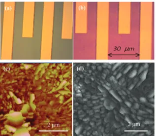
The film quality was characterized by optical micros-copy, atomic force microscopy (AFM), and scanning elec-tron microscopy (SEM) revealing a dense surface covering (Fig.1). The film morphology is granular, and composed of nanocrystals, the size of which varies depending on the film thickness.
For the electrical measurements, the microelectrodes were assembled in a TO-8 (transistor outline) package, while the powder sample was sandwiched between two plate elec-trodes. In order to prevent evaporation of the [Fe(HB(pz)3)2] a)
film at higher temperatures, the devices were encapsulated by a poly-dime´thylsiloxane layer. AC conductivity measure-ments were carried out as a function of frequency (10ÿ2–106
Hz) and temperature (298–410 K) by means of a broadband dielectric spectrometer (Novocontrol) at an applied ac volt-age of 1 Vrms. Frequency sweeps were carried out
isother-mally. The frequency dependence of the real part of the complex conductivity, r0(f), reveals a low- and a
high-fre-quency region at each temperature for the powder and thin film samples as well (Fig. 3). In both cases, the high fre-quency part of the spectrum is characterized by a higher con-ductivity and the critical frequency, fc, which separates the
two regions increases continuously with increasing tempera-ture. The conductivity of the film samples exhibits a more
pronounced frequency dependence, which may indicate a higher degree of disorder.
Figure2 exhibits also the thermal variation of the real part of the complex conductivity (r0) at 10 mHz. During the
first heating sequence, the conductivity is strongly activated up to ca. 350 K, but then it starts to decrease slowly. In the case of the powder sample, r0exhibits an abrupt drop at 415
K, which is not observed for the film sample. Furthermore, the conductivity of the as-prepared film is significantly lower than that of the freshly sublimated powder. These differences between the film and the powder should certainly be traced back to the different electrode configurations and perhaps to the presence of a small amount of monoclinic form in the as-prepared film. On the other hand, the powder and film sam-ples resemble closely in that all successive heating and cool-ing cycles follow a common trace, which differs significantly from the first heating curve, i.e., in both samples there is an irreversible phase change during the first heating (Fig.2). The electrical conductivity (at a given temperature) is always smaller by several orders of magnitude when com-pared to the first heating curve. As explained in Ref.13, the conductivity data can be clearly correlated with the crystallo-graphic and spin state changes in the sample. When the tem-perature is increased for the first time, the conductivity of the sample (LS, tetragonal) increases also, but above ca. 350 K the LS ! HS crossover counterbalances the effect of the thermal activation, which means that the HS form of the compound is less conductive than the LS form. For further increase of the temperature, an irreversible transition occurs towards the thermodynamically stable monoclinic form. This stable phase is significantly more insulating than the “as pre-pared” tetragonal form (at a given temperature).
As far as the charge transport mechanism is considered, in such a low-mobility solid, the conductivity should be asso-ciated by a charge hopping process. These processes can be
FIG. 2. (Color online) Temperature
dependence of the ac conductivity of
[Fe(HB(pz)3)2] for microcrystalline
powder (a) and (c) and thin film samples (b) and (d). (a) and (b) The frequency
dependence of the conductivity at
selected temperatures (first heating
sequence); (c) and (d) the temperature
dependence of r0 recorded at 10 mHz
over two successive thermal cycles. At
this frequency, r0 can be assimilated
with rdc. FIG. 1. (Color online) Bright field optical microscopy images of the
micro-electrodes before (a) and after (b) the deposition of a [Fe(HB(pz)3)2] thin film. AFM (c) and SEM (d) images showing the film morphology.
straightforwardly analyzed within the electric modulus (M*(x) ¼ 1/e*(x)) formalism.16Indeed, the frequency of the M00peak maximum is defined as the dielectric relaxation
fre-quency (xp), and it was found to increase with increasing
temperature in the [Fe(HB(pz)3)2] samples.17The Arrhenius
activation energy of the dielectric relaxation (0.58 eV 6 0.01) was found very close to the activation energy of the conductivity (0.62 6 0.01 eV) during the first heating sequence (below the phase change temperature). The observed dielectric relaxation is therefore due to the electri-cal conduction, and we can associate the observed relaxation frequency with the charge carrier hopping frequency.
The irreversible thermal transition in the conductivity of [Fe(HB(pz)3)2] thin films motivated us to test the idea of
using our device as a non-volatile ROM. The memorization (write) process consists of switching the compound from the as-prepared tetragonal LS form to the monoclinic HS state by heating, either by increasing the temperature of the whole device or by passing a current through the sample (Joule effect). The read operation was performed by sensing the de-vice resistivity at a lower temperature. In these experiments, direct current as a function of an applied dc voltage was measured using a Keithley 6430 source-meter. The tempera-ture of the device was adjusted in the 298–410 K range by means of a custom-modified, electrically shielded, cryostat. For applied voltages up to ca. 3 V, the I-V curves displayed Ohmic characteristics. Figure 3 shows the I-V curves recorded at 295 K before and after heating the device to 408 K (write process). One can observe 1 order of magnitude dif-ference of the current for the same applied voltages. This measurement corresponds thus to a very straightforward room temperature read process.
We carried out another experiment where the electric bias can be an indirect trigger (by Joule effect) for the write process. In this experiment, we fixed the device temperature at 370 K. Then we increased the electric bias from 1 V to 10 V in a step-wise manner. Each bias was applied for ca. 1 min. As shown in Figure3at 1 V, the measured current was about 15 nA. At 2 V, the current flowing through the device was 42 nA at the be-ginning of the experiment, but it dropped to 0.4 nA after 40 s. Further increase of the bias above 2 V was accompanied by a
small increase of the electric current but remarkably, the cur-rent remained in the low conductivity region. Of course the actual value of the “switching bias” depends on the device tem-perature and the time, i.e., at lower temtem-peratures one has to apply either higher bias or wait longer (and vice-versa).
In summary, we have succeeded to deposit thin films of the molecular spin crossover complex [Fe(HB(pz)3)2], and
we have shown that the films preserve the structure and prop-erties of the bulk material. Most importantly, we have shown that the conductivity of the films decreases by ca. 1–2 orders of magnitude (depending on the experimental conditions) when the material goes through the first (irreversible) ther-mal phase change. This property together with the fact that this compound is stable to exposure to light, electromagnetic fields, air, and water can be exploited in ROM type devices where the writing process can be performed by heating the cell and the read out can be achieved at room temperature by simply measuring the resistivity of the device. Further work on the synthesis and characterization of this type of com-pounds should allow tuning the SCO properties and achieve an even more efficient read-write-erase type device based on the hysteresis phenomenon, which accompanies in certain cases the spin crossover.
This work was supported by the project CROSS-NANO-MAT (ANR 2010 BLAN 7161).
1
P. Gu¨tlich et al., Angew. Chem. Int. Ed. 33, 2024 (1994). 2
A. Bousseksou et al.,Chem. Soc. Rev.40, 3313 (2011).
3A. Bousseksou et al.,J. Mater. Chem.13, 2069 (2003).
4S. Bonhommeau et al., Angew. Chem. Int. Ed. 45, 1625 (2006).
5T. Guillon et al.,Phys. Status Solidi A203, 2974 (2006). 6
T. Guillon et al.,J. Phys. Chem. A111, 8223 (2007).
7
S. Shi et al.,Appl. Phys. Lett.95, 043303 (2009). 8
T. Mahfoud et al.,J. Am. Chem. Soc.131, 15049 (2009).
9
F. Prins et al.,Adv. Mater.23, 1545 (2011).
10A. Bousseksou et al., EU patent 1,430,552 (2004).
11S. Dorbes et al.,Chem. Commun.41, 69 (2005).
12K. Takahashi et al.,Inorg. Chem.45, 5739 (2006).
13
L. Salmon et al.,New J. Chem.33, 1283 (2009).
14
G. J. Long et al.,Top. Curr. Chem.233, 91 (2004).
15
F. Grandjean et al.,Inorg. Chem.28, 4406 (1989).
16J. C. Dyre and T. B. Schroder,Rev. Mod. Phys.72, 873 (2000).
17See supplementary material at http://dx.doi.org/10.1063/1.3616147 for
Raman spectra and dielectric relaxation data.
FIG. 3. (Color online) (a) I-V characteristics of the [Fe(HB(pz)3)2] thin film based device recorded at 295 K before and after the write process. (b) Step-wise increase of the applied bias at 370 K revealing the switching (write) process for 2 V applied bias. (Data points are connected to guide the eye.)