HAL Id: tel-01496838
https://pastel.archives-ouvertes.fr/tel-01496838
Submitted on 27 Mar 2017
HAL is a multi-disciplinary open access archive for the deposit and dissemination of sci-entific research documents, whether they are pub-lished or not. The documents may come from teaching and research institutions in France or abroad, or from public or private research centers.
L’archive ouverte pluridisciplinaire HAL, est destinée au dépôt et à la diffusion de documents scientifiques de niveau recherche, publiés ou non, émanant des établissements d’enseignement et de recherche français ou étrangers, des laboratoires publics ou privés.
Silicon Nanowires for Photovoltaics : from the Material
to the Device
Alienor Togonal
To cite this version:
Alienor Togonal. Silicon Nanowires for Photovoltaics : from the Material to the Device. Micro and nanotechnologies/Microelectronics. Université Paris Saclay (COmUE); Nanyang Technological Uni-versity, 2016. English. �NNT : 2016SACLX032�. �tel-01496838�
NNT : 2016SACLX032
T
HESE DE DOCTORAT
DE
L’U
NIVERSITE
P
ARIS
-S
ACLAY
PREPAREE A
L’ECOLE
POLYTECHNIQUE
ECOLE DOCTORALE N° 573
Interfaces : approches interdisciplinaires, fondements, applications et innovation School of Electrical & Electronic Engineering
Spécialité de doctorat: Physique
Par
Mme Aliénor Togonal
Silicon Nanowires for Photovoltaics: from the Material to the Device
Thèse présentée et soutenue à L'Ecole Polytechnique, le 20 Avril 2016 : Composition du Jury :
Mr Zhang Qing Professeur, Nanyang Technological University Président du jury
Mr Wong Kin Shun Terence Professeur Associé, Nanyang Technological University Rapporteur Mr Thierry Gacoin Professeur, Ecole Polytechnique Rapporteur
Mr Professor Ravi Silva Professeur,University of Surrey Rapporteur Mr Pere Roca i Cabarrocas Professeur, Ecole Polytechnique Directeur de thèse Mr Rusli Professeur, Nanyang Technological University Co-directeur de thèse
Silicon Nanowires for Photovoltaics: from
the Material to the Device
ALIENOR SVIETLANA TOGONAL
School of Electrical & Electronic Engineering
A thesis submitted to the Nanyang Technological University
in partial fulfillment of the requirement for the degree of
Doctor of Philosophy
To my sunshine Pierre, my love and faithful travel and underwater buddy To my parents, Stéphane and Catherine Togonal, for their love, endless support
Acknowledgements
Here we are: the completion of 4 years of PhD between France and Singapore... What an adventure! I have so many people to thank that have made this experience so fulfilling and fruitful.
Above all, I would like to thank my two supervisors, Prof RUSLI and Prof. Pere ROCA i CABARROCAS for offering me the opportunity to pursue this joint PhD between the Nanyang Technological University in Singapore and the Ecole Polytechnique in France. Their motivation, determination and involvement have played a key role in the establishment of this joint programme. They were both incredible mentors and thesis advisors while giving me great latitude in my PhD studies. I would like to thank Prof RUSLI for his continuous support, scientific guidance and high ethical standard. I have learnt from him the vital skills of critical thinking and technical writing. My deepest gratitude to my advisor Prof ROCA i CABARROCAS for his eternal enthusiasm, inspirational advice and immense knowledge.
I shall then thank Prof. Dominique BAILLARGEAT, the former director of CINTRA for having offered me first an internship then a PhD position at CINTRA. He was always finding arrangements so I can pursue my PhD in the best conditions. He helped me a lot to set the collaboration between France and Singapore. I would like to thank as well the new director of CINTRA, Philippe COQUET.
Then I would like to express my sincere gratitude to Martin FOLDYNA. Martin has been a friend and a research advisor. Our insightful and detailed discussions were precious to me and my research. Martin is always very enthusiastic and a science lover . I have always been impressed by his capacity to see exciting results even when my experiments failed.
Many thanks to all my collaborators for all the fun experiments and insightful discussions we share: Wang Hua CHEN (many thanks for your help with the ARCAM), Bernard GEFFROY, Yvan BONNASIEUX, Denis TONDELIER, Jean-Charles VANEL, Ileana FLOREA, Antonin FEJFAR, Soumyadeep MISRA, Romain CARIOU, Igor SOBKOWICZ, Dmitri DAINEKA, Zuzana MRAZKOVA, Rasha KHOURI, Jian TANG, Zheng FAN and my colleagues from my research group in Singapore: Lining HE, Wang HAO, Hong LEI, Ari BIMO PRAKOSO and Li ZEYU.
I am also thankful to all the staff in France and Singapore for having maintained and fixed the equipments so I can work efficiently. A great thank to the N2FC team -Mohamad SHAMSUL BIN MOHAMAD, Mak FOO WAH, Irene CHIA AI LAY, Tan YEW HENG, Chong GANG YIH, Yang XIAOHONG - and the incredible LPICM team - Jérôme CHARLIAC (and his help for the sputtering system), Cyril JADAUD and Eric PAILLASSA.
I would like to thank the administrative staff from France - Laurence CORBEL, Julie DION, Carine ROGER-ROLLING, Gabriela MEDINA - and from Singapore : Jessie QI Jia, Coralie HUSINKER, Jing FEI, Chua-Goh Wei JIAN, Christina WONG Chow Pang, Karen GOH-FONG Lai Peng, FATIMAH Bte Supki and Jennifer LEE-CHUA Siok Moi.
A special thank to my dear friend Loïc, mon acolyte de thèse! Ces 4 années à Singapour n'auraient définitivement pas été les mêmes sans toi. Je me rappelle de nos
TOGONAL Aliénor Svietlana | PhD Thesis | Nanyang Technological University and Ecole Polytechnique | 2015 8
révisions acharnées afin de digérer nos millers de pages de poly, nos galères administratives, nos fous rires, nos discussions animées (scientifiques ou pas), nos voyages, nos soirées... Que de souvenirs! Juliette, quelle bonheur de t'avoir rencontrée. Pierre et moi nous réjouissons d'avoir des amis aussi sincères. On s'est suivit tous les quatres de Singapour à Paris et j'ai hâte de découvrir la prochaine étape!
I would like to thank all my colleagues from CINTRA: Xuan Quyen DINH, Edwin TEO, Christophe COUTEAU, Heinrich DIESINGER, Aurélien OLIVIER and Sébastien PACCHINI. And of course, my fellow PhD students and friends : the CINTRA DREAM TEAM :-) : What can I say about our famous coffee break, lunch, trips and party! I would like to thank Ange MAURICE, Etienne RODRIGUEZ, Mathieu COMETTO, Olivier COMETTO, Charles ALTUZARRA, Umar SALEEM, Zeineb BEN AZIZA, Christophe WILHELM, Donny LAI, Riko MADE (and their lovely wives Joyce and Ratih), Shuwen ZENG, Ouyang QUINLING, Dunlin TAN. I want also to thank all the interns from the successives batches: Philippe CASTERA,
Romain DUBREUIL, Mathieu BERGONT, Agnès MESSANVI, Camille
DEGARDIN, Brieux DURAND, David PEYROT, Eino PERREAU, Mathieu ECOIFFIER, Thibault LAVRIL, Aurélien KIFFER, Laurent ROS, Maxime MALNOU.
I would like to thank all my colleagues and friends from LPICM: Fatima Zahra BOUANIS, Rym BOUKHICHA, Pavel BULKIN, Jean-Luc MAURICE, Costel-Sorin COJOCARU, Marc CHAIGNEAU, Marc CHATELET, Bérengère LEBENTAL, Jean-Luc MONCEL, François SILVA, Frédéric LIEGE, Holger VACH, Enric Garcia CAUREL, Jean-François BESNIER, Lucie LEVEAU, Fluvio MICHELIS, Fatme JARDALI, Dennis LANGE, Prabal GOYAL, Ronan LEAL, Paul NARCHI, Stanislas DEBY, Alice DEFRESNE, Frederico VENTOSINOS, Angelo PIERANGELO, Salome FOREL, Benedict O'DONNELL, Alice CASTAN, Mutaz AL-GHZAIWATAT..
And now of course, I would like to thank my dear love Pierre and my incredible family. Pierre, je t'ai suivi au bout du monde et ces 4 années passées à Singapour ont été une expérience magique, tellement riche intellectuellement, culturellement et émotionnellement. Merci de m'avoir soutenue tout au long de ma thèse. Tu m'as toujours donné des conseils justes et avisés et nos discussions scientifiques ont été extrêmement précieuses à ma recherche. J'admire ton intelligence, ton esprit (ir)rationnel, ta passion pour le sport et ton humour. Tu m'as fait entrée dans ton univers du 2, 4 ou 8 roues! Merci d'avoir partagé avec moi tes passions du roller, du VTT et du voyage. Tu as ce côté rassurant et protecteur tout en ayant gardé la beauté de ton âme d'enfant, ce qui notre vie si heureuse et trépidante. Merci pour tout! Je me réjouis de passer le reste de ma vie à tes côtés...
Papa, Maman, je vous dois tant! Peu de mots peuvent exprimer tout l'amour et toute l'admiration que je vous porte. Vous m'avez offert une vie tellement riche et belle! Merci de votre soutient sans faille, morale et financier, de vos conseils avisés et de votre amour débordant. Vous avez su créer un eldorado familiale que je retrouve avec toujours autant de bonheur et de plaisir. Je chéris ces moments familiales passés à la Folie, si précieux à mon cœur. Merci pour tout! Vous m'avez insufflé la curiosité, le goût des études, le sens aigu de la famille , et surtout ce petit grain de Folie nécessaire à une vie heureuse et épanouie! Papa, merci pour tes blagues et ton humour sans fond! Maman, merci d'être ma confidente et de partager ces pures moments de complicité entre cuisine, shopping et jardinage!
Mes grandes sœurs chéries!! Merci Jéléna de m'avoir appelée si souvent à l'autre bout du monde. Je me rappelle de nos conversation téléphoniques animées,
entrecoupée des pauses "clients". Merci Srdan pour les allers-retours répétés à l'aéroport Charles de Gaulles pour venir me chercher lorsque j'arrivais ou repartais de / à Singapour! Merci à vous deux pour votre accueil toujours aussi chaleureux au sein de votre petite famille qui respire le bonheur! Un grand merci à Zlatan et Artémis pour leurs sourires ravageurs auxquels je ne peux définitivement pas résister. Et enfin un grand merci d'avoir fait de moi le témoin de votre union. Smiliana, Fred, merci d'être venus nous voir à Singapour. Pierre et moi avons été tellement heureux de pouvoir partager avec vous un peu de notre quotidien en Asie. Que de moments exceptionnels passés ensemble en Thaïlande. Je me rappelle avec nostalgie de nos nombreux fous rires, de notre nuit passée dans le train, de la balade sur dos d'éléphants, des massages musclés thaïlandais ou des poissons clowns sur le réfrigérateur. Votre fraîcheur et votre légèreté ont fait de ce voyage un moment inoubliable. Et enfin une dédicace toute spéciale à ce moment exquis où vous avez découvert notre ascenseur Parisien...
Et que dire de la bande des trois G, Guillaume et mes deux petits frères, Grégoire et Goran! Guillaume, mon mousse boy, merci de savoir me transformer en mousse à raser géante! Merci de ton soutien inconditionnel dans la préparation à mon permis, de tes conseils avisés et du temps que tu trouves toujours à me consacrer. Notre randonnée dans la montagne près de Zadar avec Pierre reste un souvenir magique. Greg, merci de ton soutien, de ta passion pour les joujoux technologiques et de ton aide lorsque je suis perdue sur mon ordinateur! Je me rappelle avec beaucoup d'humour ton coaching sur les tests logiques, pour lesquels cela te paraissait si évident. Merci à toi Emilie pour ta bonne humeur. Goran, mon p'tit loup! Merci pour ta gentillesse, tes parties interminables de risks ;p et ta passion de la stratégie militaire. Je me rappelle avec beaucoup de plaisir notre préparation simultanée au permis et nos discussions passionnantes sur le monde végétal où tu m'apprends sans cesse des faits incroyables.
Papy, Jeanine, merci pour votre gentillesse, votre accueil dans votre joli appartement de Sceaux lorsque j'arrivais sur Paris sans aucun pied à terre. Je me rappelle avec beaucoup d'émotions des moments que l'on a partagé tous les trois. Une pensée toute particulière pour toi Jeannine...
Philippe, Daniela, merci de m'avoir accueillie avec tant de naturel et de gentillesse au sein de votre famille. Les dîners en famille sont toujours un moment de complicité et de pur bonheur gustatif. Je comprends aisément d'où vient la gloutonnerie de mon petit Pierre. Merci Daniela de m'avoir donné goût à l'art contemporain. J'écoute avec un bonheur toujours renouvelé vos critiques littéraires (merci pour les nombreux livres que j'ai pu vous emprunter) et cinématographiques! Philippe, merci pour votre bonne humeur, votre entrain à la recherche de noms de domaine et vos conseils toujours avisés. Je suis très fier d'arborer une adresse mail en @togonal.fr . Un immense merci également pour l'ordinateur qui m'a permis d'écrire cette thèse. Thomas, Chloé et Valentin, merci pour tous les bons moments passés ensemble sur Paris ou Annecy! Thomas, Chloé, nos futurs "vrais docteurs", merci pour toutes ces parties de jeu de société où j'ai pu admiré toute l' étendue de vos talents de bluff, notamment ceux de Chloé...Val, bon courage pour le développement de tes applications! Mais je n'ai aucun doute de ton succès car tu sais définitivement mener ta barque...
Rossana, Piero, merci pour votre accueil toujours aussi chaleureux au sein de votre jolie maison à Paris. Merci de nous avoir héberger Pierre et moi lorsque nous recherchions un appartement. Merci pour ces joyeux dîners, tellement délicieux et toujours aussi animés, entre la langue italienne et française!
TOGONAL Aliénor Svietlana | PhD Thesis | Nanyang Technological University and Ecole Polytechnique | 2015 10
I would like also to thank all the incredible friends I made in Singapore: Florian and his lovely girlfriend Florence who have always been there for me, even when I was alone in Singapore, Thomas and Cécile (and our unforgettable sport session), Sylvia, Leng, Miyuki, Mathilde, Camille, Joe, Sebastian and Jackie, Harish, Yin Teng, Manu and Aziza, Yingying, Stéphane, Samuel, Massy, Jun, Tom and Emily, JB and Jo Pei Hua, Zora, Roman, Claire, Pierre K. and everyone that I may have missed.
I would like to send my thanks and love to my dear friends from France for having been here everytime I was coming back from Singapore: my best friend Marie, my Lycée team - Anne and Anaïs - my Chimie Paris team - Laetitia, Lucie, Célia, Elodie and Emilie - my Classe Préparatoire team - Audrey, Blandine, JB, Norman, Benoît, Ariane, Malik, Rafik, Anne and Alban.
Abstract
Abstract: Silicon Nanowire (SiNW) based solar cells offer an interesting choice towards low-cost and highly efficient solar cells. Indeed solar cells based on SiNWs benefit from their outstanding optical properties such as extreme light trapping and very low reflectance. In this research project, we have fabricated disordered SiNWs using a low-cost top-down approach named the Metal-Assisted-Chemical-Etching process (MACE). The MACE process was first optimized to reduce the strong agglomeration observed at the top-end of the SiNWs by tuning the wettability properties of both the initial substrate and the SiNWs surface. By combining the MACE process with the nanosphere lithography, we have also produced ordered SiNW arrays with an accurate control over the pitch, diameter and length. The optical properties of these SiNW arrays were then investigated both theoretically and experimentally in order to identify the geometrical configuration giving the best optical performance. Disordered and ordered SiNW arrays have been integrated into two types of solar cells: heterojunction with intrinsic thin layer (HIT) and hybrid devices. SiNW based HIT devices were fabricated by RF-PECVD and the optimization of the process conditions has allowed us to reach efficiency as high as 12.9% with excellent fill factor above 80%. Hybrid solar cells based on the combination of SiNWs with an organic layer have also been studied and characterized. The possible transfer of this concept to the thin film technology is finally explored.
Keywords: " Solar cells", " Silicon Nanowires (SiNWs)", "Heterojunction with
Intrinsic Thin layer (HIT)", "Hybrid", "Metal Assisted Chemical Etching (MACE)", "Agglomeration", "Optical Properties".
Titre: Nanofils de silicium pour le solaire: du matériau à la cellule photovoltaïque Résumé: Les cellules solaires à base de nanofils de silicium offrent une alternative intéressante pour la réalisation de panneaux photovoltaïques à haut rendement et à faible coût. Elles bénéficient notamment des excellentes propriétés optiques des nanofils qui forment une surface à très faible réflectivité tout en piégeant efficacement la lumière. Dans cette thèse, nous utilisons et améliorons une méthode de gravure chimique peu coûteuse et industrialisable pour la fabrication de forêts de nanofils de silicium. En adaptant la mouillabilité du substrat et des nanofils, nous avons remédié au problème d'agglomération inhérent à cette méthode lorsqu’on veut obtenir des forêts denses et désordonnées de nanofils. En combinant cette méthode de gravure chimique à la lithographie assistée par nanosphères, nous avons pu fabriquer des réseaux ordonnés de nanofils avec un contrôle précis des propriétés géométriques (diametre des nanofils et distance entre eux). Les propriétés optiques de ces réseaux ont été étudiées théoriquement et expérimentalement afin d'identifier les configurations optimales. Nous avons ensuite fabriqué des cellules solaires à partir de ces différents types de nanofils et deux types de structures. Le premier type, des cellules solaires HIT (Hétérojonction avec couche mince Intrinsèque) à base de nanofils de silicium, a été fabriqué par RF-PECVD. L'optimisation des conditions de dépôt plasma nous a permis d'obtenir des cellules solaires hautement performantes: rendements de 12,9% et facteurs de forme au-delà de 80%. Le second type, des cellules solaires hybrides, est basé sur la combinaison d'une couche organique et des nanofils de silicium. La caractérisation des cellules fabriquées montre des rendements prometteurs. Enfin, nous présentons des résultats préliminaires pour transférer ces concepts à une technologie couches minces.
Mots clés: "Photopiles", " Nanofils", " Silicium"," Semi-conducteurs-Attaque Chimique", Agglomération, "Nanofils, Propriétés Optiques".
Substancial Summary in French / Résumé
substanciel en français
Les cellules solaires à base de nanofils de silicium offrent une alternative intéressante pour la réalisation de panneaux photovoltaïques à haut rendement et à faible coût. Elles bénéficient notamment des excellentes propriétés optiques des nanofils qui forment une surface à très faible réflectivité tout en piégeant efficacement la lumière. Dans cette thèse, nous utilisons et améliorons une méthode de gravure chimique peu coûteuse et industrialisable pour la fabrication de forêts de nanofils de silicium. Cette méthode permet d'obtenir des forêts denses et désordonnées de nanofils sur de grandes surfaces en quelques secondes. Néanmoins, un problème inhérent à cette méthode est l'agrégation de ces nanofils qui se collent les uns aux autres et forment ainsi de larges paquets. Cette agglomération est souvent citée comme un facteur limitant pour la réalisation de cellules solaires à haute performance à base de nanofils car, en plus de dégrader les propriétés électriques et optiques du système, cela empêche également le revêtement conforme de ces nanofils par le matériau photoactif qui ne peut pénétrer entre les nanofils. Une analyse théorique des forces mises en œuvre pendant le processus de fabrication nous a permis de comprendre que l'agglomération des nanofils résulte de l'interaction entre les forces attractives et répulsives qui s'exercent sur les nanofils. Notamment, l'interaction capillaire est la principale force responsable de l'agrégation des nanofils alors que les forces de Van der Waals deviennent prévalentes lorsque l'interdistance entre les nanofils est de l'ordre du nanomètre. Cet effet est
TOGONAL Aliénor Svietlana | PhD Thesis | Nanyang Technological University and Ecole Polytechnique | 2015 14
exacerbé par l'irrégularité des structures fabriquées puisque les forces d'interaction ne se compensent pas, d'où la formation de larges agglomérats. En adaptant la mouillabilité du substrat et des nanofils, nous avons remédié au problème d'agglomération inhérent à cette méthode lorsqu’on veut obtenir des forêts denses et désordonnées de nanofils. En effet, nous avons démontré que l'ajustement des propriétés de mouillage du substrat de silicium initial permet de contrôler la densité et l'uniformité du réseau de nanofils fabriqué, tandis que modifier la mouillabilité de la surface des nanofils après leur fabrication par un traitement hydrophobr permet de réduire de manière très significative l'agglomération des nanofils de silicium. Cela nous a permis d'obtenir des forêts désordonnées de nanofils denses et uniformes avec une agglomération réduite.
Néanmoins, ce procédé de fabrication permet uniquement de contrôler la longueur des nanofils mais ne permet pas de jouer sur les autres paramètres géométriques tel que le diamètre ou l'interdistance. Ainsi, nous décidâmes de combiner cette méthode de gravure chimique à la lithographie assistée par nanosphères. Cela nous permit de fabriquer des réseaux ordonnés de nanofils avec un contrôle précis des propriétés géométriques (diamètre, interdistance et longueur des nanofils).
Dans un second temps, les propriétés optiques de ces réseaux (ordonnés et désordonnés) ont été étudiées théoriquement et expérimentalement afin d'identifier les configurations optimales. Les propriétés optiques des réseaux de nanofils dit désordonnés sont déterminées essentiellement par la longueur des nanofils. La situation est beaucoup plus complexe dans le cas des réseaux de nanofils ordonnés pour lesquels la géométrie a un effet drastique sur les propriétés optiques. Par exemple, la réflectivité moyenne sur la gamme de
longueur d'onde 400-1100 nm varie entre 3 et 20% suivant la géométrie. Cela démontre l'importance de l'optimisation des paramètres géométriques de la structure afin de maximiser le rendement des cellules solaires fabriquées. Nous avons également observé que les réseaux de nanofils ordonnés diffractaient la lumière et que la figure globale de diffraction est une superposition de figures de diffraction hexagonales provenant de différentes zones de l'échantillon ayant des orientations légèrement différentes. Nous avons ensuite modélisé ces réseaux de nanofils ordonnés par la technique RCWA (Rigorous Coupled Wave Analysis) afin de déterminer le potentiel théorique de telles structures. Pour ce faire, nous avons réalisé un grand nombre d'échantillons de réseaux de nanofils ordonnés que nous avons caractérisés. Nous avons alors comparé les résultats expérimentaux avec ceux obtenus par notre modèle. En prenant en compte les défauts inhérents de fabrication des échantillons (distribution du diamètre, de l'interdistance et de la longueur), nous avons obtenu un excellent accord entre les prédictions théoriques et expérimentales. Cela ouvre la porte vers le design et la fabrication de cellules solaires à très haute performance à base de nanofils de silicium.
Par la suite, nous avons fabriqué des cellules solaires à partir de ces différents types de nanofils (ordonné er désordonné) en les intégrant dans deux types de structures. Le premier type, des cellules solaires HIT (Hétérojonction avec couche mince Intrinsèque) à base de nanofils de silicium, a été fabriqué par RF-PECVD. Les cellules solaires HIT reposent sur une jonction p-n entre du silicium cristallin et amorphe. Cette technique, largement répandue dans l'industrie, constitue la technologie la plus performante actuellement disponible sur le marché pour des cellules solaires simple jonction à base de silicium.
TOGONAL Aliénor Svietlana | PhD Thesis | Nanyang Technological University and Ecole Polytechnique | 2015 16
L'optimisation des conditions de dépôt plasma de la couche amorphe sur le réseau de nanofils s'est révélé primordial. En effet, un dépôt trop fin ne permet pas le recouvrement conforme des nanofils de silicium, empêchant ainsi la formation de la jonction p-n uniformément à la surface des nanofils. D'un autre côté, si la couche de dépôt amorphe est trop épaisse, cette dernière joue un rôle parasite en absorbant une part importante du rayonnement lumineux. Cette lumière absorbée par la couche de silicium amorphe est alors perdue pour la cellule solaire, réduisant ainsi le courant généré par cette dernière et donc son rendement. Dans un second temps, le dopage de la couche amorphe a été étudié: un réglage fin du gradient de dopage s'est révélé nécessaire afin d'optimiser les performances des dispositifs. Enfin l'épaisseur de la couche intrinsèque, entre le silicium cristallin et la couche amorphe dopée doit être ajustée avec précision. Il faut que cette couche intrinsèque soit assez épaisse pour minimiser la résistance électrique et garantir une passivation uniforme. Ainsi une certaine épaisseur est nécessaire pour obtenir de bon facteurs de formes et tensions en circuit ouvert. Néanmoins une épaisseur trop importante de la couche intrinsèque impacte directement le transport des porteurs de charges (faible conductivité, modification des mécanismes de transport...). L'optimisation des conditions de dépôt nous a permis d'obtenir des cellules solaires hautement performantes: rendement de 12,9% et facteurs de forme au-delà de 80%. L'effet de la longueur des nanofils sur la performances des cellules solaires a également été étudié. Seuls les nanofils courts (longueur inférieure à 1 µm) sont adaptés à des applications dans le photovoltaïque, les performances se dégradant avec de longs nanofils. En effet les nanofils longs sont très difficiles à passiver par le silicium amorphe. Cette pauvre passivation a pour conséquence un nombre
important de défauts de surface qui entrainent à leur tour une durée de vie des porteurs de charges très faible et donc une dégradation des performances. Le courant généré par les cellules solaires a été cartographié par microscopie EBIC (Electron Beam Induced Current). Nous avons observé que les nanofils de silicium sont bien actifs électriquement mais ils génèrent moins de courant que le wafer sous-jacent. Cet effet devient de plus en plus important lorsque la longueur des nanofils augmente. De plus, nous avons prouvé que le principe de cellules solaires HIT à base de nanofils peut être transféré à la technologie couche mince: un rendement de 4.74% a été obtenu sur une couche mince de silicium intégrant des nanofils d'une épaisseur de 5 µm.
Le second type de structure étudié, des cellules solaires hybrides, est basé sur la combinaison d'une couche organique avec des nanofils de silicium. La première configuration étudiée consiste en des nanofils de silicium gravés sur un wafer combinés avec une couche de PEDOT:PSS. La caractérisation des cellules fabriquées montre des rendements prometteurs. En effet des rendements de l'ordre de 9-9.5% ont été obtenus pour les deux types de réseaux de nanofils (ordonné et désordonné), sans qu'aucune différence significative entre ces deux types d'échantillons n'ait été observée. Nous avons également développé une nouvelle méthode de dépôt de la couche organique, basée sur des conditions "basse pression", qui nous a permis d'améliorer significativement le revêtement conforme des nanofils de silicium par la couche de PEDOT:PSS. Cette nouvelle méthode de dépôt a le potentiel d'augmenter la surface de la jonction p-n et d'améliorer la passivation des nanofils de silicium. Enfin, nous présentons des résultats préliminaires pour transférer ces concepts à une technologie couche mince basé sur du silicium amorphe avec une technologie
TOGONAL Aliénor Svietlana | PhD Thesis | Nanyang Technological University and Ecole Polytechnique | 2015 18
type p-i-n. Le premier challenge était d'étudier faisabilité de fabriquer des réseaux de nanofils sur une couche mince de silicium amorphe déposé sur un substrat en verre. En adaptant notre procédé de fabrication, nous parvînmes à fabriquer des réseaux ordonnés er désordonnés de nanofils de silicium amorphe. La caractérisation optique de ces nanofils de silicium amorphe a permis de mettre en évidence leur capacité à booster les propriétés optiques du matériaux en réduisant de manière significative la réflectivité. Dans un second temps, nous avons étudié les performances de cellules solaires basées sur une couche mince amorphe de type-n (respectivement de type-p) avec une couche organique de type-p (respectivement de type-n). Malheureusement des cellules solaires peu performantes avec des rendements pauvres furent obtenus. Néanmoins, ces travaux ont permis de mettre en évidence une configuration extrêmement intéressante que nous avons étudiée dans une dernière partie: la possibilité de substituer la couche amorphe de type-n dans une jonction classique p-i-n par une électrode LiF/Al. Cela permet de fabriquer des jonctions de type Schottky. En exploitant ce type de configuration, nous parvînmes à obtenir des rendement élevés de l'ordre de 8.55%. Ce type de jonction constitue un procédé de fabrication simple exempt de gaz toxique tel que la phosphine.
Ce travail de thèse explore le potentiel des nanofils de silicium pour des applications dans le domaine du photovoltaïque. Nous avons réalisé et optimisé chaque étape du procédé, depuis la fabrication des nanostructures jusqu'à leur implémentation au sein de différents dispositifs, tout en réalisant une grande diversité de caractérisation structurels, électriques et optiques afin d'améliorer
Table of content
Acknowledgements ... 7
Abstract ... 11
Substancial Summary in French / Résumé substanciel en français ... 13
Table of content ... 19
List of Acronyms: ... 21
List of Figures ... 23
List of Tables ... 33
Chapter 1 : Introduction ... 35
1.1 Solar energy: the Reality and the Future of Photovoltaics ... 35
1.2 PV Technologies ... 39
1.3 Three Categories of Solar Cells ... 41
1.4 Motivation, Objectives and Scope of this Thesis ... 42
1.5 Main Contributions of the Thesis ... 46
1.6 Organization of this Thesis ... 48
Chapter 2 : Literature review ... 51
2.1 Basics of Solar Cells ... 51
2.2 Silicon Nanowires: Methods of Fabrication and Properties ... 56
2.3 Silicon Nanowire based Solar Cells ... 67
2.4 Heterojunction with Intrinsic Thin Layer Solar Cells ... 81
2.5 Hybrid Solar Cells ... 88
Chapter 3 : Fabrication and Characterization Techniques ... 93
3.1 Silicon Nanowires Fabrication by Wet Etching ... 93
3.2 Fabrication of Solar Cells based on Silicon Nanowires ... 105
3.3 Characterization Techniques ... 115
Chapter 4 : Solving the Agglomeration Effect of Silicon Nanowires fabricated by MACE ... 127
4.1 Theoretical Basis ... 127
4.2 Investigation of the Solutions proposed in the Literature to avoid the Bundling of Silicon Nanowires ... 136
TOGONAL Aliénor Svietlana | PhD Thesis | Nanyang Technological University and Ecole Polytechnique | 2015 20
Chapter 5 : Optical Properties of SiNW arrays ... 159
5.1 Comparison between SiNWs and commercial pyramids ... 159
5.2 Ordered vs Disordered SiNWs: effect of the geometry ... 161
5.3 Effect of ITO coating ... 165
5.4 Angle-resolved MM polarimeter ... 169
5.5 RCWA analysis ... 176
5.6 Dual diameter ... 182
Chapter 6 : HIT Solar Cells based on SiNWs ... 187
6.1 Understanding the Challenge and Complexity of HIT Solar Cells based on SiNWs ... 187
6.2 Fabrication, Optimization and Characterization of HIT Solar Cells based on random SiNWs ... 189
6.3 Comparison between Ordered and Disordered SiNWs ... 217
Chapter 7 : Hybrid Solar Cells based on SiNWs and Advanced Concepts .. 237
7.1 Hybrid Solar cells based on Disordered and Ordered SiNWs ... 237
7.2 Hybrid Solar Cells based on amorphous thin films... 247
7.3 LiF/Al as a back contact for thin film solar cells based on a-Si:H.... 256
Chapter 8 : Conclusion and Future Work ... 269
8.1 Achievements: ... 269
8.2 Future Work ... 270
References: ... 273
List of Acronyms:
AOI Angle of Incidence
ARMMP Angle-resolved MM polarimeter
a-Si:H hydrogenated amorphous silicon
EBIC Electron Beam Induced Current
c-Si crystalline silicon
da-Si:H overall thickness of a-Si:H
DI Deionized
DMSO Dimethyl Sulfoxide
EQE External Quantum Efficiency
Η Solar cell efficiency
FF Fill Factor
Γ Interfacial tension
HIT Heterojunction with Intrinsic Thin layer
HOMO Highest Occupied Molecular Orbital
IPA Isopropyl Alcohol
ITO Indium Tin Oxide
Jsc Short Circuit Current
LPAD Low-Pressure-Assisted-Deposition
LUMO Lowest Unoccupied Molecular Orbital
MACE Metal Assisted Chemical Etching
NSL Nano-Sphere Lithography
NW Nanowire
PECVD Plasma Enhanced Chemical Vapor Deposition
PEDOT:PSS Poly(3,4-ethylenedioxythiophene):Polystyrene Sulfonate
PS Polystyrene
PV Photovoltaic
RCWA Rigorous Coupled Wave Analysis
RF Radio-Frequency
RIE Reactive Ion Etching
Rseries Series Resistance
TOGONAL Aliénor Svietlana | PhD Thesis | Nanyang Technological University and Ecole Polytechnique | 2015 22
SCR Space Charge Region
SEM Scanning Electron Microscopy
SiNWs Silicon Nanowires
TRMC Time Resolved Microwave Conductivity
TEM Transmission Electron Microscopy
VLS Vapor-Liquid-Solid
List of Figures
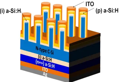
Figure 1-1: Global and regional cumulative capacity in Megawatt (MW) [4]. ... 36 Figure 1-2: TOP 10 countries in 2014 for cumulative installed capacity [4]. ... 37 Figure 1-3: TOP 10 countries in 2014 for annual installed capacity [4]. ... 38 Figure 1-4: Timeline of the best research cell efficiencies for the different PV technologies [19]. ... 41 Figure 1-5: Illustration of the light trapping effect of SiNWs. This light trapping effect by SiNWs is directly visible with the eye as shown by the back color of SiNWs sample compared to the shiny grey aspect of the planar reference sample. It shows that the light is effectively trapped within the SiNWs. ... 43 Figure 2-1: (a) Diffusion current at the interface between the p-type and n-type semiconductor in order to equalize the concentration of holes (white circle) and electrons (black circles). The green positive sign symbolize the phosphorus cations and the red negative sign symbolizes the boron anion which are doping the semiconductors.(b) Formation of the space charge region, depleted in charge carriers. The phosphorus and boron dopants create an internal electric field at the p-n junction. ... 53 Figure 2-2: Equivalent circuit model of a solar cell [39]. ... 55 Figure 2-3: (I,V) curve of a solar cell and definition of the photovoltaic parameters [40]. ... 56 Figure 2-4: Scheme of the VLS Vapor Liquid Solid process [54]. ... 58 Figure 2-5: Mechanism of formation of SiNW by the MACE process. A silicon substrate is dipped in HF/AgNO3 solution [61], [62] ... 60 Figure 2-6: SEM picture of 10 µm SiNWs fabricated by MACE showing the strong agglomeration at the top-end of the SiNWs ... 61 Figure 2-7: Reflectance measurement of porous (PSi), polished c-Si and SiNW arrays [26], [27]. ... 62 Figure 2-8: Advantages and drawbacks of the radial, axial and substrate junctions [68] ... 68 Figure 2-9: Schematic representation of the atomic structure of crystalline silicon (a) and hydrogenated amorphous silicon (b). For c-Si, every Si atom is linked to four other Si atoms and the overall structure is long range ordered. For amorphous silicon, only a short range order is visible because of variation in the angle and length of covalent bonds. Many coordination defects which are not passivated by hydrogen are present within the structure [121]. ... 82 Figure 2-10: Schematic representation of the band diagram of crystalline silicon (a) and hydrogenated amorphous silicon (b). In a perfect crystal, the band gap is well defined and Eg = Ev-Ec. Blue color represents sates with delocalized wavefunctions. For a-Si:H states are present within the band gap. Orange and purple colors represent the localized wavefunctions, responsible for the reduced mobility properties of a-Si:H. Defects states are due to the dangling bonds defects and tail states are induced by bonding distortion [121]. ... 83 Figure 2-11: Schematics of a standard HIT heterojunction solar cell [125]. ... 85
TOGONAL Aliénor Svietlana | PhD Thesis | Nanyang Technological University and Ecole Polytechnique | 2015 24
Figure 2-12: Schematics of the band diagram of a HIT for a n-type c-Si [126]. ... 86 Figure 2-13: Schematic of a HIT structure based on SiNWs. The n-type c-Si wafer has been nanostructured to improve light trapping ... 88 Figure 2-14: Schematic representation of an ideal nanostructure hybrid silicon/organic material solar cell. The nanowires offer a continuous conductive path to the electrode. Lexc is the
diffusion length of the exciton. The nanowires are separated by a distance of about 2Lexc, in
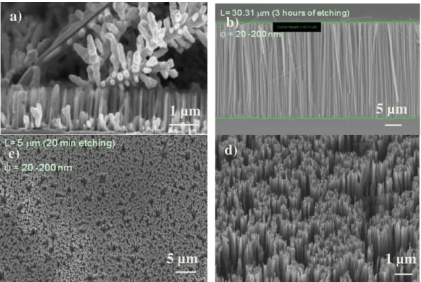
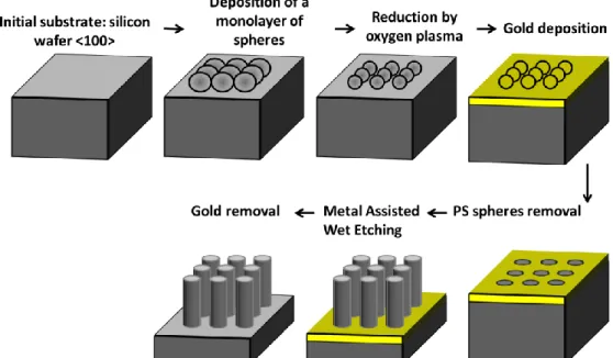
order to reduce loss in photocurrent due to exciton recombination. ... 90 Figure 3-1: Schematics of the nanosphere lithography method coupled with the MACE process ... 94 Figure 3-2: (a) SEM picture of silver dentrites covering the SiNW prior the HNO3 chemical bath [142], (b) cross-section SEM picture of 30 µm long random SiNWs, (c) inclined (15°) SEM picture of 5 µm long random SiNWs, and (d) inclined (30°) SEM picture of 5 µm long SiNWs. ... 95 Figure 3-3: Schematics of the nanosphere lithography method coupled with the MACE process ... 96 Figure 3-4: Schematics of the floating-transferring technique to achieve an hexagonal compact arrangement of PS spheres on a silicon substrate [143]... 97 Figure 3-5: (a) Schematics of the flotation capillary forces, the driving force for the self-assembly of the PS spheres [147]. (b) Photograph of the monolayer obtained onto the water surface. ... 98 Figure 3-6: Photograph of the "transfer" stage where the silicon substrate is placed below the PS monolayer and dragged upward to coat the sample by the PS suspension. ... 99 Figure 3-7: (a) Photograph of the Si substrate covered by a monolayer of PS spheres. (b) Low-magnification SEM image of perfectly ordered PS spheres arranged into an hexagonal compact arrangement. (c) ) High-magnification SEM pictures of perfectly ordered PS spheres arranged into an hexagonal compact arrangement. (d) SEM picture of the PS film showing that the film is not uniform everywhere. Small domains coexist with different orientations. ... 100 Figure 3-8: Schematics illustrating the effect of the plasma etching treatment on the PS spheres. ... 101 Figure 3-9:SEM picture of (a) slightly annealed PS spheres. The red circles shows the small area melted. (b) Overheated PS spheres causing the excessive melting of the colloidal particles. ... 101 Figure 3-10: The etch rate of the PS spheres with initial nominal diameter of 500 nm, 600 nm and 800 nm by oxygen plasma as a function of time. ... 102 Figure 3-11: SEM picture of the PS spheres arrays after 130s of oxygen plasma treatment. The PS spheres are separated from each other. The initial diameter of PS spheres of 600 nm was reduced down to 392 nm. ... 103 Figure 3-12: SEM pictures of PS sphere arrays covered by a 25 nm gold thin film. ... 103 Figure 3-13: (a) SEM pictures of the gold etching mask after the removal of the PS spheres. (b) SEM pictures of SiNWs arrays where the removal stage of PS spheres has been carried out at
the last step of the process. The PS spheres are not effectively removed since they are trapped inside the nanostructure. ... 104 Figure 3-14: (a) SEM pictures of (a) high density SiNWs ordered arrays (inclined 30°) samples with 800 nm pitch , (b) low density SiNWs ordered arrays (inclined 30°) with 800 nm pitch, (c) cross section of short SiNWs, and (d) cross section of long SiNWs. ... 105 Figure 3-15: Schematics illustrating the voltage distribution of a plasma in the case of asymmetric electrodes [148]. ... 108 Figure 3-16: The Paschen curve showing the breakdown voltage as a function of the product of the pressure p with the interdistance between the electrodes d [152]. ... 111 Figure 3-17: Photographs of the (a) ARCAM chamber and (b) ARCAM control panel ... 112 Figure 3-18: (a) Schematics [154] and (b) corresponding photograph of the e-beam evaporator. ... 113 Figure 3-19: (a) Schematics [155] and (b) photograph of the sputtering system. (c) O2:Ar plasma during the ITO deposition. ... 114 Figure 3-20: Schematics illustrating the key steps of the spin coating technique [156]. ... 114 Figure 3-21: The ideal and typical EQE response of a silicon solar cell from www.pveducation.org. ... 116 Figure 3-22: Schematics of TRMC experimental set up [169]. ... 119 Figure 3-23: (a) Schematics of the EBIC set up [178] and (b) photograph of the EBIC equipment. ... 121 Figure 3-24: Schematics and photograph of the UV/Vis/NIR spectrophotometer (PerkinElmer) using an integrating sphere. ... 122 Figure 3-25: Schematics illustrating the working principle of Mueller matrix ellipsometer .... 123 Figure 3-26: Schematics showing the working principle of the Angle-resolved MM polarimeter [179]. ... 124 Figure 4-1: Schematic representation of two cylinders of the same length L and radii R, separated by a distance d and partially immersed in a liquid. Once the water level falls below the tip of the cylinders during the drying process, the surface tension of the liquid/vapor interface γLV induces a small curvature of the solvent to reduce the active surface area ... 128
Figure 4-2: Schematic illustration of the forces acting on two SiNWs partially immersed in a liquid. The bending of the SiNWs stems from a balance between the Van der Waals (FVdW) and
the surface tension (FST) attractive forces and the repulsive elastic deformation force FED. γLV is
the surface tension which characterizes the liquid/vapor interface. is the deflection of the NW. ... 131 Figure 4-3: Schematic model of an array composed of three 2 µm long-nanowires labeled 1, 2 and 3. Definition of the original geometry- the ideal case (a). Definition of the forces: FX/Y is the
force exerted by SiNW #X on SiNW #Y (b). Definition of the equilibrium position before (nanowire in dotted lines) and after bending (c). ... 133 Figure 4-4: Equilibrium position of SiNW #2 as function of its initial position. When the interspacing Δ between two nanowires in the array is short, any minor irregularity ( X/Δ > 0.2
TOGONAL Aliénor Svietlana | PhD Thesis | Nanyang Technological University and Ecole Polytechnique | 2015 26
or X/Δ < -0.2)) lead to adhesion of the nanowires (Xeq/Δ = 1/-1) whereas for larger nanowires-interspacing Δ, adhesion occurs for larger irregularities (X/Δ > 0.6 or X/Δ < -0.6). ... 134 Figure 4-5: Effect of the length on the Van der Waals, capillary and elastic deformation forces ... 135 Figure 4-6: (a) Schematic detailing the fabrication process of agglomerated and tapered SiNWs. (b) Schematic showing the effect of KOH post-etching treatment to taper the top-ends of SiNWs [186], [193] ... 138 Figure 4-7: (a) Cross-section SEM images of the SiNW array after MACE with a scale bar of 10 μm. Inclined (30°) SEM images showing the effect of KOH post-etching treatment on the morphology of SiNWs as a function of the etching time: (b) 0 s, (c) 30 s, (d) 60 s,(e) 120 s, and (f) 240 s. Scale bars in (b)−(f) are 5 μm [186], [193]. ... 139 Figure 4-8: Schematic illustrating the principle of strengthen mechanically the nanowires by a polymer. ... 141 Figure 4-9: SEM pictures of SiNWs arrays (a) before and (b) after the replacement of solvent. ... 143 Figure 4-10: Effect of KOH post-treatment on the morphology of SiNWs for different time of treatment and for different magnification. ... 145 Figure 4-11: Effect of power on the etching of SiNWs (a) At 100 Watt, the SiNWs collapse and lied on the wafer. (b) At 200 Watt, the SiNWs are completely etched away. ... 147 Figure 4-12: SEM pictures of SiNWs arrays (a) before and (b) after RIE post-treatment. ... 148 Figure 4-13:SiNWs array (a) before and (b) after CO2 supercritical drying process. ... 149 Figure 4-14: Top view (a), (b) and cross-section (c), (d) SEM pictures: Effect on the morphology of the SiNWs fabricated by MACE with a HF pre-treatment (a), (c) and with a H2O2:H2SO4 pre-treatment (b), (d). The insets show high magnification SEM images of the top-view. The scale bar is 500 nm. ... 152 Figure 4-15: Reflectance of the SiNW arrays fabricated by MACE with a HF pre-treatment (solid black squares), a H2O2:H2SO4 pre-treatment (black solid circles) a HF pre-treatment and a HF post-treatment (open squares), and after a H2O2:H2SO4 pre-treatment and HF post treatment (open circles). ... 153 Figure 4-16: SEM pictures - Effect on the morphology of the SiNWs fabricated by MACE after a H2O2:H2SO4 pre-treatment (a), after a H2O2:H2SO4 pre-treatment and a HF post-treatment (b), after a HF pre-treatment (c), (e), and after a HF pre-treatment and a HF post-treatment (d), (f). The insets show high magnification SEM images of the top-view. The scale bar is 500 nm. .. 154 Figure 4-17: Measurement of contact angle on SiNWs after the standard MACE process (after HNO3 bath) (left) and after HF post-treatment (right). ... 155 Figure 4-18: Schematic illustration of the water meniscus shape according to the wettability of SiNWs. For hydrophilic SiNWs, the water is wetting on the surface and the meniscus is concave (a) while for hydrophobic SiNWs, the water is non-wetting and the meniscus is convex (b). ... 157
Figure 4-19: Cross-section SEM pictures of 30 µm long nanowires: Effect on the morphology of the SiNWs fabricated by MACE with no post-treatment (a) and after a HF post-treatment (b). The insets show SEM images of the top-view. The scale bar is 5 µm. ... 157 Figure 5-1: Reproducibility of the measured total reflectance data for 2 different samples. Measurements were performed at different locations of the sample on different days, showing good sample uniformity and measurement reproducibility. ... 160 igure 5-2 omparison of the total reflectance bet een commercial p ramids (blac curve) and ordered Si s arra s of 165 nm height and pitch of 330 nm (red curve) and disordered SiNWs with a length of 500 nm (green curve) with the corresponding SEM pictures ... 161 Figure 5-3: Effect of disordered SiNW length on the measured total reflectance plotted as a function of the wavelength. ... 161 Figure 5-4: Spectral dependence of the total reflectance measured on ordered SiNWs with pitch of 330 nm, diameter of 250 nm (+/- 10 nm) and lengths of 165 nm, 2 µm, 4 µm and 8 µm. ... 162 Figure 5-5: Cross-section SEM images of ordered SiNW arrays with a pitch of 330 nm, an average diameters between 239-259 nm and lengths of (a) 163 nm, (b) 2.1 µm, (c) 4.2 µm and (d) 8.2 µm, respectively. The inset in (d) shows the corresponding top-view SEM image. ... 163 Figure 5-6: Figure 5-7: Illustration of SEM image analysis by imageJ: (a) original image, (b) threshold image, (c) image contour analysis and (d) area distribution. ... 164 Figure 5-8: Effect of the volume fraction on the reflectance of three ordered arrays of SiNWs with a pitch of 600 nm and a length of 2 µm. The diameters for the high, medium and low density SiNW arrays are 503 nm, 436 nm and 158 nm. ... 165 Figure 5-9: Schematic of the working principle of an anti-reflective coating [221]. ... 166 Figure 5-10: Effect of increasing the thickness of ITO on the reflectance of ordered SiNW arrays with a pitch of (a) 250 nm and (b) 500 nm. ... 166 Figure 5-11: Top-view SEM image of ordered arrays of SiNWs with a pitch of 250 nm covered with a thickness of ITO of (a)75 nm and (b) 100 nm. ... 169 Figure 5-12: Illustration of a diffraction pattern from a periodic diffraction grating [222] ... 170 Figure 5-13: Circular diffraction pattern on NWs ... 171 Figure 5-14: (a) Real space (microscopic) image and (b) corresponding measured normalized Mueller matrices of ordered SiNW arrays with a pitch of 800 nm. ... 173 Figure 5-15: (a), (c), (e) Real space (microscopic) image and (b), (d), (f) corresponding M11 element detail of the measured Mueller matrices for a single domain (a), (b) , exactly 2 different domains (c), (d) and many small domains (e), (f)... 175 Figure 5-16: Definition of the 3 different layers used in our RCWA modeling. ... 176 Figure 5-17: Effect of the geometrical parameters (pitch and length) on the estimated Jsc for a perfect periodic structure. ... 177 Figure 5-18: Structural imperfections of ordered array of SiNWs fabricated by MACE assisted by NSL such as (a) surface roughness, (b) dislocations, (c) diameter distribution and (d) domain orientations. ... 178
TOGONAL Aliénor Svietlana | PhD Thesis | Nanyang Technological University and Ecole Polytechnique | 2015 28
Figure 5-19: (a) Cross-section and (b) top-view SEM image of short ordered arrays of SiNWs and corresponding modeling (c) , (d) using the "periodic model". ... 180 Figure 5-20: Comparison between (a) the "periodic model and (b) the "statistical model" for modeling a short periodic array fabricated by MACE assisted by NSL. ... 180 Figure 5-21: Best fit of Mueller Matrix using the statistical model. ... 182 Figure 5-22: Representation of the dual diameter SiNW arrays concept with the corresponding Poynting vector at a wavelength of 450 nm. Every black circle represent a nanowire [37], [38]. ... 183 Figure 5-23: Top-view SEM pictures of PS spheres monolayer with a PS sphere (330:600 nm) ratio of (a) (1:2), (b) (2:1) and (c) corresponding SiNW arrays fabricated from (b). ... 184 Figure 5-24: Reflectance spectra of dual diameter SiNW array with (330 nm : 600 nm) (2:1). ... 185 Figure 6-1: Schematic of the structure of (a) a HIT solar cells [125] (b) a HIT solar cell where the n-type c-Si wafer has been nanostructured to improve light trapping. ... 187 Figure 6-2: Illustration of a hexagonal SiNWs arrays with a pitch p and a height h (left) and calculation of the surface ratios for different geometries (right). ... 189 Figure 6-3: (a) Schematic of the structure of the HIT solar cell where the n-type c-Si wafer has been nanostructured to improve light trapping. (b) SEM cross-section of a fabricated device. 190 Figure 6-4: Process of fabrication of HIT solar cells based on SiNWs. ... 191 Figure 6-5: Dependence of (a) EQE and (b) (J,V) curves on the thickness of the amorphous layer (see Table 6-1). ... 192 Figure 6-6: The average value and the standard deviation of Jsc (a), FF (b), Voc (c) and η (d) as
function of da-Si:H. ... 194 Figure 6-7: SEM pictures of SiNW solar cells after a-Si:H PECVD deposition of sample D (a) and sample F (b) before ITO deposition and sample F (c) after ITO deposition cross-section and (d) after ITO deposition top-view. ... 195 Figure 6-8: TRMC signal as a function of time for HIT solar cells with different a-Si:H thicknesses. The inset shows the signal in logarithmic scale. ... 197 Figure 6-9: Schematic showing the details of the a-Si:H coating. ... 198 Figure 6-10: Effect of the gradient doping on (J,V) curves of HIT solar cells based on SiNWs. ... 200 Figure 6-11: Effect of the gradient doping on the EQE of HIT solar cells based on SiNWs. .. 201 Figure 6-12: Effect of the (i) a-Si:H thickness on the EQE of HIT solar cells based on SiNWs. ... 203 Figure 6-13: Effects of the SiNWs length on the (a) EQE and (b) reflectance of the cells. ... 205 Figure 6-14: TRMC signal as a function of time for samples with different SiNW lengths. ... 206 Figure 6-15: TEM analysis of disordered SiNWs. SiNWs agglomerate (a) and (b). Only the tip of the wire is covered by a-Si:H and the coating depth by a-Si:H is between 370- 500 nm (c), (d) and (e). Small crystal grains can be found within the amorphous coating (f) and (g). ... 209
Figure 6-16: : EBIC mapping of the HIT SiNW cross-section under various accelerating voltages (a) 3 keV, (b) 5 keV and (c) 10 keV. ... 210 Figure 6-17: EBIC current profile at 10 keV as a function of position of the beam on the sample C with the corresponding EBIC mapping in the inset. The red arrow in the inset indicates the corresponding signal position on the sample. A cross-section schematic of the structure is displayed at the bottom. ... 211 Figure 6-18: Equation (4) as a function of x, the distance from the junction, obtained from experimental data of zone 2 in Figure 6-17. ... 212 Figure 6-19: (a) Cross-section SEM image of the bottom of a SiNW partially covered by ITO and (b) corresponding EBIC mapping with the red arrow indicating the corresponding signal position on the sample and (c) the corresponding EBIC current profile at 10 keV as a function of the position of the beam on the sample. (d) Cross-section EBIC mapping of samples with “dead” and electricall active Si s. The inset sho s the EBI top-view mapping confirming that only few nanowires are active. ... 213 Figure 6-20: Modeling of the volume of excitation produced by a 10 keV electron beam impinging on a 550 µm c-Si substrate with (a) no ITO, (b) 100 nm of ITO and (c) 200 nm of ITO. ... 214 Figure 6-21: EBIC current profiles (a) and cross-section EBIC current mapping (b). The 4 different arrows indicate the localization of the different EBIC profiles measured on the sample. ... 214 Figure 6-22: EBIC mapping of SiNW solar cells based on 5 m epitaxial film with low magnification in (a) grey and (b) rainbow magnification and (c) high magnification . ... 216 Figure 6-23: EQE (a) and (I,V) (b) curves of reference planar cell and SiNWs based solar cells on 5 m Si epitaxial thin film. ... 217 Figure 6-24: SEM picture of ordered arrays of SiNWs (pitch 550 nm, diameter of 345 nm , length of 1.2 µm) after a-Si:H depositon and before ITO deposition (a) top-view (b) cross-section ... 218 Figure 6-25: Top-view SEM image of ordered arrays of SiNWs covered with a thickness of ITO of (a) 25 nm, (b) 50 nm, (c) 75 nm and (d) 100 nm. (e) shows the cross-section of a single SiNW with various thicknesses of ITO. ... 219 Figure 6-26: Comparison of EQE response for different C-Si substrates: reference planar cells, ordered SiNW arrays cells, disordered SiNW arrays cells. ... 221 Figure 6-27: Comparison of EQE response for different epitaxial c-Si substrates: reference planar cells, ordered SiNW arrays cells, disordered SiNW arrays cells. ... 221 Figure 6-28: Cross-section SEM picture of ordered arrays of SiNWs (pitch 330 nm, diameter 220 nm, length 700 nm) (a) at low and (b) high magnification. The inset (b) shows that the top of the wire is less damaged for short SiNWs (250 nm height). ... 222 Figure 6-29: EELS analysis of ordered SiNW arrays. ... 223 Figure 6-30: TEM analysis of ordered SiNW before a-Si:H coating... 225
TOGONAL Aliénor Svietlana | PhD Thesis | Nanyang Technological University and Ecole Polytechnique | 2015 30
Figure 6-31: TEM analysis of ordered SiNW after Si:H coating.The coating of SiNWs by a-Si:H is not uniform (a), (b), it is maximum at the tip of the SiNW (c) and present a columnar structure (c) and (d). Finally, some crystalline grains are observed at the bottom of the coating (e)... 227 Figure 6-32: Top-view EBIC mapping of ordered SiNWs arrays (pitch of 500 nm, diameter of 280 nm and height of 460 nm) at different gun energies: 3 keV (a), 10 keV (b) and 20 keV (c) with the corresponding modeling (d), (e) and (f ). ... 228 Figure 6-33: Cross-section EBIC mapping of short (a), (b) and long (c), (d) ordered SiNWs arrays at 2 different gun energies: 5 keV (a), (c) and 10 keV (b), (d) ... 229 Figure 6-34: Top-view EBIC mapping of ordered SiNWs arrays with a length of (a) 500 nm, (b) 2.2 µm and (c) 3 µm. ... 230 Figure 6-35: (a) Top-view SEM image of the silver etching mask after the removal of the PS spheres. (b) Top view SEM image after 20 s wet chemical etching and removal of silver film (c) ) Top view SEM image after 45 s wet chemical etching and removal of silver film (d) Cross-section SEM picture of SiNWs fabricated by MACE assisted by NSL with silver catalyst after 1 min etching. ... 231 Figure 6-36: Illustration of the oxidation process ... 232 Figure 6-37: Top-view SEM picture of ordered arrays of SiNWs (pitch 800 nm, length of 2.7 µm) before (a) and after (b) oxidation process. ... 232 Figure 6-38: Effect of oxidation treatment on EQE ... 234 Figure 6-39: Top-view EBIC mapping before (a) and after (b) oxidation pre-treatment. ... 234 Figure 6-40: Cross-section SEM pictures (a) and corresponding EBIC mapping (b) of samples which underwent an oxidation pre-treatment ... 235 Figure 7-1: Schematic detailing the architecture of the hybrid device ... 237 Figure 7-2: Process flow of hybrid solar cells ... 239 Figure 7-3: EQE response of the three arrays of ordered SiNW arrays A, B and C and (b) the corresponding average reflectance on the spectrum range 350-1100 nm. ... 241 Figure 7-4: (a) (J,V) and (b) EQE of hybrid devices based on disordered and ordered SiNWs. ... 242 Figure 7-5: Band diagram of the hybrid device ... 243 Figure 7-6: Cross-section view (a), (b), Top-view (c) and Inclined-view (d) SEM pictures of SiNWs coated with PEDOT:PSS... 244 Figure 7-7: SEM pictures of ordered SiNWs after (a) LPAD1, (b) LPAD2 and (c) LPAD3. .. 246 Figure 7-8: (a) Cross section view of a-Si:H nanowires. (b) Top-view of a-Si:H nanowires. (c) Length of nanowires as a function of the etching time. ... 249 Figure 7-9: Reflectance measurement of planar a-Si:H thin films and a-Si:H nanowires. ... 250 Figure 7-10: Top-view (a) and inclined 30° (b) SEM pictures of a-Si:H NWs. ... 250 Figure 7-11: Architecture of the device studied – Hybrid thin film solar cells based on a-Si:H. ... 252 Figure 7-12: (a) (J,V) and (b) EQE planar hybrid a-Si:H / PEDOT:PSS heterojunction ... 253
Figure 7-13: Schematic of the hybrid solar cells based on the combination of an organic layer with an amorphous thin film with a LiF/Al rear electrodes. ... 254 Figure 7-14: Effect of C60 thickness on the performance of the solar cells. ... 255 Figure 7-15: Schematic of the vacuum level shift induced by LiF/Al cathode for organic solar cells. ... 257 Figure 7-16: Schematic of the structure of the LiF/Al rear electrodes on (p+) a-SiC:H/(i) a-Si:H. ... 258 Figure 7-17: (J,V) curves of the thin film devices with LiF/Al cathode (black) and Al cathode (red). ... 259 Figure 7-18: EQE curves of the thin film devices with LiF/Al cathode (black) and Al cathode (red) ... 261 Figure 7-19: Schematic of the band diagram of p-i-n junction and a-Si:H thin film with a LiF/Al rear electrodes. ... 263 Figure 7-20: (J,V) curves of the thin film devices with LiF/Al cathode (black) and Al cathode (red). ... 263 Figure 7-21 Light soa ing effect on the cells’ performances. ... 265 Figure 7-22 Effect of the electrode size on the solar cells’ parameters ... 266
List of Tables
Table 2-1: Key results and finding on SiNWs based Solar Cells. ... 72 Table 4-1: Main advantages and drawbacks of the different methods used to separate agglomerated SiNWs. ... 158 Table 5-1: Average reflectance over the spectral range 400-1100 nm for disordered SiNWs with different lengths ... 162 Table 5-2: Geometrical parameters of 4 different ordered SiNW arrays with the corresponding average total reflectance calculated in the range of 400-1100 nm. ... 163 Table 5-3: Effect of ITO coating on the average reflectance of ordered arrays of SiNWs. Jsc is
calculated from the absorbed photons and Jloss is calculated from the reflected photons... 169
Table 6-1: Summary of various deposition conditions with details of the deposition time of each layer. ... 192 Table 6-2: The average value and the standard deviation of Voc, Jsc, FF and η of core-shell HIT
solar cells. ... 193 Table 6-3: Summary of various deposition conditions with details of the deposition time of every layer and average value of Voc, Jsc, FF and η of corresponding core-shell HIT solar cells.
... 198 Table 6-4: Summary of various deposition conditions with details of the deposition time of every layer and average value of Voc, Jsc, FF and η of corresponding core-shell HIT solar cells.
... 201 Table 6-5: Dependence of the photovoltaic parameters Jsc, FF, Voc and η on the length of
SiNWs. ... 204 Table 6-6: Photovoltaic parameters for reference planar cells and SiNWs based solar cells on 5
m epitaxial layer. ... 216 Table 6-7: Summary of geometrical characteristics of SiNW arrays and average value of Voc,
Jsc, FF and η of corresponding core-shell heterojunction solar cells. ... 220
Table 6-8: Effect of oxidation treatment: summary of geometrical characteristics of SiNW arrays and average value of Voc, Jsc, FF and η of corresponding core-shell heterojunction solar
cells. ... 233 Table 7-1: Summary of the geometry of the different SiNW arrays and average value of Voc, Jsc,
FF and η of corresponding hybrid solar cells. ... 240
Table 7-2: Average value of Voc, Jsc, FF and η of planar hybrid a-Si:H / PEDOT:PSS
heterojunction ... 253 Table 7-3: Effect of the thickness of C60 on the average value of Voc, Jsc, FF and η of planar
hybrid a-Si:H / C60 heterojunction ... 254 Table 7-4: Comparison of photovoltaic parameters of thin film devices with Al cathode and LiF/Al cathode. ... 260 Table 7-5: Photovoltaic Performance - Effect of LiF thickness. ... 264 Table 7-6: Effect of LiF thickness on the series resistances. ... 264
TOGONAL Aliénor Svietlana | PhD Thesis | Nanyang Technological University and Ecole Polytechnique | 2015 34
Chapter 1 : Introduction
"The ultimate answer to humanity’s energy problems rises every morning and sets every evening."
Oliver Morton Editorial, Nature, 14th August 2008
1.1 Solar energy: the Reality and the Future of Photovoltaics
Energy is undoubtedly the challenge of the century, if not the millennium, because of its potential economic, political and environmental fallouts. Nowadays fossil fuels account for around 80% [1] of the global energy consumption. The orld’s heav dependence, especiall on oil, is particularly worrying because of the inevitable decline of its supply, and the resulting pollution of water and air by greenhouse gas emissions [2]. As fossil fuel resources are becoming scarce and even more challenging to explore, it is unlikely that the oil industry will be able to keep up with the path of an ever increasing global energy demand, driven by both population and economic growth. Therefore, in response to increasing stress on fossil fuel resources, new concepts such as green energy or sustainable living have emerged, leading to the development of alternative energy sources such as wind energy, solar energy, geothermal energy, tidal energy, biomass, wave power, biodiesel, hydrogen fuel, etc. Among them, solar energy power, as a clean and inexhaustible energy source, is believed to be one of the most promising candidates to help solve the problems of energy shortage and environmental problems
Indeed solar energy has very attractive features. It is a free, clean and infinite energy source which, once installed, produces no pollution, no emission, no carbon footprint and no noise. Solar energy has also the potential
TOGONAL Aliénor Svietlana | PhD Thesis | Nanyang Technological University and Ecole Polytechnique | 2015 36
to cover the global energy demand: every hour, the earth receives more energy
from the sun than mankind can consume in a year [3]. Harvesting a small
fraction of this energy could solve the problem of energy shortage, hence many efforts have been put into the research and development of efficient solar cells.
While solar PV was only a niche market one decade ago with small scale applications (calculator, watch, out of grid…), it is no ada s a mature technology and industry on its way to become a mainstream source of electricity. Over the last two decades, the global cumulative installed capacity has grown exponentially from around 5 gigawatt (GW) in 2005 to 177 GW by the end of the year 2014 as shown in Figure 1-1 [4]. For the year 2014 alone, 38.7 GW were newly installed worldwide, led by China (10.0 GW), Japan (9.7 GW) and USA (6.2 GW). Italy, Greece and Germany are now able to cover respectively 7.9%, 7.6% and 7.0% of their annual energy demand by solar energy [4]. Therefore PV is no longer a chimera, but instead can contribute significantly to a sustainable energetic transition.
Figure 1-1: Global and regional cumulative capacity in Megawatt (MW) [4].
Japan and Europe have driven for a long time the growth of photovoltaics. In particular, Germany still holds the world record of the highest cumulative solar PV capacity installed in 2014 (38.23 GW) as shown in Figure
1-2 [4]. However, the competition is fierce and China is expected to take the
lead by 2017 with a predicted PV capacity of 70 GW. The European PV market has slowed down over the past 4 years with a significant drop from 22 GW in
Europe Asia
Middle East & Africa Asia
China
2011 to 7 GW in 2014. This is explained by a context of reduced feed-in tariffs, retroactive measures and declining political support which have contributed in the past to the development of the European PV market. European, Japanese and US manufacturers have also suffered from the competition of Chinese and Taiwanese manufacturers which have become today the main module suppliers.
Figure 1-2: TOP 10 countries in 2014 for cumulative installed capacity [4].
Today, the PV market is dominated by Asia which constitutes about 60% of the global PV market. The PV growth is also boosted by emerging markets such as South Africa, Chile, Mexico and Turkey while the European market continues its decline despite the significant growth of the UK installed capacity in 2014 (2.27 GW). Figure 1-3 shows the added installed capacity country by country for the year 2014 [4]. China and Japan are far beyond the other countries. In 2014, Japan underwent a real boom (9.2 GW) while the Chinese market tends to stabilize (10.6 GW). The landscape of the PV market is therefore changing quickly with new actors entering the play.
25% 19% 16% 12% 12% 4% 4% 3% 3% 2%
Germany China Japan Italy USA France Spain UK Australia Belgium
TOGONAL Aliénor Svietlana | PhD Thesis | Nanyang Technological University and Ecole Polytechnique | 2015 38
Figure 1-3: TOP 10 countries in 2014 for annual installed capacity [4].
Forecasting the evolution of the PV market is always a delicate and complex issue. Official agencies such as IEA (International Energy Agency) are predicting solar deployment every year but frequently they have to adjust their numbers. For the year 2015, the expected solar growth should be between 35 GW to 57.3 GW, according to the different scenarios established by different agencies or companies [5]–[7]. The market share of crystalline silicon is predicted to increase at the detriment of polycrystalline silicon [8].
Despite the considerable advantages offered by solar energy, cumulative photovoltaic (PV) electricity production represents today only 1% of the total global electricity production [4]. Therefore a legitimate question arises: what are the limitations towards a global PV deployment?
The major limitation, when the subject comes up, remains the initial cost, although it is becoming less and less true. Solar panels and other units for collection and storage are relatively expensive to manufacture, making solar energy a costly option for generating electricity. The time lag of several years for matching initial investment is still prohibitive for many customers. This high cost can be partly explained by the expensive silicon wafer technology which has been widely used as the base component for achieving stable and efficient solar cell devices because of its unique properties. Indeed solar cells based on crystalline silicon (c-Si) wafers have dominated the photovoltaic market since the very beginning of the PV industry, bac in the 1950’s, maintaining since then a market share of about 80% [9]. In 2014, Panasonic
30% 28% 18% 7% 5% 2% 3% 3% 2% 2%
China Japan USA UK Germany
![Figure 1-4: Timeline of the best research cell efficiencies for the different PV technologies [19]](https://thumb-eu.123doks.com/thumbv2/123doknet/2897083.74358/42.892.160.739.113.449/figure-timeline-best-research-cell-efficiencies-different-technologies.webp)
![Figure 2-5: Mechanism of formation of SiNW by the MACE process. A silicon substrate is dipped in HF/AgNO 3 solution [61], [62]](https://thumb-eu.123doks.com/thumbv2/123doknet/2897083.74358/61.892.318.697.112.488/figure-mechanism-formation-process-silicon-substrate-dipped-solution.webp)
![Figure 2-12: Schematics of the band diagram of a HIT for a n-type c-Si [126].](https://thumb-eu.123doks.com/thumbv2/123doknet/2897083.74358/87.892.164.731.451.736/figure-schematics-band-diagram-hit-n-type-si.webp)
![Figure 3-4: Schematics of the floating-transferring technique to achieve an hexagonal compact arrangement of PS spheres on a silicon substrate [143]](https://thumb-eu.123doks.com/thumbv2/123doknet/2897083.74358/98.892.187.639.262.533/figure-schematics-floating-transferring-technique-hexagonal-arrangement-substrate.webp)
![Figure 3-5: (a) Schematics of the flotation capillary forces, the driving force for the self-assembly of the PS spheres [147]](https://thumb-eu.123doks.com/thumbv2/123doknet/2897083.74358/99.892.163.746.693.916/figure-schematics-flotation-capillary-forces-driving-assembly-spheres.webp)

![Figure 3-20: Schematics illustrating the key steps of the spin coating technique [156]](https://thumb-eu.123doks.com/thumbv2/123doknet/2897083.74358/115.892.268.629.748.1018/figure-schematics-illustrating-key-steps-spin-coating-technique.webp)
